


128 Mbit (8Mb x 16, Multiple Bank, Burst)
FEATURES SUMMARY
■ SUPPLY VOLTAGE
= 1.65V to 2.2V for Program, Erase and
–V
DD
Read
–V
–V
■ SYNCHRONOUS / ASYNCHRONOUS READ
– Synchronous Burst Read mode: 54MHz
– Asynchronous/ Synchronous Page Read
– Random Access: 70, 80, 100ns
■ SYNCHRONOUS BURST READ SUSPEND
■ PROGRAMMING TIME
– 8µs by Word typical for Fast Factory Program
– Double/Quadruple Word Program option
– Enhanced Factory Program options
■ MEMORY BLOCKS
– Multiple Bank Memory Array: 4 Mbit Banks
– Parameter Blocks (Top or Bott o m location)
■ DUAL OPERATIONS
– Program Erase in one Bank while Read in
– No delay between Read and Write operations
■ BLOCK LOCKING
– All blocks locked at Power up
– Any combination of blocks can be locked
–WP
■ SECURITY
– 128 bit user programmable OTP cells
– 64 bit unique device number
– One parameter block permanently lockable
■ COMMON FLASH INTERFACE (CFI)
■ 100,000 PROGRAM/ERASE CYCLES per
BLOCK
= 1.65V to 3.3V for I/O Buffers
DDQ
= 12V for fast Program (optional)
PP
mode
others
for Block Lock-Down
M58WR128ET
M58WR128EB
1.8V Supply Flash Memory
PRODUCT PREVIEW
Figure 1. Package
FBGA
VFBGA60 (ZB)
12.5 x 12mm
■ ELECTRONIC SIGNATURE
– Manufacturer Code: 20h
– Top Device Code, M58WR128ET: 881Eh
– Bottom Device Code, M58WR128EB: 881Fh
May 2003
This is preliminary information on a new product now in development. Details are subject to change without notice.
1/87

M58WR128ET, M58WR128EB
TABLE OF CONTENTS
SUMMARY DESCRIPTION. . . . . . . . . . . . . . . . . . . . . . . . . . . . . . . . . . . . . . . . . . . . . . . . . . . . . . . . . . . 7
Figure 2. Logic Diagram . . . . . . . . . . . . . . . . . . . . . . . . . . . . . . . . . . . . . . . . . . . . . . . . . . . . . . . . . . 8
Table 1. Signal Names . . . . . . . . . . . . . . . . . . . . . . . . . . . . . . . . . . . . . . . . . . . . . . . . . . . . . . . . . . . 8
Table 2. Bank Architecture . . . . . . . . . . . . . . . . . . . . . . . . . . . . . . . . . . . . . . . . . . . . . . . . . . . . . . . . 9
Figure 3. VFBGA Connections (Top view through package) . . . . . . . . . . . . . . . . . . . . . . . . . . . . . . . 9
Figure 4. Memory Map . . . . . . . . . . . . . . . . . . . . . . . . . . . . . . . . . . . . . . . . . . . . . . . . . . . . . . . . . . 10
SIGNAL DESCRIPTIONS . . . . . . . . . . . . . . . . . . . . . . . . . . . . . . . . . . . . . . . . . . . . . . . . . . . . . . . . . . . 11
Address Inputs (A0-A22). . . . . . . . . . . . . . . . . . . . . . . . . . . . . . . . . . . . . . . . . . . . . . . . . . . . . . . . . 11
Data Input/Output (DQ0-DQ15). . . . . . . . . . . . . . . . . . . . . . . . . . . . . . . . . . . . . . . . . . . . . . . . . . . . 11
Chip Enable (E). . . . . . . . . . . . . . . . . . . . . . . . . . . . . . . . . . . . . . . . . . . . . . . . . . . . . . . . . . . . . . . . 11
Output Enable (G). . . . . . . . . . . . . . . . . . . . . . . . . . . . . . . . . . . . . . . . . . . . . . . . . . . . . . . . . . . . . . 11
Write Enable (W). . . . . . . . . . . . . . . . . . . . . . . . . . . . . . . . . . . . . . . . . . . . . . . . . . . . . . . . . . . . . . . 11
Write Protect (WP). . . . . . . . . . . . . . . . . . . . . . . . . . . . . . . . . . . . . . . . . . . . . . . . . . . . . . . . . . . . . . 11
Reset (RP). . . . . . . . . . . . . . . . . . . . . . . . . . . . . . . . . . . . . . . . . . . . . . . . . . . . . . . . . . . . . . . . . . . . 11
Latch Enable (L). . . . . . . . . . . . . . . . . . . . . . . . . . . . . . . . . . . . . . . . . . . . . . . . . . . . . . . . . . . . . . . . 11
Clock (K).. . . . . . . . . . . . . . . . . . . . . . . . . . . . . . . . . . . . . . . . . . . . . . . . . . . . . . . . . . . . . . . . . . . . . 11
Wait (WAIT). . . . . . . . . . . . . . . . . . . . . . . . . . . . . . . . . . . . . . . . . . . . . . . . . . . . . . . . . . . . . . . . . . . 11
Supply Voltage. . . . . . . . . . . . . . . . . . . . . . . . . . . . . . . . . . . . . . . . . . . . . . . . . . . . . . . . . . . . . 11
V
DD
Supply Voltage. . . . . . . . . . . . . . . . . . . . . . . . . . . . . . . . . . . . . . . . . . . . . . . . . . . . . . . . . . . . 11
V
DDQ
V
Program Supply Voltage . . . . . . . . . . . . . . . . . . . . . . . . . . . . . . . . . . . . . . . . . . . . . . . . . . . . .11
PP
V
Ground. . . . . . . . . . . . . . . . . . . . . . . . . . . . . . . . . . . . . . . . . . . . . . . . . . . . . . . . . . . . . . . . . . . 11
SS
Ground. . . . . . . . . . . . . . . . . . . . . . . . . . . . . . . . . . . . . . . . . . . . . . . . . . . . . . . . . . . . . . . . . . 11
V
SSQ
BUS OPERATIONS. . . . . . . . . . . . . . . . . . . . . . . . . . . . . . . . . . . . . . . . . . . . . . . . . . . . . . . . . . . . . . . . 12
Bus Read. . . . . . . . . . . . . . . . . . . . . . . . . . . . . . . . . . . . . . . . . . . . . . . . . . . . . . . . . . . . . . . . . . . . . 12
Bus Write. . . . . . . . . . . . . . . . . . . . . . . . . . . . . . . . . . . . . . . . . . . . . . . . . . . . . . . . . . . . . . . . . . . . . 12
Address Latch.. . . . . . . . . . . . . . . . . . . . . . . . . . . . . . . . . . . . . . . . . . . . . . . . . . . . . . . . . . . . . . . . . 12
Output Disable. . . . . . . . . . . . . . . . . . . . . . . . . . . . . . . . . . . . . . . . . . . . . . . . . . . . . . . . . . . . . . . . . 12
Standby. . . . . . . . . . . . . . . . . . . . . . . . . . . . . . . . . . . . . . . . . . . . . . . . . . . . . . . . . . . . . . . . . . . . . . 12
Reset. . . . . . . . . . . . . . . . . . . . . . . . . . . . . . . . . . . . . . . . . . . . . . . . . . . . . . . . . . . . . . . . . . . . . . . . 12
Table 3. Bus Operations . . . . . . . . . . . . . . . . . . . . . . . . . . . . . . . . . . . . . . . . . . . . . . . . . . . . . . . . . 12
COMMAND INTERFACE . . . . . . . . . . . . . . . . . . . . . . . . . . . . . . . . . . . . . . . . . . . . . . . . . . . . . . . . . . . 13
Table 4. Command Codes. . . . . . . . . . . . . . . . . . . . . . . . . . . . . . . . . . . . . . . . . . . . . . . . . . . . . . . . 13
COMMAND INTERFACE - STANDARD COMMANDS . . . . . . . . . . . . . . . . . . . . . . . . . . . . . . . . . 14
Read Array Command. . . . . . . . . . . . . . . . . . . . . . . . . . . . . . . . . . . . . . . . . . . . . . . . . . . . . . . . . . . 14
Read Status Register Command. . . . . . . . . . . . . . . . . . . . . . . . . . . . . . . . . . . . . . . . . . . . . . . . . . .14
Read Electronic Signature Comma nd . . . . . . . . . . . . . . . . . . . . . . . . . . . . . . . . . . . . . . . . . . . . . . . 14
Read CFI Query Command. . . . . . . . . . . . . . . . . . . . . . . . . . . . . . . . . . . . . . . . . . . . . . . . . . . . . . . 1 4
Clear Status Register Command . . . . . . . . . . . . . . . . . . . . . . . . . . . . . . . . . . . . . . . . . . . . . . . . . . . 14
Block Erase Command . . . . . . . . . . . . . . . . . . . . . . . . . . . . . . . . . . . . . . . . . . . . . . . . . . . . . . . . . . 14
Bank Erase Command . . . . . . . . . . . . . . . . . . . . . . . . . . . . . . . . . . . . . . . . . . . . . . . . . . . . . . . . . . 19
Program Command. . . . . . . . . . . . . . . . . . . . . . . . . . . . . . . . . . . . . . . . . . . . . . . . . . . . . . . . . . . . . 15
2/87

M58WR128ET, M58WR128EB
Program/Erase Suspend Comm and . . . . . . . . . . . . . . . . . . . . . . . . . . . . . . . . . . . . . . . . . . . . . . . . 15
Program/Erase Resume Command . . . . . . . . . . . . . . . . . . . . . . . . . . . . . . . . . . . . . . . . . . . . . . . . 15
Protection Register Program Command . . . . . . . . . . . . . . . . . . . . . . . . . . . . . . . . . . . . . . . . . . . . . 16
Set Configuration Register Command. . . . . . . . . . . . . . . . . . . . . . . . . . . . . . . . . . . . . . . . . . . . . . . 16
Block Lock Command . . . . . . . . . . . . . . . . . . . . . . . . . . . . . . . . . . . . . . . . . . . . . . . . . . . . . . . . . . . 16
Block Unlock Command . . . . . . . . . . . . . . . . . . . . . . . . . . . . . . . . . . . . . . . . . . . . . . . . . . . . . . . . . 16
Block Lock-Down Command. . . . . . . . . . . . . . . . . . . . . . . . . . . . . . . . . . . . . . . . . . . . . . . . . . . . . . 16
Table 5. Standard Commands. . . . . . . . . . . . . . . . . . . . . . . . . . . . . . . . . . . . . . . . . . . . . . . . . . . . . 17
Table 6. Electronic Signature Codes. . . . . . . . . . . . . . . . . . . . . . . . . . . . . . . . . . . . . . . . . . . . . . . . 1 8
Figure 5. Security Block and Protection Register Memory Map . . . . . . . . . . . . . . . . . . . . . . . . . . . 18
COMMAND INTERFACE - FACTORY PROGRAM COMMANDS. . . . . . . . . . . . . . . . . . . . . . . . . 19
Double Word Program Command . . . . . . . . . . . . . . . . . . . . . . . . . . . . . . . . . . . . . . . . . . . . . . . . . . 19
Quadruple Word Program Command . . . . . . . . . . . . . . . . . . . . . . . . . . . . . . . . . . . . . . . . . . . . . . . 19
Enhanced Factory Program Command. . . . . . . . . . . . . . . . . . . . . . . . . . . . . . . . . . . . . . . . . . . . . . 20
Setup Phase . . . . . . . . . . . . . . . . . . . . . . . . . . . . . . . . . . . . . . . . . . . . . . . . . . . . . . . . . . . . . . . 20
Program Phase. . . . . . . . . . . . . . . . . . . . . . . . . . . . . . . . . . . . . . . . . . . . . . . . . . . . . . . . . . . . . 2 0
Verify Phase . . . . . . . . . . . . . . . . . . . . . . . . . . . . . . . . . . . . . . . . . . . . . . . . . . . . . . . . . . . . . . . 20
Exit Phase. . . . . . . . . . . . . . . . . . . . . . . . . . . . . . . . . . . . . . . . . . . . . . . . . . . . . . . . . . . . . . . . . 21
Quadruple Enhanced Factory Program Command . . . . . . . . . . . . . . . . . . . . . . . . . . . . . . . . . . . . . 21
Setup Phase . . . . . . . . . . . . . . . . . . . . . . . . . . . . . . . . . . . . . . . . . . . . . . . . . . . . . . . . . . . . . . . 21
Load Phase. . . . . . . . . . . . . . . . . . . . . . . . . . . . . . . . . . . . . . . . . . . . . . . . . . . . . . . . . . . . . . . . 21
Program and Verify Phase . . . . . . . . . . . . . . . . . . . . . . . . . . . . . . . . . . . . . . . . . . . . . . . . . . . .21
Exit Phase. . . . . . . . . . . . . . . . . . . . . . . . . . . . . . . . . . . . . . . . . . . . . . . . . . . . . . . . . . . . . . . . . 21
Table 7. Factory Program Commands . . . . . . . . . . . . . . . . . . . . . . . . . . . . . . . . . . . . . . . . . . . . . . 22
STATUS REGISTER. . . . . . . . . . . . . . . . . . . . . . . . . . . . . . . . . . . . . . . . . . . . . . . . . . . . . . . . . . . . . . . 23
Program/Erase Controller Status Bit (SR7). . . . . . . . . . . . . . . . . . . . . . . . . . . . . . . . . . . . . . . . . . . 23
Erase Suspend Status Bit (SR6) . . . . . . . . . . . . . . . . . . . . . . . . . . . . . . . . . . . . . . . . . . . . . . . . . . . 23
Erase Status Bit (SR5) . . . . . . . . . . . . . . . . . . . . . . . . . . . . . . . . . . . . . . . . . . . . . . . . . . . . . . . . . . 2 3
Program Status Bit (SR4) . . . . . . . . . . . . . . . . . . . . . . . . . . . . . . . . . . . . . . . . . . . . . . . . . . . . . . . . 23
V
Status Bit (SR3) . . . . . . . . . . . . . . . . . . . . . . . . . . . . . . . . . . . . . . . . . . . . . . . . . . . . . . . . . . . . 23
PP
Program Suspend Status Bit (SR2). . . . . . . . . . . . . . . . . . . . . . . . . . . . . . . . . . . . . . . . . . . . . . . . .24
Block Protection Status Bit (SR1) . . . . . . . . . . . . . . . . . . . . . . . . . . . . . . . . . . . . . . . . . . . . . . . . . . 24
Bank Write/Multiple Word Program Status Bit (SR0) . . . . . . . . . . . . . . . . . . . . . . . . . . . . . . . . . . . 24
Table 8. Status Register Bits. . . . . . . . . . . . . . . . . . . . . . . . . . . . . . . . . . . . . . . . . . . . . . . . . . . . . . 25
CONFIGURATION REGISTER. . . . . . . . . . . . . . . . . . . . . . . . . . . . . . . . . . . . . . . . . . . . . . . . . . . . . . . 26
Read Select Bit (CR15) . . . . . . . . . . . . . . . . . . . . . . . . . . . . . . . . . . . . . . . . . . . . . . . . . . . . . . . . . . 26
X-Latency Bits (CR13-CR11) . . . . . . . . . . . . . . . . . . . . . . . . . . . . . . . . . . . . . . . . . . . . . . . . . . . . . 26
Wait Polarity Bit (CR10). . . . . . . . . . . . . . . . . . . . . . . . . . . . . . . . . . . . . . . . . . . . . . . . . . . . . . . . . . 26
Data Output Configuration Bit (CR9). . . . . . . . . . . . . . . . . . . . . . . . . . . . . . . . . . . . . . . . . . . . . . . . 26
Wait Configuration Bit (CR8). . . . . . . . . . . . . . . . . . . . . . . . . . . . . . . . . . . . . . . . . . . . . . . . . . . . . . 26
Burst Type Bit (CR7). . . . . . . . . . . . . . . . . . . . . . . . . . . . . . . . . . . . . . . . . . . . . . . . . . . . . . . . . . . . 26
Valid Clock Edge Bit (CR6) . . . . . . . . . . . . . . . . . . . . . . . . . . . . . . . . . . . . . . . . . . . . . . . . . . . . . . . 2 6
Wrap Burst Bit (CR3). . . . . . . . . . . . . . . . . . . . . . . . . . . . . . . . . . . . . . . . . . . . . . . . . . . . . . . . . . . . 26
Burst length Bits (CR2-CR0) . . . . . . . . . . . . . . . . . . . . . . . . . . . . . . . . . . . . . . . . . . . . . . . . . . . . . . 27
3/87

M58WR128ET, M58WR128EB
Table 9. Configuration Register. . . . . . . . . . . . . . . . . . . . . . . . . . . . . . . . . . . . . . . . . . . . . . . . . . . . 28
Table 10. Burst Type Definition. . . . . . . . . . . . . . . . . . . . . . . . . . . . . . . . . . . . . . . . . . . . . . . . . . . . 29
Figure 6. X-Latency and Data Output Configuration Example . . . . . . . . . . . . . . . . . . . . . . . . . . . . 31
Figure 7. Wait Configuration Example. . . . . . . . . . . . . . . . . . . . . . . . . . . . . . . . . . . . . . . . . . . . . . .31
READ MODES. . . . . . . . . . . . . . . . . . . . . . . . . . . . . . . . . . . . . . . . . . . . . . . . . . . . . . . . . . . . . . . . . . . . 32
Asynchronous Read Mode . . . . . . . . . . . . . . . . . . . . . . . . . . . . . . . . . . . . . . . . . . . . . . . . . . . . . . . 3 2
Synchronous Burst Read Mode. . . . . . . . . . . . . . . . . . . . . . . . . . . . . . . . . . . . . . . . . . . . . . . . . . . . 32
Synchronous Burst Read Suspend . . . . . . . . . . . . . . . . . . . . . . . . . . . . . . . . . . . . . . . . . . . . . 33
Single Synchronous Read Mode. . . . . . . . . . . . . . . . . . . . . . . . . . . . . . . . . . . . . . . . . . . . . . . . . . .33
DUAL OPERATIONS AND MULTIPLE BANK ARCHITECTURE . . . . . . . . . . . . . . . . . . . . . . . . . . . . 34
Table 11. Dual Operations Allowed In Other Banks . . . . . . . . . . . . . . . . . . . . . . . . . . . . . . . . . . . . 34
Table 12. Dual Operations Allowed In Same Bank . . . . . . . . . . . . . . . . . . . . . . . . . . . . . . . . . . . . . 34
BLOCK LOCKING. . . . . . . . . . . . . . . . . . . . . . . . . . . . . . . . . . . . . . . . . . . . . . . . . . . . . . . . . . . . . . . . . 35
Reading a Block’s Lock Status . . . . . . . . . . . . . . . . . . . . . . . . . . . . . . . . . . . . . . . . . . . . . . . . . . . . 35
Locked State . . . . . . . . . . . . . . . . . . . . . . . . . . . . . . . . . . . . . . . . . . . . . . . . . . . . . . . . . . . . . . . . . . 35
Unlocked State . . . . . . . . . . . . . . . . . . . . . . . . . . . . . . . . . . . . . . . . . . . . . . . . . . . . . . . . . . . . . . . . 3 5
Lock-Down State. . . . . . . . . . . . . . . . . . . . . . . . . . . . . . . . . . . . . . . . . . . . . . . . . . . . . . . . . . . . . . . 35
Locking Operations During Erase Suspend . . . . . . . . . . . . . . . . . . . . . . . . . . . . . . . . . . . . . . . . . . 35
Table 13. Lock Status . . . . . . . . . . . . . . . . . . . . . . . . . . . . . . . . . . . . . . . . . . . . . . . . . . . . . . . . . . . 36
PROGRAM AND ERASE TIMES AND ENDURANCE CYCLES . . . . . . . . . . . . . . . . . . . . . . . . . . . . . 37
Table 14. Program, Erase Times and Program, Erase Endurance Cycles . . . . . . . . . . . . . . . . . . . 37
MAXIMUM RATING. . . . . . . . . . . . . . . . . . . . . . . . . . . . . . . . . . . . . . . . . . . . . . . . . . . . . . . . . . . . . . . . 38
Table 15. Absolute Maximum Ratings . . . . . . . . . . . . . . . . . . . . . . . . . . . . . . . . . . . . . . . . . . . . . . . 38
DC and AC PARAMETERS . . . . . . . . . . . . . . . . . . . . . . . . . . . . . . . . . . . . . . . . . . . . . . . . . . . . . . . . . 39
Table 16. Operating and AC Measurement Conditions. . . . . . . . . . . . . . . . . . . . . . . . . . . . . . . . . . 39
Figure 8. AC Measurement I/O Waveform . . . . . . . . . . . . . . . . . . . . . . . . . . . . . . . . . . . . . . . . . . . 39
Figure 9. AC Measurement Load Circuit . . . . . . . . . . . . . . . . . . . . . . . . . . . . . . . . . . . . . . . . . . . . . 39
Table 17. Capacitance. . . . . . . . . . . . . . . . . . . . . . . . . . . . . . . . . . . . . . . . . . . . . . . . . . . . . . . . . . . 39
Table 18. DC Characteristics - Currents . . . . . . . . . . . . . . . . . . . . . . . . . . . . . . . . . . . . . . . . . . . . .40
Table 19. DC Characteristics - Voltages . . . . . . . . . . . . . . . . . . . . . . . . . . . . . . . . . . . . . . . . . . . . .41
Figure 10. Asynchronous Random Access Read AC Waveforms. . . . . . . . . . . . . . . . . . . . . . . . . . 42
Figure 11. Asynchronous Page Read AC Waveforms . . . . . . . . . . . . . . . . . . . . . . . . . . . . . . . . . . 43
Table 20. Asynchronous Read AC Characteristics . . . . . . . . . . . . . . . . . . . . . . . . . . . . . . . . . . . . . 44
Figure 12. Synchronous Burst Read AC Waveforms . . . . . . . . . . . . . . . . . . . . . . . . . . . . . . . . . . . 45
Figure 13. Single Synchronous Read AC Waveforms. . . . . . . . . . . . . . . . . . . . . . . . . . . . . . . . . . . 46
Figure 14. Synchronous Burst Read Suspend AC Waveforms. . . . . . . . . . . . . . . . . . . . . . . . . . . . 47
Figure 15. Clock input AC Waveform . . . . . . . . . . . . . . . . . . . . . . . . . . . . . . . . . . . . . . . . . . . . . . .48
Table 21. Synchronous Read AC Characteristics. . . . . . . . . . . . . . . . . . . . . . . . . . . . . . . . . . . . . . 48
Figure 16. Write AC Waveforms, Write Enable Controlled . . . . . . . . . . . . . . . . . . . . . . . . . . . . . . . 49
Table 22. Write AC Characteristics, Write Enable Controlled . . . . . . . . . . . . . . . . . . . . . . . . . . . . . 50
4/87

M58WR128ET, M58WR128EB
Figure 17. Write AC Waveforms, Ch ip Enable Controlled. . . . . . . . . . . . . . . . . . . . . . . . . . . . . . . . 51
Table 23. Write AC Characteristics, Chip Enable Controlled . . . . . . . . . . . . . . . . . . . . . . . . . . . . . 52
Figure 18. Reset and Power-up AC Waveforms . . . . . . . . . . . . . . . . . . . . . . . . . . . . . . . . . . . . . . . 53
Table 24. Reset and Power-up AC Characteristics. . . . . . . . . . . . . . . . . . . . . . . . . . . . . . . . . . . . . 53
PACKAGE MECHANICAL . . . . . . . . . . . . . . . . . . . . . . . . . . . . . . . . . . . . . . . . . . . . . . . . . . . . . . . . . . 54
Figure 19. VFBGA60 12.5x12mm - 8x7 ball array, 0.75mm pitch, Bottom View Package Outline . 54
Table 25. VFBGA60 12.5x12mm - 8x7 ball array, 0.75mm pitch, Package Mechanical Data. . . . . 55
Figure 20. VFBGA60 Daisy Chain - Package Connections (Top view through package) . . . . . . . . 56
Figure 21. VFBGA60 Daisy Chain - PCB Connection Proposal (Top view through package) . . . . 57
PART NUMBERING . . . . . . . . . . . . . . . . . . . . . . . . . . . . . . . . . . . . . . . . . . . . . . . . . . . . . . . . . . . . . . . 58
Table 26. Ordering Information Scheme . . . . . . . . . . . . . . . . . . . . . . . . . . . . . . . . . . . . . . . . . . . . . 58
Table 27. Daisy Chain Ordering Scheme . . . . . . . . . . . . . . . . . . . . . . . . . . . . . . . . . . . . . . . . . . . . 58
APPENDIX A. BLOCK ADDRESS TABLES . . . . . . . . . . . . . . . . . . . . . . . . . . . . . . . . . . . . . . . . . . . . 59
Table 28. M58WR128ET - Parameter Bank Block Addresses . . . . . . . . . . . . . . . . . . . . . . . . . . . . 60
Table 29. M58WR128ET -Main Bank Base Addresses. . . . . . . . . . . . . . . . . . . . . . . . . . . . . . . . . . 60
Table 30. M58WR128ET - Block Addresses in Main Banks . . . . . . . . . . . . . . . . . . . . . . . . . . . . . . 60
Table 31. M58WR128EB - Paramete r Bank Block Addresses . . . . . . . . . . . . . . . . . . . . . . . . . . . . 61
Table 32. M58WR128EB - Main Bank Base Addresses . . . . . . . . . . . . . . . . . . . . . . . . . . . . . . . . . 61
Table 33. M58WR128EB - Block Addre sses in Main Banks. . . . . . . . . . . . . . . . . . . . . . . . . . . . . . 61
APPENDIX B. COMMON FLASH INTERFACE . . . . . . . . . . . . . . . . . . . . . . . . . . . . . . . . . . . . . . . . . . 62
Table 34. Query Structure O verview . . . . . . . . . . . . . . . . . . . . . . . . . . . . . . . . . . . . . . . . . . . . . . . .62
Table 35. CFI Query Identification String . . . . . . . . . . . . . . . . . . . . . . . . . . . . . . . . . . . . . . . . . . . .62
Table 36. CFI Query System Interface Informatio n . . . . . . . . . . . . . . . . . . . . . . . . . . . . . . . . . . . . . 63
Table 37. Device Geometry Definition. . . . . . . . . . . . . . . . . . . . . . . . . . . . . . . . . . . . . . . . . . . . . . .64
Table 38. Primary Algorithm-Specific Extended Query Table . . . . . . . . . . . . . . . . . . . . . . . . . . . . . 65
Table 39. Protection Register Informa tion. . . . . . . . . . . . . . . . . . . . . . . . . . . . . . . . . . . . . . . . . . . .66
Table 40. Burst Read Information . . . . . . . . . . . . . . . . . . . . . . . . . . . . . . . . . . . . . . . . . . . . . . . . . . 6 6
Table 41. Bank and Erase Block Region Information . . . . . . . . . . . . . . . . . . . . . . . . . . . . . . . . . . . 66
Table 42. Bank and Erase Block Region 1 Information . . . . . . . . . . . . . . . . . . . . . . . . . . . . . . . . . . 67
Table 43. Bank and Erase Block Region 2 Information . . . . . . . . . . . . . . . . . . . . . . . . . . . . . . . . . . 68
APPENDIX C. FLOWCHARTS AND PSEUDO CODES. . . . . . . . . . . . . . . . . . . . . . . . . . . . . . . . . . . . 70
Figure 22. Program Flowchart and Pseudo Code . . . . . . . . . . . . . . . . . . . . . . . . . . . . . . . . . . . . . . 70
Figure 23. Double Word Program Flowchart and Pseudo code . . . . . . . . . . . . . . . . . . . . . . . . . . . 71
Figure 24. Quadruple Word Program Flowchart and Pseudo Code . . . . . . . . . . . . . . . . . . . . . . . . 72
Figure 25. Program Suspend & Resume Flowchart and Pseudo Code . . . . . . . . . . . . . . . . . . . . . 73
Figure 26. Block Erase Flowchart and Pseudo Code . . . . . . . . . . . . . . . . . . . . . . . . . . . . . . . . . . . 74
Figure 27. Erase Suspend & Resume Flowchart and Pseudo Code. . . . . . . . . . . . . . . . . . . . . . . . 75
Figure 28. Locking Operations Flowchart and Pseudo Code . . . . . . . . . . . . . . . . . . . . . . . . . . . . . 76
Figure 29. Protection Register Program Flowchart and Pseudo Code . . . . . . . . . . . . . . . . . . . . . . 77
Figure 30. Enhanced Factory Program Flowchart . . . . . . . . . . . . . . . . . . . . . . . . . . . . . . . . . . . . . . 78
Enhanced Factory Program Pseudo Code . . . . . . . . . . . . . . . . . . . . . . . . . . . . . . . . . . . . . . . . . . . 79
5/87

M58WR128ET, M58WR128EB
Figure 31. Quadruple Enhanced Factory Program Flowchart. . . . . . . . . . . . . . . . . . . . . . . . . . . . . 80
Quadruple Enhanced Factory Program Pseudo Code . . . . . . . . . . . . . . . . . . . . . . . . . . . . . . . . . . 81
APPENDIX D. COMMAND INTERFACE STATE TAB LES . . . . . . . . . . . . . . . . . . . . . . . . . . . . . . . . . 82
Table 44. Command Interface States - Modify Table, Next State. . . . . . . . . . . . . . . . . . . . . . . . . . 82
Table 45. Command Interface States - Modify Table, Next Output. . . . . . . . . . . . . . . . . . . . . . . . .83
Table 46. Command Interface States - Lock Table, Next State . . . . . . . . . . . . . . . . . . . . . . . . . . . 84
Table 47. Command Interface States - Lock Table, Next Output . . . . . . . . . . . . . . . . . . . . . . . . . . 85
REVISION HISTO RY. . . . . . . . . . . . . . . . . . . . . . . . . . . . . . . . . . . . . . . . . . . . . . . . . . . . . . . . . . . . . . . 86
Table 48. Document Revision History . . . . . . . . . . . . . . . . . . . . . . . . . . . . . . . . . . . . . . . . . . . . . . .86
6/87

SUMMARY DESCRIPTION
The M58WR128E is a 128 M bit (8Mbit x16) nonvolatile Flash memory that may be erased electrically at block level and programmed in-s ystem on
a Word-by-Word basis using a 1.65V to 2.2V V
supply for the circuitry and a 1.65V to 3.3V V
DD
DDQ
supply for the Input/Output pins. An opt ional 12V
V
power supply is provided to speed up custom-
PP
er programming.
The device features an asymmet rical block archi-
tecture. M58WR128E h as an array of 263 blocks,
and is divided into 4 Mbit banks. There are 31
banks each containing 8 main blocks of 32
KWords, and one parameter bank containing 8 parameter blocks of 4 KWords and 7 m ain blocks of
32 KWords. The Multiple Bank Architecture allows
Dual Operations, while programming or erasing in
one bank, Read operations are possible in other
banks. Only one bank at a time is allowed to be in
Program or Erase mode. It is possible to perform
burst reads that cross bank boundaries. The bank
architecture is summarized in Table 2, and the
memory maps are shown in Figure 4. The Parameter Blocks are located at the top of the memory
address space for the M58WR128ET, and at the
bottom for the M58WR128EB.
Each block can be erased separately. Erase can
be suspended, in order to perform program in any
other block, and then resum ed. Program can be
suspended to read data in any other block and
then resumed. Each block can be programmed
and erased over 100,000 cycles using the supply
voltage V
. There are two Enhanced Factory
DD
programming commands available to speed up
programming.
Program and Erase command s are written to the
Command Interface of the memory. An internal
Program/Erase Controller takes care of the timings necessary for program and erase operations.
The end of a program or erase operation can be
detected and any error conditions identified in the
Status Register. The command set required to
M58WR128ET, M58WR128EB
control the memory is consistent with JEDEC standards.
The device supports synchronous burst read and
asynchronous read from all blocks of the memory
array; at power-up the device is configured for
asynchronous read. In synchronous burst mode,
data is output on each clock cycle at frequencies
of up to 54MHz. The synchronous burst read operation can be suspended and resumed.
The device features an Aut oma tic Standby m ode.
When the bus is inactive during Asynchronous
Read operations, the device automatically switches to the Automatic Standby m ode. In this condition the power consumption is reduced to the
standby value I
The M58WR128E features an instant, individual
block locking scheme that allo ws any block to be
locked or unlocked with no latency, enabling instant code and data protection. All blocks have
three levels of protection. They can be locked and
locked-down individually preventing any accidental programming or erasure. There is an additional
hardware protection against program and erase.
When V
PP
≤ V
program or erase. All blocks are locked at PowerUp.
The device includes a Protection Register and a
Security Block to increase the protec tion of a s ys-
tem’s design. The Protection Register is divided
into two segments: a 64 bit segm ent containin g a
unique device number written by ST, and a 128 bit
segment One-Time-Programmable (OTP) by the
user. The user programmable segment can be
permanently protected. The Security Block, parameter block 0, can be permanently protected by
the user. Figure 5, shows the Security Block and
Protection Register Memory Map.
The memory is available in a VFBGA60
12.5x12mm pa ckage and is supplied with all the
bits erased (set to ’1’).
and the outputs are still driven.
DD4
all blocks are protected against
PPLK
7/87
M58WR128ET, M58WR128EB
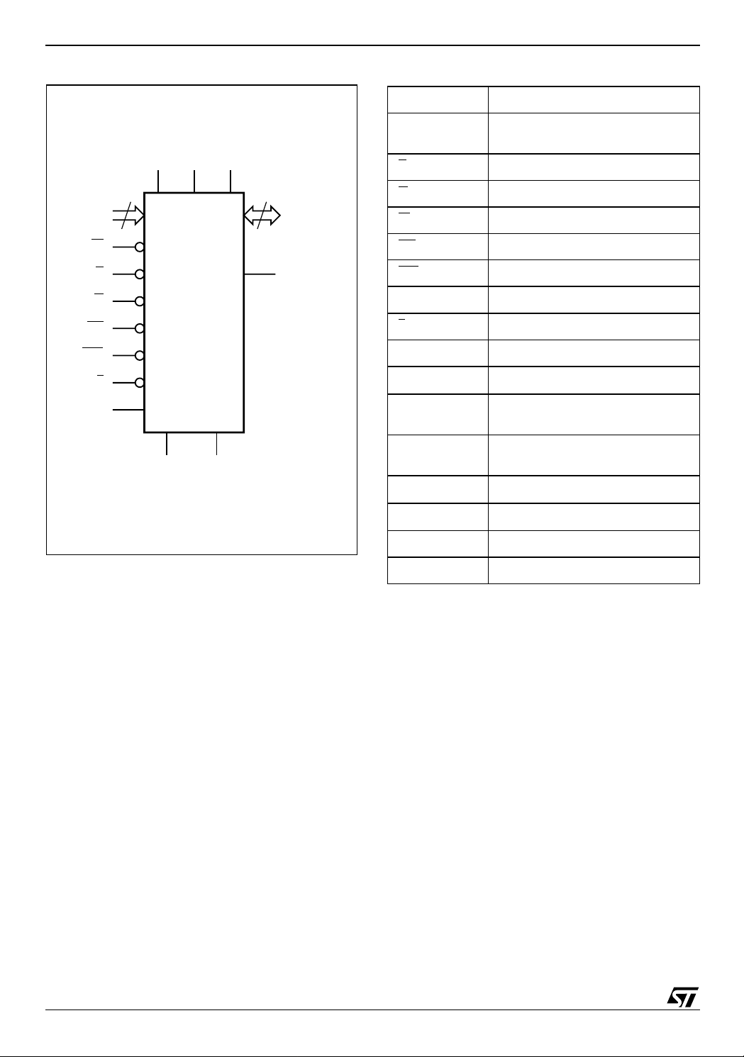
Figure 2. Logic Diagram Table 1. Signal Names
A0-A22 Address Inputs
A0-A22
W
RP
WP
DQ0-DQ15
V
V
DDQVPP
DD
23
16
DQ0-DQ15
E
G
M58WR128ET
M58WR128EB
WAIT
L
K
V
SS
V
SSQ
AI06993
E
G
W
RP
WP
KClock
L
WAIT Wait
V
DD
V
DDQ
V
PP
V
SS
V
SSQ
Data Input/Outputs, Command
Inputs
Chip Enable
Output Enable
Write Enable
Reset
Write Protect
Latch Enable
Supply Voltage
Supply Voltage for Input/Output
Buffers
Optional Supply Voltage for
Fast Program & Erase
Ground
Ground Input/Output Supply
NC Not Connected Internally
DU Do Not Use
8/87
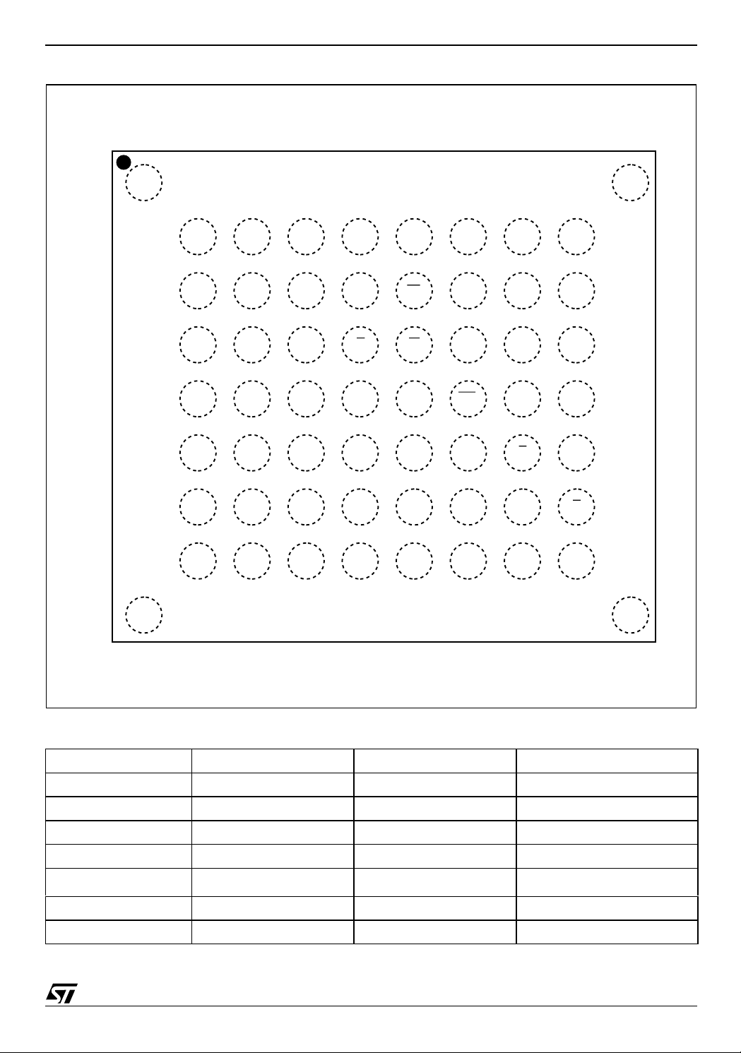
Figure 3. VFBGA Connections (Top view through packa ge)
M58WR128ET, M58WR128EB
87654321
A
B A4
C
D
E
F
G
DU
A13
A15
V
V
DDQ
SS
A8A11
A9A12
A10
A14 WAIT A16 WP
DQ15
DQ14 DQ11 DQ10 DQ9 DQ0 G
V
SS
A20
A21
DQ6
DQ13
V
DD
K RP
L W
DQ4 DQ2 E A0
V
PP
DQ12
A18
DQ1
A6
A5A17
A7A19
A22
A3
A2
A1
9
10
DU
H
J
DU
DQ7 V
SSQ
DQ5 V
DD
DQ3
V
DDQ
DQ8
V
SSQ
Table 2. Bank Architecture
Number Bank Size Parameter Blocks Main Blocks
Parameter Bank 4 Mbits 8 blocks of 4 KWords 7 blocks of 32 KWords
Bank 1 4 Mbits - 8 blocks of 32 KWords
Bank 2 4 Mbits - 8 blocks of 32 KWords
Bank 3 4 Mbits - 8 blocks of 32 KWords
----
Bank 30 4 Mbits - 8 blocks of 32 KWords
Bank 31 4 Mbits - 8 blocks of 32 KWords
----
----
DU
AI07556
----
9/87
M58WR128ET, M58WR128EB
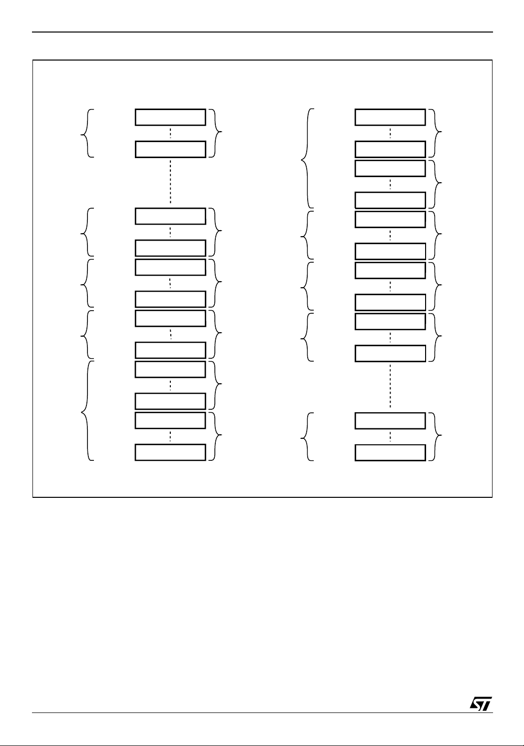
Figure 4. Me m ory Map
Bank 31
Bank 3
Bank 2
Bank 1
Parameter
Bank
M58WR128ET - Top Boot Block
Address lines A22-A0
000000h
007FFFh
038000h
03FFFFh
700000h
707FFFh
738000h
73FFFFh
740000h
747FFFh
778000h
77FFFFh
780000h
787FFFh
7B8000h
7BFFFFh
7C0000h
7C7FFFh
7F0000h
7F7FFFh
7F8000h
7F8FFFh
7FF000h
7FFFFFh
32 KWord
32 KWord
32 KWord
32 KWord
32 KWord
32 KWord
32 KWord
32 KWord
32 KWord
32 KWord
4 KWord
4 KWord
8 Main
Blocks
8 Main
Blocks
8 Main
Blocks
8 Main
Blocks
7 Main
Blocks
8 Parameter
Blocks
Parameter
Bank
Bank 1
Bank 2
Bank 3
Bank 31
M58WR128EB - Bottom Boot Block
Address lines A22-A0
000000h
000FFFh
007000h
007FFFh
008000h
00FFFFh
038000h
03FFFFh
040000h
047FFFh
078000h
07FFFFh
080000h
087FFFh
0B8000h
0BFFFFh
0C0000h
0C7FFFh
0F8000h
0FFFFFh
7C0000h
7C7FFFh
7F8000h
7FFFFFh
4 KWord
4KWord
32 KWord
32 KWord
32 KWord
32 KWord
32 KWord
32 KWord
32 KWord
32 KWord
32 KWord
32 KWord
8 Parameter
Blocks
7 Main
Blocks
8 Main
Blocks
8 Main
Blocks
8 Main
Blocks
8 Main
Blocks
10/87
AI06994

SIGNAL DESCRIPTIONS
See Figure 2 Logic Diagram and Table 1,S ignal
Names, for a brief overview of the signals connected to this device.
Address Inputs (A0-A22). The Address Inputs select the cells i n the memory array to a ccess during Bus Read operations. During Bus Write operations they control the commands sent to the Command Interface of the internal state machine.
Data Input/Output (DQ0-DQ15). The Data I/O outputs the data stored at the selected address during a Bus Read operation or inputs a command or the data to be programmed during a Bus Write operation.
Chip Enable (E
). The Chip Enable input acti-
vates the memory control logic, input buffers, decoders and sense amplifiers. When Chip Enable is
and Reset is at VIH the device is in active
at V
IL
mode. When Chi p E nable i s at V
the memory is
IH
deselected, the outputs are high impedan ce and
the power consumption is reduced to the stand-by
level.
Output Enable (G
). The Output Enable controls
data outputs during the Bus Read operation of the
memory.
Write Enable (W
). The Write Enable controls the
Bus Write operation of the memory’s Command
Interface. The data and address inputs are latched
on the rising edge of Chip Enable or Write Enable
whichever occurs first.
Write Protect (WP
). Write Protect is an input
that gives an additional hardware protection for
each block. When Write Protect is at V
, the Loc k-
IL
Down is enabled and the prote ction status of t he
Locked-Down blocks cannot be changed. When
Write Protect is at V
, the Lock-Down is disabled
IH
and the Locked-Down blocks can be locked or unlocked. (refer to Table 13, Lock Status).
Reset (RP
ware reset of the memory. W hen Reset is at V
). The Reset input provides a hard-
IL
the memory is in reset mode: the outputs are high
impedance and the current consumption is reduced to the Reset Supply Current I
. Refer to
DD2
Table 18, DC Characteristics - Currents for the value of I
After Reset all blocks are in the Locked
DD2.
state and the Configuration Register is reset.
When Reset is at V
, the device is in normal op-
IH
eration. Exiting reset mode the device enters
asynchronous read mod e, b ut a negative transition of Chip Enable or Lat ch E nable is required to
ensure valid data outputs.
The Reset pin can be interfaced with 3V logic without any additional circuitry . It can be tied to V
RPH
(refer to Table 19, DC Characteristics).
Latch Enable (L
). Latch Enable l atches t he ad-
dress bits on its rising edge. The address
latch is transparent when Latch Enable i s a t
M58WR128ET, M58WR128EB
V
and it is inhibited whe n Latch Enable is at
IL
V
. Latch Enable can be kept Low (also at
IH
board level) when t he Latch Enable func tion
is not required o r sup ported.
Clo c k (K). The clock input synchronizes the memory to the microcontroller during synchronous read operations; the address is latched on a Clock edge (rising or falling, according to the configuration settings) when Latch Enable is at V don't care during asynchronous read and in write operations.
Wait (WAIT). Wai t is an output signal used during synchronous read to indicate whether the dat a on the output bus are valid. This output is high impedance when Chip Enable is at V It can be configured to be active during the wait cycle or one clock cycle in advance. The WAIT signal is not gated by Output Enable.
Supply Voltage . VDD provides the power
V
DD
supply to the internal core of the memory device.
It is the main power supply for all operations
(Read, Program and Erase).
Supply Voltage. V
V
DDQ
supply to the I/O pins and enables all Outputs to
be powered independently from V
tied to V
Program Supply Vol t age . VPP is both a
V
PP
or can use a separate supply.
DD
control input and a power supply pin. The two
functions are selected by the voltage range applied to the pin.
is kept in a low voltage range (0V to V
If V
PP
V
is seen as a control input. In this case a volt-
PP
age lower than V
gives an absolute protection
PPLK
against program or erase, whi le V
ables these functions (see Tables 18 and 19, DC
Characteristics for the relevant values). V
sampled at the beginning of a program or erase; a
change in its value after the operation has started
does not have any effect and program or erase op-
,
erations continue.
is in the rang e of V
If V
PP
supply pin. In this condition V
til the Program/Erase algorithm is completed.
V
Ground. VSS ground is the reference for t he
SS
core supply. It must be connected to the system
ground.
V
SSQ
Ground. V
ground is the reference for
SSQ
the input/output circuitry driven by V
must be connected to V
SS
Note: Each device in a system should have
V
DD, VDDQ
and VPP decoupled wi th a 0.1 µF ce-
ramic capacitor close to the pin (high frequency, inherently low inductance capacitors
should be as close as possible to the pack-
or Reset is at VIL.
IH
provides the power
DDQ
. V
DD
PP
it acts as a power
PPH
must be stable un-
PP
. Clock is
IL
DDQ
> V
PP
DDQ
can be
DDQ
en-
PP1
is only
. V
SSQ
)
11/87
M58WR128ET, M58WR128EB
age). See Figure 9, AC Measurement Load Circuit. The PCB track widths should be sufficient
BUS OPERATIONS
There are six standard bus operations that control
the device. These are Bus Read , Bus Write, Address Latch, Output Disable, Standby and Reset.
See Table 3, Bus Operations, for a summary.
Typically glitches of less than 5ns on Chip Enable
or Write Enable are ignored by the memory and do
not affect Bus Write operations.
Bus Read. Bus Read operations are used to output the contents of the Memory Array, the Electronic Signature, the Status Register and the Common Flash Interface. Both Chip Enable and Output Enable must be at V
in order to perform a
IL
read operation. The Chip Enable input s hould be
used to enable the device. Out put Enable should
be used to gate data onto the output. The data
read depends on the previous command written to
the memory (see Command Interface section).
See Figures 10, 1 1, 12 and 13 Read AC Waveforms, and Tables 20 and 21 Read AC Characteristics, for details of when the output becomes
valid.
Bus Write. Bus Write operations write Commands to the memory or latch Input Data to be programmed. A bus write operation is initiated when Chip Enable and Write Enable are at V Output Enable at V
. Commands, Input Data and
IH
IL
with
Addresses are latched on the rising edge of Write
Enable or Chip Enable, whichever occurs first. The
addresses can also be latched prior to the write
operation by toggling Latc h Enable. In this case
to carry the re quired VPP program and erase
currents.
the Latch Enable shoul d be t ied to V
during the
IH
bus write operation.
See Figures 16 and 17, Write AC Waveforms, and
Tables 22 and 23, Write AC Characteristics, for
details of the timing requirements.
Address Latch. Address latch operations input valid addresses. Both Chip enable and Latch Enable must be at V
during address latch opera-
IL
tions. The addresses are latched on the rising
edge of Latch Enable.
Output Disa bl e . The outputs are high impedance when the Output Enable is at V
.
IH
Standby. Standby di sables most of the internal circuitry allowing a substantial reduction of the current consumption. The memory is in stand-by when Chip Enable and Reset are at V
. The pow-
IH
er consumption is reduced to the stand-by level
and the outputs are s et to high impedan ce, independently from the Output Enable or Write Enable
inputs. If Chip Enable switches to V
during a pro-
IH
gram or erase operation, the device enters Standby mode when finished.
Reset. During Reset mode the memory is deselected and the outputs are high impedance. The memory is in Reset mode when Reset is at V
IL
The power consumption is reduced to the Standby
level, independently from the Chip Enable, Output
Enable or Write Enable inputs. If Reset is pulled to
V
during a Program or Erase, this operation is
SS
aborted and the memory content is no longer valid.
.
Table 3. Bus Operations
Operation E G W L RP
Bus Read
Bus Write
Address Latch
Output Disable
Standby
Reset X X X X
Note: 1. X = Don’t care.
2. L
can be tied to VIH if the valid address has been previously latched.
3. Depends on G
4. WAI T signal polarity is configu red using the S et Configuration Register comman d.
12/87
V
IL
V
IL
V
IL
V
IL
V
IH
.
V
IL
V
IH
X
V
IH
XXX
V
IH
V
IL
V
IH
V
IH
(2)
V
IL
(2)
V
IL
V
IL
X
V
IH
V
IH
V
IH
V
IH
V
IH
V
IL
(4)
WAIT
Hi-Z Hi-Z
Hi-Z Hi-Z
DQ15-DQ0
Data Output
Data Input
Data Output or Hi-Z
(3)
Hi-Z
COMMAND INTERFACE
All Bus Write operations t o the me mory are in terpreted by the Command Interface. Commands
consist of one or more sequential Bus Write operations. An internal Program/Erase Controller handles all timings and verifies the correct execution
of the Program and Erase commands. The Program/Erase Controller provides a S tatus Register
whose output may be read at any ti me to monitor
the progress or the result of the operation.
The Command Interface is reset to read mode
when power is first applied, when exiting from Reset or whenever V
is lower than V
DD
LKO
. Command sequences must be followed exactly. Any
invalid combination of commands will be ignored.
Refer to Table 4, Command Codes and Appendix
D, Tables 44, 45, 46 and 47, Command I nterface
States - Modify and Lock Tables, for a summary of
the Command Interface.
The Command Interface is split into two type s of
commands: Standard commands and Factory
Program commands. The following sections explain in detail how to perform each command.
M58WR128ET, M58WR128EB
Table 4. Command Codes
Hex Code Command
01h Block Lock Confirm
03h Set Configuration Register Confirm
10h Alternative Program Setup
20h Block Erase Setup
2Fh Block Lock-Down Confirm
30h Enhanced Factory Program Setup
35h Double Word Program Setup
40h Program Setup
50h Clear Status Register
56h Quadruple Word Program Setup
60h
70h Read Status Register
75h
80h Bank Erase Setup
Block Lock Setup, Block Unlock Setup,
Block Lock Down Setup and Set
Configuration Register Setup
Quadruple Enhanced Factory Program
Setup
90h Read Electronic Signature
98h Read CFI Query
B0h Program/Erase Suspend
C0h Protection Register Program
Program/Erase Resume, Block Erase
D0h
FFh Read Array
Confirm, Bank Erase Confirm, Block
Unlock Confirm or Enhanced Factory
Program Confirm
13/87

M58WR128ET, M58WR128EB
COMMAND INTERFACE - STANDARD COMMANDS
The following commands are the basic commands
used to read, write to and configure the device.
Refer to Table 5, Standard Commands, in conjunction with the following text descriptions.
Read Array Command
The Read Array comm and returns the addressed
bank to Read Array mode. One Bus Write cycle is
required to issue the Read Array command and return the addressed bank to Read Array mode.
Subsequent read operations will read the addressed location and output t he data. A Read Array command can be issued in one bank while
programming or erasing in another bank. However
if a Read Array command is issued to a bank currently executing a Program or Erase operation the
command will be e xecuted but t he output da ta is
not guaranteed.
Read Status Register Command
The Status Register indi cates when a Program or
Erase operation is complete and the success or
failure of operation itself. Issue a Read Status
Register command to read the Status Register
content. The Read Status Register com man d c an
be issued at any time, even during Program or
Erase operations.
The following read operations output the content
of the Status Register of the addressed bank. The
Status Register is latched on the falling edge of E
or G signals, and can be read until E or G returns
. Either E or G must be toggled to update the
to V
IH
latched data. See Table 8 for the description of the
Status Register Bits. This mode supports asynchronous or single synchronous reads only.
Read Electronic Signature Command
The Read Electronic Signature command reads
the Manufacturer and Device Codes, the Block
Locking Status, the Protection Register, and the
Configuration Register.
The Read Electronic Signature command consists
of one write cycle to an address within one o f the
banks. A subsequent Read ope ra tion in the same
bank will output the Manufacturer Code, the Device Code, the protection Status of the blocks in
the targeted bank, the Protection Register, or the
Configuration Register (see Table 6).
If a Read Electronic Signature command is issued
in a bank that is executing a Program or Erase operation the bank will go into Read Electronic Signature mode, subsequent Bus Read cycles will
output the Electronic Sign ature data an d the Pr ogram/Erase controller will continue t o program or
erase in the background. This mode supports
asynchronous or single synchronous reads only, it
does not support page mode or synchronous burst
reads.
Read CFI Query Command
The Read CFI Query command is used to read
data from the Common Flash Interface (CFI). The
Read CFI Query Command consists of one Bus
Write cycle, to an address within one of the banks.
Once the command is issued subsequent Bus
Read operations in the s ame bank read from the
Common Flash Interface.
If a Read CFI Query command is issued in a bank
that is executing a Program or Erase operation the
bank will go into Read CFI Query mo de, s ubsequent Bus Read cycles will output the CFI data
and the Program/Erase con troller will continue to
Program or Erase in the background. This m ode
supports asynchronous or single synchronous
reads only, it does not support page mode or synchronous burst reads.
The status of the other banks is not affected by the
command (see Table 11). After issuing a Read
CFI Query command, a Read Array command
should be issued to t he address ed bank to return
the bank to Read Array mode.
See Appendix B, Common Flash Interface, Tables
34, 35, 36, 37, 38, 39, 40, 41, 42 and 43 for details
on the information contained in the Common Flash
Interface memory area.
Clear Status Register Command
The Clear Status Register comm and c an b e us ed
to reset (set to ‘0’) error bits SR1, SR3, SR4 and
SR5 in the Status Register. One bus write cycle is
required to issue the Clear Status Register command. The Clear Status Register command does
not change the Read mode of the bank.
The error bits in the Status Regi ster do not automatically return to ‘0’ when a new command is issued. The error bits i n the Stat us Register should
be cleared before attempting a new Program or
Erase command.
Block Erase Command
The Block Erase com mand can be used to erase
a block. It sets all the bits within the selected block
to ’1’. All previous d ata in th e block is lost. If th e
block is protected then the Erase operation will
abort, the data in the block will not be changed and
the Status Register will output the error. The Block
Erase command can be issued at any moment, regardless of whether the block has been programmed or not.
Two Bus Write cycles are required to issue the
command.
■ The first bus cycle sets up the Erase command.
■ The second latches the block address in the
internal state machine and starts the Program/
Erase Controller.
14/87

M58WR128ET, M58WR128EB
If the second bus cycle is not Write Erase Confirm
(D0h), Status Register bits SR 4 and SR5 are set
and the command aborts. Erase aborts if Reset
turns to V
. As data integrity cannot be guaran-
IL
teed when the Erase operation is aborted, the
block must be erased again.
Once the command is issued the device outputs
the Status Register data when any address within
the bank is read. At the end o f the operation the
bank will remain in Read Status Register mode until a Read A rray, Read CFI Query o r Read Electronic Signature command is issued.
During Erase operations the bank containing the
block being erased will only accept the Read Array, Read Status Register, Read Electronic Signature, Read CFI Query and the Program/Erase
Suspend command, all other commands will be ignored. Refer to Dual Operations section for detailed information about simultaneous operations
allowed in banks not being e rased. Typical Erase
times are given in Table 14, Program, Erase
Times and Program/Erase Endurance Cycles.
See Appendix C, Figure 26, Block Erase Flowchart and Pseudo Code, for a suggested flowchart
for using the Block Erase command.
Program Command
The memory array can be programmed word-byword. Only one Word in one bank can be programmed at any one time. Two bus write cycles
are required to issue the Program Command.
■ The first bus cycle sets up the Program
command.
■ The second latches the Address and the Data to
be written and starts the Program/Erase
Controller.
After programming has started, read operations in
the bank being programmed output the Status
Register content.
During Program operations the bank being programmed will only accept the Read Array, Read
Status Register, Read Electronic Signature, Read
CFI Query and the Program/Erase Suspend command. Refer to Dual Operations section for detailed information about simultaneous operations
allowed in banks not bei ng programmed. Typical
Program times are given in Table 14, Program,
Erase Times and Program/Erase Endurance Cycles .
Programming aborts if Reset goe s to V
. As data
IL
integrity cannot be guaranteed when the program
operation is aborted, the memory location must be
reprogrammed.
See Appendix C, Figure 22, Program Flowchart
and Pseudo Code, for the f lowchart for using the
Program command.
Program/Erase Suspend Command
The Program/Erase Suspend command is used to
pause a Program or Block Erase operation. A
Bank Erase operation cannot be suspended.
One bus write cycle is required to issue t he Program/Erase command. O nce the Program/Erase
Controller has paused bits SR7, SR6 and/ or SR2
of the Statu s Regist er will be s et to ‘1’. Th e command can be addressed to any bank.
During Program/Erase Suspend the Command Interface will accept the Program/Erase Resume,
Read Array (cannot read the erase-suspended
block or the program-suspended Word), Read
Status Register, Read Electronic Signature and
Read CFI Query commands. Additionally, if the
suspend operation was E rase then the Clear status Register, Program, Block Lock, Block LockDown or Block Unlock commands will also be accepted. The block being erased may be protected
by issuing the Block Lock, Block Lock-Down or
Protection Register Program commands. Only the
blocks not being erased may be read or programmed correctly. When the Program/Erase Resume command is issued the operation will
complete. Refer to the Dual Operations section for
detailed information about simultaneous operations allowed during Program/Erase Suspend.
During a Program/Erase Suspend, the device can
be placed in standby mode by taking Chip Enable
. Program/Erase is aborted if Reset turns to
to V
IH
V
.
IL
See Appendix C, Figure 25 , Program Suspend &
Resume Flowchart and Pseudo Code, and Figure
27, Erase Suspend & Resume Flowchart and
Pseudo Code for flowcharts for using the Program/
Erase Suspend command.
Program/Erase Resu me Command
The Program/Erase Resume command can be
used to restart the Program/Erase Controller after
a Program/Erase Suspen d command has paused
it. One Bus Write cycle is required to issue the
command. The command can be written to any
address.
The Program/Erase R esume command d oes not
change the read m ode of the banks. If the s uspended bank was in Read Status Register, Read
Electronic signature or Read CFI Query mode the
bank remains in that m ode and outputs the corresponding data. If the bank was in Read Array
mode subsequent read operations will output invalid data.
If a Program command is issued d uring a Block
Erase Suspend, then the erase cannot be resumed until the programming operation has completed. It is possible to accumulate suspend
operations. For example: su spend an erase operation, start a programming operation, suspend the
15/87

M58WR128ET, M58WR128EB
programming operation then read the array. See
Appendix C, Figure 25, Program Su spend & Resume Flowchart and Pseudo Code, and Figure 27,
Erase Suspend & Resume Flowchart and Pseudo
Code for flowcharts for using the Program/Erase
Resume command.
Protection Regi ster Program Com m a nd
The Protection Register Program command is
used to Program the 128 bit user O ne-Time-Programmable (OTP) segment of the Protection Register and the Protection Register Lock. The
segment is programmed 16 bits at a time. When
shipped all bits in the segment are set to ‘1’. The
user can only program the bits to ‘0’.
Two write cycles are required to issue the Protection Register Program command.
■ The first bus cycle sets up the Protection
Register Program command.
■ The second latches the Address and the Data to
be written to the Protection Register and starts
the Program/Erase Controller.
Read operations output the Status Register content after the programming has started.
The segment can be protected by programming bit
1 of the Protection Lock Register. Bit 1 of the P rotection Lock Register also protects bit 2 of the Protection Lock Register. Programming bit 2 of the
Protection Lock Register will result in a permanent
protection of Parameter Block #0 (see Figure 5,
Security Block and Protection Register Memory
Map). Attempting to program a previously protected Protection Register will result in a Status Register error. The protection of the Protection
Register and/or the Security Block is not reversible.
The Protection Register Program cannot be suspended. See Appendix C, Figure 29, Protection
Register Program Flowchart and Pseudo Code,
for a flowchart for using the Protection Register
Program command.
Set Conf ig uration Regi s te r Com m and
The Set Configuration Register command is used
to write a new value to the Burst Configuration
Control Register which defines the burst length,
type, X latency, Synchronous/Asynchronous Read
mode and the valid Clock edge configuration.
Two Bus Writ e cycles a re required to i ssue the Set
Configuration Register command.
■ The first cycle writes the setup command and
the address corresponding to the Configuration
Register content.
■ The second cycle writes the Configuration
Register data and the confirm command.
The Read mode of the banks is not modified when
the Set Configuration Register command is issued.
The value for the Configuration Register is always
presented on A0-A15. CR0 is on A0, CR1 on A1,
etc.; the other address bits are ignored.
Block Lock Command
The Block Lock command is used to lock a block
and prevent Program or Erase operations from
changing the data in it. All blocks are locked at
power-up or reset.
Two Bus Write cycles are required to issue the
Block Lock command.
■ The first bus cycle sets up the Block Lock
command.
■ The second Bus Write cycle latc hes the block
address.
The lock status can be monitored for each block
using the Read Electronic Signature command.
Table. 13 shows the Lock Status after issuing a
Block Lock command.
The Block Lock bits are vo latile, once set they remain set until a hardware reset or power-down/
power-up. They are cleared by a Block Unlock
command. Refer to the section, Block Locking, for
a detailed explanation. See Appendix C, Figure
28, Locking Operations Flowchart and Pseudo
Code, for a flowchart for using the Lock command.
Block Unlock Command
The Block Unlock command is used to unlock a
block, allowing the block to be programmed or
erased. Two Bus Write cycles are requ ired to issue the Block Unlock command.
■ The first bus cycle sets up the Block Unlock
command.
■ The second Bus Write cycle latc hes the block
address.
The lock status can be monitored for each block
using the Read Electronic Signature command.
Table 13 shows the protection status after issuing
a Block Unlock command. Refer to the section,
Block Locking, for a detailed expla nation and A ppendix C, Figure 28, Locking Operations Flowchart and Pseudo Code, f or a flowchart for using
the Unlock command.
Block Lock-Down Command
A locked or unlocked block can be locked-down by
issuing the Block Lock-Down command. A lockeddown block cannot be programm ed or erased, or
have its protection status changed when WP
low, V
. When WP is high, V
IL
the Lock-Down
IH,
is
function is disabled and the locked blocks can be
individually unlocked by the Block Unlock command.
Two Bus Write cycles are required to issue the
Block Lock-Down command.
■ The first bus cycle sets up the Block Lock
command.
16/87

M58WR128ET, M58WR128EB
■ The second Bus Write cycle latc hes the blo ck
address.
The lock status can be monitored for each block
using the Read Electronic Signature command.
Locked-Down blocks revert to the locked (and not
locked-down) state when the device is reset on
power-down. Table. 13 shows the Lo ck Statu s after issuing a Block Lock-Down command. Refer to
the section, Block Locking, for a detailed explanation and Appendix C, Fi gure 28, Locking Operations Flowchart and Pseudo Code, for a flowchart
for using the Lock-Down command.
Table 5. Standard Commands
Bus Operations
Commands
Cycles
Read Array 1+ Write BKA FFh
Read Status Regist er 1+ Write BKA 70h Read
Read Electronic Signature 1+ Write BKA 90h Read
Read CFI Query 1+ Write BKA 98h Read
Clear Status Register 1 Write BKA 50h
Block Erase 2 Write
Program 2 Write
Program/E rase Su s pen d 1 Wri te X B0h
Program/Erase Resume 1 Write X D0h
Protection Register Program 2 Write PRA C0h Write
Set Configuration Register 2 Write CRD 60h Write
Block Lock 2 Write
Block Unlock 2 Write
Block Lock-Down 2 Write
Note: 1. X = Don’t Care, WA=Word Address in targeted bank, RD=Read Data, SRD=Status Register Data, ESD=Electronic Signature Data,
QD=Query Dat a, BA=Bl ock Address, BK A= Ban k Address , PD= Program Data, PR A=Prot ectio n Regist er Addre ss, PRD =Prote ction
Register Dat a, CRD=Configurat i on Register Data.
2. Mus t be same bank as in the first cycle. The signat ure address es are listed i n T able 6.
3. Any address wit hi n the bank ca n be used.
Op. Add Data Op. Add Data
1st Cycle 2nd Cycle
BKA or BA
BKA or
(3)
WA
Read
(3)
20h Write BA D0h
40h or 10h Write WA PD
WA RD
BKA
BKA
BKA
PRA PRD
CRD
(3)
BKA or BA
BKA or BA
BKA or BA
60h Write BA 01h
(3)
60h Write BA D0h
(3)
60h Write
BA
(2)
(2)
(2)
SRD
ESD
QD
03h
2Fh
17/87
M58WR128ET, M58WR128EB
Table 6. Electronic Signature Codes
Code Address (h) Dat a (h)
Manufacturer Code Bank Address + 00 0020
Device Code
Top Bank Address + 01 881E
Bottom Bank Address + 01 881F
Locked
0001
Unlocked 0000
Block Protection
Block Address + 02
Locked and Locked-Down 0003
Unlocked and Locked-Down 0002
Reserved Bank Address + 03 Reserved
Configuration Register Bank Address + 05 CR
ST Factory Default
0006
Security Block Permanently Locked 0002
Protection Register Lock
OTP Area Permanently Locked 0004
Security Block and OTP Area Permanently
Locked
Bank Address + 80
Bank Address + 81
Bank Address + 84
0000
Unique Device
Number
Protection Register
Bank Address + 85
Bank Address + 8C
Note: CR=Config uration Regi ster.
OTP Area
Figure 5. Security Block and Protection Register Memory Map
18/87
SECURITY BLOCK
Parameter Block # 0
8Ch
85h
84h
81h
80h
PROTECTION REGISTER
User Programmable OTP
Unique device number
Protection Register Lock 2 1 0
AI06181

COMMAND INTERFACE - FACTORY PROGRAM COMMANDS
The Factory Program commands are used to
speed up programming. They require V
V
except for the Bank Eras e command which
PPH
also operates at V
= VDD. Refer to Table 7, Fac-
PP
to be at
PP
tory Program Commands, in conjunction with the
following text descriptions.
The use of the Factory Program commands require certain operating conditions:
■ V
must be set t o V
PP
(except for Bank Erase
PPH
command)
■ V
must be within operating range
DD
■ Ambient temperature, T
■ The targeted block must be unlocked
must be 25°C ± 5°C
A
Refer to Table 7, Factory Program Comm ands , in
conjunction with the following text descriptions.
Bank Erase Command
The Bank Erase command can be used to erase a
bank. It sets all the bits within the selected bank to
’1’. All previous data in th e ban k is lo st. Th e B ank
Erase command will igno re any protected blocks
within the bank. If all blocks in the ba nk are protected then the Bank Erase operation will abort
and the data in the bank wi ll not b e changed. The
Status Register will not output any error.
Bank Erase operations can be p erformed at both
V
PP
= V
and VPP = VDD.
PPH
Two Bus Write cycles are required to issue the
command.
■ The first bus cycle sets up the Bank Erase
command.
■ The second latches the bank address in the
internal state machine and starts the Program/
Erase Controller.
If the second bus cycle is not Write Bank Erase
Confirm (D0h), Status Register bits SR4 and S R5
are set and the command aborts. Erase aborts if
Reset turns to V
. As data integrity cannot be
IL
guaranteed when the Erase operation is aborted,
the bank must be erased again.
Once the command is issued the device outputs
the Status Register data when any address within
the bank is read. At the end o f the operation the
bank will remain in Read Status Register mode until a Read Array, Read CFI Query or Read Electronic Signature command is issued.
During Bank Erase operations the bank being
erased will only accept the Read Array, Read Status Register, Read Electronic Signature and Read
CFI Query command, all other commands will be
ignored.
For optimum performance, Bank Erase commands should be limited to a maximum of 100 Program/Erase cycles per Block. After 100 Program/
properly but some degradation in performance
may occur.
Dual operations are not supported during Bank
Erase operations and the command cannot be
suspended.
Typical Erase times are given in Table 14, Program, Erase Times and Program/Erase Endurance Cycles.
Double Word Program Command
The Double Word Program command improves
the programming throughput by writing a page of
two adjacent words in parallel. The two words
must differ only for the address A0.
Three bus write cycles are neces sary to issue the
Double Word Program command.
■ The first bus cycle sets up the Double Word
Program Command.
■ The second bus cycle latches the Address and
the Data of the first word to be written.
■ The third bus cycle latches the Address and the
Data of the second word to be written and starts
the Program/Erase Controller.
Read operations in the bank bei ng programmed
output the Status Register content after the programming has started.
During Double Word Program operations the bank
being programmed will only accept the Read Array, Read Status Register, Read Electronic Signature and Read CFI Query command, all other
commands will be ignored. Dual operations are
not supported during Double Word Program operations and the command cannot be suspended.
Typical Program times are given in Table 14, Program, Erase Times and Program/Erase Endurance Cycles.
Programming aborts if Reset goe s to V
integrity cannot be guaranteed when the program
operation is aborted, the memory locations m ust
be reprogrammed.
See Appendix C, Figure 23, Double Word Program Flowchart and Pseudo Code, for the flowchart for using the Double Word Program
command.
Quadruple Word Program Command
The Quadruple Word Program command improves the programming throughput by writing a
page of four adjacent words in parallel. The four
words must differ only for the addresses A0 and
A1.
Five bus write cycles are necessary to issue the
Quadruple Word Program command.
■ The first bus cycle sets up the Double Word
Program Command.
Erase cycles the internal algorithm will still operate
M58WR128ET, M58WR128EB
. As data
IL
19/87

M58WR128ET, M58WR128EB
■ The second bus cycle latches the Address and
the Data of the first word to be written.
■ The third bus cycle latches the Address and the
Data of the second word to be written.
■ The fourth bus cycle latches the Address and
the Data of the third word to be written.
■ The fifth bus cycl e latches the Address and the
Data of the fourth word to be written and starts
the Program/Erase Controller.
Read operations to the bank being programmed
output the Status Register content after the programming has started.
Programming aborts if Reset goe s to V
. As data
IL
integrity cannot be guaranteed when the program
operation is aborted, the memory locations mu st
be reprogrammed.
During Quadruple Word Program operations the
bank being programmed will only accept the Read
Array, Read Status Register, Read Electronic Signature and Read CFI Query command, all other
commands will be ignored.
Dual operations are not supported during Quadruple Word Program operations and the command
cannot be suspended . Typical Program times are
given in Table 14, Program, Erase Times and Program/Erase Endurance Cycles.
See Appendix C, Figure 24, Quadruple Word Program Flowchart and Pseudo Code, for the flowchart for using the Quadruple Word Program
command.
Enhanced Factory Program Command
The Enhanced Factory Program command can be
used to program large streams of dat a within any
one block. It greatly reduces the total programming time when a large number of Words are written to a block at any one time.
Dual operations are not s upported during the Enhanced Factory Program operation an d the command cannot be suspended.
For optimum performance the Enhanc ed Factory
Program commands should be limited to a maximum of 10 program/erase cycles per block. If this
limit is exceeded the in ternal algorithm will cont inue to work properly but some degradation in performance is possible. Typical Prog ram times are
given in Table 14.
The Enhanced Factory Program command has
four phases: the Setup Phase, the Program Phase
to program the data to the memory, the Verify
Phase to check that the data has been correctly
programmed and reprogram if necessary a nd the
Exit Phase. Refer to Table 7, Enhanced Factory
Program Command and Figure 30, Enhanced
Factory Program Flowchart.
Setup Phase. The Enhanced Factory Program
command requires two Bus Write operations to initiate the command.
■ The first bus cycle sets up the Enhanced
Factory Program command.
■ The second bus cycle confirms the command.
The Status Register P/E.C. Bit SR7 should be
read to check that the P/E.C. is ready. After the
confirm command is issued, read operations
output the Status Register data. The read Status
Register command must not be issued as it will be
interpreted as data to program.
Program Phase. The Program Phase requires
n+1 cycles, wher e n is the n umber of Words (refer
to Table 7, Enhanced Factory Program Command
and Figure 30, Enhanced Factory Program Flowchar t).
Three successive steps are required to issue and
execute the Program Phase of the command.
1. Us e one Bus Write operation to latch the Start
Address and the first Word to be programmed.
The Status Register Bank Write Status bit SR0
should be read to check that the P/E.C. is ready
for the next Word.
2. Each subsequent Word to be programmed is
latched with a new Bus Write operation. The
address can either remain the Start Address, in
which case the P/E.C. increments the address
location or the address can be incremented in
which case the P/E.C. jumps to the new
address. If any address that is not in the same
block as the Start Address is given with data
FFFFh, the Program Phase terminates and the
Verify Phase begins. The Status Register bit
SR0 should be read between each Bus Write
cycle to check that the P/E.C. is ready for the
next Word.
3. Finally, after all Words have been programmed,
write one Bus Write operation with data FFFF h
to any address outside the bl ock contain ing the
Start Address, to terminate the programming
phase. If the data is not FFFFh, the command is
ignored.
The memory is now set to enter the Verify Phase.
Verify Phase. Th e Verify Phase is s imilar to the
Program Phase in that all Words must be resent to
the memory for them to be che cked against the
programmed data. The Program/Erase Controller
checks the stream of da ta with the data that was
programmed in the Program Phase and reprograms the memory location if necessary.
Three successive steps are required to execute
the Verify Phase of the command.
1. Us e one Bus Write operation to latch the Start
Address and the first Word, to be verified. The
Status Register bit SR0 should be read to check
20/87

M58WR128ET, M58WR128EB
that the Program/Erase Controller is ready for
the next Word.
2. Each subsequent Word to be verified is latched
with a new Bus Write operation. The Words
must be written in the same order as in the
Program Phase. The address can remain the
Start Address or be incremented. If any address
that is not in the same block as the Start
Address is given with data FFFFh, the Verify
Phase terminates. Status Register bit SR0
should be read to check that the P/E.C. is ready
for the next Word.
3. Finally, after all Words have been verified, write
one Bus Write operation with data FFFFh to any
address outside the block containing the Start
Address, to terminate the Verify Phase.
If the Verify Phase is successfully completed the
memory remains in Read Status Register mode. If
the Program/Erase Controller fails to reprogram a
given location, the error will be signaled in the Status Register.
Exit Phase. Status Register P/E.C. bit SR7 set to
‘1’ indicates that the device has ret urned to Read
mode. A full Status Register check should be done
to ensure that the block has been successfully programmed. See the s ect ion on the Status Register
for more details.
Quadruple Enhanced Factory Program Command
The Quadruple Enhanced Factory Program command can be used to program one or more pages
of four adjacent words in parallel. The four words
must differ only for the addresses A0 and A1.
Dual operations are not supported during Quadruple Enhanced Factory Program operations and
the command cannot be suspended.
It has four phases: the Setup Phase, the Load
Phase where the data is loaded into the buffer, the
combined Program and Verify Phase where the
loaded data is programmed to the memory and
then automatically checked and reprogrammed if
necessary and the Exit Phase. Unlike the Enhanced Factory Program it is not necess ary t o resubmit the data for the Verify Phase. The Load
Phase and the Program and Verify Phas e can be
repeated to program any number of pag es within
the block.
Setup Phase. The Q uadruple Enhan ced Factory
Program command requires one Bus Write operation to initiate the load phase. After the setup
command is issued, read operations output the
Status Register data. The Read Status Register
command must not be issued as it will be
interpreted as data to program.
Load Phase. The Load Phase requires 4 cycles
to load the data (refer to Table 7, Factory Program
Commands and Figure 31, Quadruple Enhanced
Factory Program Flowchart). Once the first Word
of each Page is written it is impossible to exit the
Load phase until all four Words have been written.
Two successive steps are required to issue and
execute the Load Phase of the Quadruple Enhanced Factory Program comm and.
1. Us e one Bus Write operation to latch the Start
Address and the first Word of the first Page to
be programmed. For subsequent Pages the first
Word address can remain the Start Address (in
which case the next Page is programmed) or
can be any address in the same block. If any
address with data FFFFh is given that is not in
the same block as the Start Address, the device
enters the Exit Phase. For the first Load Phase
Status Register bit SR7 should be read after the
first Word has been issued to check that the
command has been accepted (bit 7 set to ‘0’).
This check is not required for subsequent Load
Phases.
2. Each subsequent Word to be programmed is
latched with a new Bus Write operation. The
address is only checked for the first Word of
each Page as the order of the Words to be
programmed is fixed.
The memory is now set to enter the Program and
Verify Phas e .
Program and Verify Phase. In the Program and
Verify Phase the four Words that were loaded in
the Load Phase are programmed in the memory
array and then verified by the Program/Erase Controller. If any errors are found the Program/Erase
Controller reprograms the location. During this
phase the Status Register shows that the Program/Erase Controller is busy, Status Register bit
SR7 set to ‘0’, and that the device is not waiting for
new data, Status Register bit SR0 set to ‘1’. When
Status Register bit SR0 i s set to ‘0’ the Program
and Verify phase has terminated.
Once the Verify Phase has successfully completed subsequent pages in the same block can be
loaded and programmed. The device returns to
the beginning of the Load Phase by issuing one
Bus Write operation to latch the A ddress and the
first of the four new Words to be programmed.
Exit Phase . Finally, after all the pages have been
programmed, write one Bus Write operation with
data FFFFh to any address outside the block containing the Start Address, to terminate the Load
and Program and Verify Phases.
A full Status Register check should be done to ensure that the block has been sucessfully programmed. See the s ect ion on the Status Register
for more details.
If the Program and Verify Phase has successfully
completed the memory returns to Read mode. If
the P/E.C. fails to program and reprogram a given
21/87
M58WR128ET, M58WR128EB
location, the error will be signaled in the Status
Register.
Table 7. Factory Program Commands
Command Ph ase
Cycles
Bank Erase 2 BKA 80h BKA D0h
1st 2nd 3rd Final -1 Final
Add Data Add Data Add Data Add Data Add Data
Bus Write Operations
Double Word Program
Quadruple Word Program
Enhanced
Factory
Program
(6)
(4)
Setup,
Program
Verify, Exit n+1
Setup,
first Load
(5)
3
5
2+n
+1
5
BKA or
(8)
WA1
BKA or
(8)
WA1
BKA or
(8)
WA1
(2)
WA1
BKA or
(8)
WA1
35h WA1 PD1 WA2 PD2
56h WA1 PD1 WA2 PD2 WA3 PD3 WA4 PD4
30h
PD1
75h
BA or
WA1
WA2
WA1
(9)
(3)
(2)
WA1
WA3
WA2
(2)
(3)
(7)
PD1
PD3
PD2
D0h
PD2
PD1
WAn
WAn
WA3
(3)
(3)
(7)
PAn
PAn
PD3
NOT
WA1
NOT
WA1
WA4
First
Quadruple
Enhanced
Factory
Program
(5,6)
Program &
Verify
Subsequent
Loads
Subsequent
Program &
Automatic
WA1i
4
(2)
PD1i
WA2i
(7)
PD2i
WA3i
(7)
PD3i
Automatic
WA4i
(7)
Verify
NOT
Exit 1
Note: 1. WA=Wo rd Address in t argeted bank, BKA= B an k Address, PD=Pr o gram Data, BA=Block Addres s.
2. WA1 is the Start Address. NOT WA1 is any address that is not in the same block as WA1.
3. Address can rem ai n Starting Address WA1 or be i ncremented.
4. Word Addresses 1 and 2 must be co nsecutive Addresses di f fering only for A0.
5. Word Addresses 1, 2,3 and 4 must be consecut i ve Addresses differing only for A0 and A1.
6. A B us R ead must b e done b etwe en each Wri te c ycle wh ere the dat a is prog ra mmed or veri fied t o rea d the St atus Reg ist er an d
check that the memory is ready to accept the next data. n = number of Wo rds, i = number of Pages to be programmed .
7. Addre ss i s only c heck ed for the fir st Wo rd o f each Page a s the o rde r to pro gr am the Wo rd s in ea ch pag e is fi xed so subs equ ent
Words in each Page can be written to any address.
8. Any address wit hi n the bank ca n be used.
9. Any address withi n the block c an be used.
WA1
FFFFh
(2)
(2)
(2)
(7)
FFFFh
FFFFh
PD4
PD4i
22/87

STATUS REGISTER
The Status Register provides information on the
current or previous Program or Erase operations.
Issue a Read Status Register command to read
the contents of the Status Register, refer to Read
Status Register Command section for more details. To output the contents, the Status Register is
latched and updated on the falling edge of the
Chip Enable or Output Enable signal s and c an be
read until Chip Enable or Output Enable returns to
V
. The Status Register can only be read using
IH
single asynchronous or single synchronous reads.
Bus Read operations from any address within the
bank, always read the Status Register during Program and Erase operations.
The various bits convey information about the status and any errors of the operation. Bits SR7, SR6,
SR2 and SR0 give information on the status of the
device and are set and reset by the device. Bits
SR5, SR4, SR3 and S R1 give information on errors, they are set by the device but must be reset
by issuing a Clear Status Register command or a
hardware reset. If an error bit is set to ‘1’ the Status
Register should be reset before issuing another
command. SR7 to SR1 ref er to the status of the
device while SR0 refers to the status of the addressed bank.
The bits in the Status Register are summarized in
Table 8, Status Register Bits. Refer to Table 8 in
conjunction with the following text descriptions.
Program/Erase Controller Status Bit (SR7). The
Program/Erase Controller Status bit indicates
whether the Program/Erase Controller is act ive or
inactive in any bank. When the Program/Erase
Controller Status bit is Low (set to ‘0’), the Program/Erase Controller is active; when the bit is
High (set to ‘1’), the Program/Erase Controller is
inactive, and the device is ready to process a new
command.
The Program/Erase Controller Status is Low immediately after a Program/Erase Suspend command is issued until the Program/Erase Controller
pauses. After the Program/Erase Controller pauses the bit is High.
During Program, Erase, o perations the Program/
Erase Controller Status bit can be polled to find the
end of the operation. Other bits in the Status Register should not be tested until the Program/Erase
Controller completes the operation and the bit is
High.
After the Program/Erase Cont roller completes its
operation the Erase Status, Prog ram Status, V
PP
Status and Block Lock Status bits should be tested
for errors.
Erase Suspend Status Bit (SR6). The Erase
Suspend Status bit indicates that an Erase operation has been suspended or is going to be sus-
M58WR128ET, M58WR128EB
pended in the addressed block. When the Eras e
Suspend Status bit is High (set to ‘1’), a Program/
Erase Suspend command has been issued and
the memory is waiting for a Program/Erase Resume command.
The Erase Suspend Status should only be considered valid when the Program/Erase Controller Status bit is High (Program/Erase Controller inactive).
SR7 is set within the Erase Suspend Latency time
of the Program/Erase Suspend command being
issued therefore the memory may still complete
the operation rather than entering the Suspend
mode.
When a Program/Erase Re sume command is issued the Erase Suspend Status bit returns Low.
Erase Status Bit (SR5). The Erase Status bit
can be used to identify if the memory has failed to
verify that the block or bank has erased correctly.
When the Erase Status b it is High (set to ‘1’), the
Program/Erase Controller has applied the maximum number of pulses to the block or bank and
still failed to verify that it has erased correctly. The
Erase Status bit should be read once the Program/
Erase Controller Status bit is High (Program/Erase
Controller inactive).
Once set High, the Erase Status bit can only be reset Low by a Clear Status Register command or a
hardware reset. If set High it should be reset before a new Program or Erase command is issued,
otherwise the new command will appear to fail.
Program Status Bit (SR4). The Program Status
bit is used to identify a Program failure or an attempt to program a '1' to an already program med
bit when V
PP
= V
When the Program Status bit is High (set to ‘1’),
the Program/Erase Controller has applied the
maximum number of pulses to the byte an d still
failed to verify that it has programmed correctly.
After an attempt to program a '1' to an already programmed bit, the Program Status bit SR4 goes
High (set to '1') only if V
ent from V
PPH
the attempt is not shown.
The Program St atus bit should be read once t he
Program/Erase Controller Status bit is High (Program/Erase Controller inactive).
Once set High, the Program Status bit can only be
reset Low by a Clear Status Register command or
a hardware reset. If set High it should be reset before a new command is issued, otherwise the new
command will appear to fail.
Status Bit (SR3). The VPP Status bit can be
V
PP
used to identify an invalid v oltage on the V
during Program and Erase operations. The V
pin is only sampled at the beginning of a Program
.
PPH
PP
= V
. If VPP is differ-
PPH
, SR4 remains L ow (set to '0') and
pin
PP
PP
23/87

M58WR128ET, M58WR128EB
or Erase operation. Indeterminate results can occur if V
When the V
age on the V
when the V
becomes invalid during an operation.
PP
Status bit is Low (set to ‘0’), the volt-
PP
pin was sampled at a valid voltage;
PP
Status bit is High (set to ‘1’), the V
PP
PP
pin has a voltage that is below the VPP Lockout
Voltage, V
, the memory is protected and Pro-
PPLK
gram and Erase operations cannot be performed.
Once set High, the V
Status bit can only be reset
PP
Low by a Clear Status Register command or a
hardware reset. If set High it should be reset before a new Program or Erase command is issued,
otherwise the new command will appear to fail.
Program Suspend Status Bit (SR2). The Program Suspend Status bit indicates that a Program
operation has been suspended in the addressed
block. When the Program Suspend Status bit is
High (set to ‘1’), a Program/Erase Suspend command has been issued and the memory is waiting
for a Program/Erase Resume command. The Program Suspend Status should only be considered
valid when the Program/Erase Controller Status
bit is High (Program/Erase Controller inactive).
SR2 is set within t he Program Suspend Latency
time of the Program/Erase Suspend command being issued therefore the memory may still complete the operation rather than entering the
Suspend mode.
When a Program/Erase Re sume command is issued the Program Suspend Status bit returns Low.
Block Protection Status Bit (SR1). The Block
Protection Status bit can be used to identify if a
Program or Block Erase operation has tried to
modify the contents of a locked block.
When the Block Protection Status bit is High (set
to ‘1’), a Program or Erase operation has been attempted on a locked block.
Once set High, the Block Protection Status bit can
only be reset Low by a Clear Status Register command or a hardware reset. If set High it should be
reset before a new command is issued, otherwise
the new command will appear to fail.
Bank Wri te/Multiple Wor d Program Sta tus Bit
(SR0). The Bank Write Status bit indicates wheth-
er the addressed bank is programming or erasing.
In Enhanced Factory Program mode th e Multiple
Word Program bit shows if a Word has finished
programming or verifying depending on the phase.
The Bank Write Status bit should only be considered valid when the Pro gr a m/Erase Controller Status SR7 is Low (set to ‘0’).
When both the Pro gra m/Erase Controller Status bit
and the Bank Write Status bit are Low (set to ‘0’),
the addressed bank is executing a Program or
Erase operation. When the Program/Erase Controller Status bit is Low (set to ‘0’) and the Bank
Write Status bit is High (set to ‘1’), a Program or
Erase operation is being executed in a bank other
than the one being addressed.
In Enhanced Factory Program mode if Multiple
Word Program Status bit is Low (set to ‘0’), the device is ready for the next Word, if the Multiple Word
Program Status bit is High (set to ‘1’) the device is
not ready for the next Word.
Note: Refer to Appendix C, Flowcharts and Ps eudo Codes, for using the Status Register.
24/87
M58WR128ET, M58WR128EB
Table 8. Status Register Bits
Bit Name T ype Logic Level Definition
SR7 P/E.C. Status Status
SR6 Erase Suspend Status Status
’1’ Ready
’0’ Busy
’1’ Erase Suspended
’0’ Erase In progress or Completed
SR5 Erase Status Error
SR4 Program Status Error
SR3
V
PP
Error
Status
SR2 Program Suspend Status Status
SR1 Block Protection Status Error
Bank Write Status Status
SR0
Multiple Word Program
Status (Enhanced
Status
Factory Program mode)
Note: Logic level ’1’ is High, ’0’ is Low.
’1’ Erase Error
’0’ Erase Success
’1’ Program Error
’0’ Program Success
Invalid, Abort
’1’
’0’
V
PP
V
OK
PP
’1’ Program Suspended
’0’ Program In Progress or Completed
’1’ Program/Erase on protected Block, Abort
’0’ No operation to protected blocks
SR7 = ‘0’ Program or erase operation in addressed bank
’0’
SR7 = ‘1’ No Program or erase operation in the device
'1'
SR7 = ‘0’
Program or erase operation in a bank other than
the addressed bank
SR7 = ‘1’ Not Allowed
SR7 = ‘0’ the device is NOT ready for the next word
'1'
SR7 = ‘1’ Not Allowed
SR7 = ‘0’ the device is ready for the next Word
'0'
SR7 = ‘1’ the device is exiting from EFP
25/87

M58WR128ET, M58WR128EB
CONFIGURATION REGISTER
The Configuration Register is used to configure
the type of bus access that the memory will perform. Refe r to Rea d Mo des secti on fo r d etai ls on
read operations.
The Configuration Register is set through the
Command Interface. After a Reset or Power-Up
the device is configured for asynchronous page
read (CR15 = 1). T he Configuration Register bits
are described in Table 9. They spe cify the selection of the burst length, burst type, burst X latency
and the Read operation. Refer to Figures 6 and 7
for examples of synchronous burst configurations.
Read Select Bit (CR15)
The Read Select bit, CR15, is used to switch between asynchronous an d sync hronous B us Read
operations. When the Read Se lect bit is set to ’1’,
read operations are asynchronous; when the
Read Select bit is set to ’0’, read o perations are
synchronous. Synchronous Burst Read is supported in both parameter and main blocks and can be
performed across banks.
On reset or power-up the Read Sel ect bi t is set
to’1’ for asynchronous access.
X-Latency Bits (CR13-CR11)
The X-Latency bits are used during Synchronous
Read operations to set the number of clock cycles
between the address bei ng latched and the first
data becoming available. For correct operation the
X-Latency bits can only assume the values in Table 9, Configuration Register.
The correspondence be tween X-Latency settings
and the maximum sustainable freq uency must be
calculated taking into account some system parameters. Two conditions must be satisfied:
1. Depending on whether t
AVK_CPU
or t
supplied either one of the following two
equations must be satisfied:
(n + 1) t
(n + 2) tK ≥ t
≥ t
K
ACC
ACC
- t
AVK_CPU
+ t
DELAY
+ t
+ t
QVK_CPU
QVK_CPU
2. and also
> t
t
K
KQV
+ t
QVK_CPU
where
n is the chosen X-Latency configuration code
is the clock period
t
K
t
AVK_CPU
is clock to address valid, L Low, or E
Low, whichever occurs last
t
is address valid, L Low, or E Low t o clock,
DELAY
whichever occurs last
t
QVK_CPU
is the data setup time required by the
system CPU,
is the clock to data valid time
t
KQV
is the random access time of the device.
t
ACC
DELAY
is
Refer to Figure 6, X-Latency and Data Output
Configuration Example.
Wait Polarity Bit (CR10)
In synchronous burst mode the W ait signal indicates whether the output data are valid or a WAIT
state must be inserted. The Wait Polarity bit is
used to set the po larity of the Wait signal. When
the Wait Polarity bit is set to ‘0’ the Wait signal is
active Low. When the Wait P ola rity bit is s et t o ‘ 1’
the Wait signal is active High (default).
Data Output Configuration Bit (CR9)
The Data Output Configuration bit determines
whether the output remains valid for one or two
clock cycles. When the Data Output Configuration
Bit is ’0’ the output data is valid for one clock cycle,
when the Data Output Configuration Bit is ’1’ the
output data is valid for two clock cycles.
The Data Output Configuration depends on the
condition:
■ t
> t
K
where tK is the clock period, t
setup time required by the s ystem CPU and t
KQV
+ t
QVK_CPU
QVK_CPU
is the data
KQV
is the clock to data valid time. If this condition is not
satisfied, the Data Output Configuration bit should
be set to ‘1’ (two clock cycles). Refer to Figure 6,
X-Latency and Data Output Configuration Example.
Wait Confi guration Bit (C R 8)
In burst mode the Wait bit controls the timing of the
Wait output pin, WAIT. When WAIT is asserted,
Data is Not Valid and when WAIT is deasserted,
Data is Valid. When the Wait bit is ’0’ the Wait output pin is asserted during the wait state. When the
Wait bit is ’1’ (default) the Wait output pin is asserted one clock cycle before the wait state.
Burst Type Bit (CR7)
The Burst Type bit is used to configure the sequence of addres ses read as sequential or interleaved. When the Burst Type bit is ’0’ the memory
outputs from interleaved addresses; when the
Burst Type bit is ’1’ (default) the mem ory outputs
from sequential addresses. Se e Tables 10, Burst
Type Definition, for the sequence of addresses
output from a given starting address in each mode.
Valid Clock Edge Bit (CR6)
The Valid Clock Edge bit, CR6, is used to configure the active edge of the Clock, K, during Synchronous Burst Read operations. When the Valid
Clock Edge bit is ’0’ the falling edge of the Clock is
the active edge; when the Vali d Clock Edge bit is
’1’ the rising edge of the Clock is active.
Wrap Burst Bit (CR3)
The burst reads can be confined inside the 4 or 8
Word boundary (wrap) or o vercome t he b oundary
26/87

M58WR128ET, M58WR128EB
(no wrap). The Wrap Burst bit i s used to select between wrap and no wrap. When the Wrap Burst bit
is set to ‘0’ the burst read wraps; when it is set to
‘1’ the burst read does not wrap.
Burst length Bits (CR2-CR0)
The Burst Length bits set the n umb er of Words t o
be output during a Synchronous Burst Read operation as result of a single address latch cycle.
They can be set for 4 words, 8 words, 16 words or
continuous burst, where all the words are read sequentially.
In continuous burst mode the burs t sequ ence c an
cross bank boundaries.
In continuous burst mode, in 4, 8 words no-wrap,
or in 16 words, depending on the starting address,
the device asserts the WAIT output to indicate that
a delay is necessary before the data is output.
If the starting address is aligned to a 4 word
boundary no wait states are needed and the WAIT
output is not asserted.
If the starting address is shifted by 1, 2 or 3 pos itions from the four word boundary, WAIT will be
asserted for 1, 2 or 3 clock cycles when the burst
sequence crosses the first 64 word boundary, or
the 16 word boundary in the case of 16-word wrap
burst, to indicate that the device needs an internal
delay to read the successive words in the array.
WAIT will be ass e rted only once du ring a cont in uous burst access. See also Table 10 , Burst Type
Definition.
CR14, CR5 and CR4 are reserved for future use.
27/87

M58WR128ET, M58WR128EB
Table 9. Configuration Register
Bit Description Value Description
CR15 Read Select
CR14 Reserved
CR13-CR11 X-Latency
CR10 Wait Polarity
0 Synch rono us Re ad
1 Asynchronous Read (Default at power-on)
010 2 clock latency
011 3 clock latency
100 4 clock latency
101 5 clock latency
111 Reserved (default)
Other configurations reserved
0 WAIT is active Low
1 WAIT is active high (default)
CR9
CR8 Wait Configuration
CR7 Burst Type
CR6 Valid Clock Edge
CR5-CR4 Reserved
CR3 Wrap Burst
CR2-CR0 Burst Length
Data Output
Configuration
0 Data held for one clock cycle
1 Data held for two clock cycles (default)
0 WAIT is active during wait state
1 WAIT is active one data cycle before wait state (default)
0 Interleaved
1 Sequential (default)
0 Falling Clock edge
1 Rising Clock edge (default)
0 Wrap
1 No W rap (default)
001 4 words
010 8 words
011 16 words
111 Continuous (CR7 must be set to ‘1’) (default)
28/87

Table 10. Burst Type Definition
Start
Add.
Mode
0 0-1-2-3 0-1-2-3
1 1-2-3-0 1-0-3-2
4 Words 8 Words 16 Words
Sequential
Inter-
leaved
Sequential
0-1-2-3-4-5-
6-7
1-2-3-4-5-6-
7-0
Interleav
ed
0-1-2-3-4-
5-6-7
1-0-3-2-5-
4-7-6
M58WR128ET, M58WR128EB
Sequential Interleaved
0-1-2-3-4-5-6-7-8-9-10-
11-12-13-14-15
1-2-3-4-5-6-7-8-9-10-
11-12-13-14-15-WAIT-0
0-1-2-3-4-5-6-
7-8-9-10-1112-13-14-15
1-0-3-2-5-4-7-
6-9-8-11-1013-12-15-14
Continuous
Burst
0-1-2-3-4-5-6...
1-2-3-4-5-6-7...
2 2-3-0-1 2-3-0-1
3 3-0-1-2 3-2-1-0
...
Wrap
7 7-4-5-6 7-6-5-4
...
60
61
62
63
2-3-4-5-6-7-
0-1
3-4-5-6-7-0-
1-2
7-0-1-2-3-4-
5-6
2-3-0-1-6-
7-4-5
3-2-1-0-7-
6-5-4
7-6-5-4-3-
2-1-0
2-3-4-5-6-7-8-9-10-11-
12-13-14-15-WAIT-
WAIT-0-1
3-4-5-6-7-8-9-10-11-12-
13-14-15-WAIT-WAIT-
WAIT-0-1-2
7-8-9-10-11-12-13-14-
15-WAIT-WAIT-WAIT-0-
1-2-3-4-5-6
2-3-0-1-6-7-4-
5-10-11-8-914-15-12-13
3-2-1-0-7-6-5-
4-11-10-9-815-14-13-12
7-6-5-4-3-2-1-
0-15-14-13-
12-11-10-9-8
2-3-4-5-6-7-8...
3-4-5-6-7-8-9...
7-8-9-10-11-12-
13...
60-61-62-63-64-
65-66...
61-62-63-WAIT-
64-65-66...
62-63-WAITWAIT-64-65-
66...
63-WAIT-WAIT-
WAIT-64-65-
66...
29/87

M58WR128ET, M58WR128EB
Start
Add.
Mode
0 0-1-2-3
1 1-2-3-4
2 2-3-4-5
3 3-4-5-6
...
7 7-8-9-10
...
No-wrap
60
61
62
4 Words 8 Words 16 Words
Sequential
60-61-62-
63
61-62-63-
WAIT-64
62-63-
WAIT-WAIT-
64-65
Inter-
leaved
Sequential
0-1-2-3-4-5-
6-7
1-2-3-4-5-6-
7-8
2-3-4-5-6-7-
8-9...
3-4-5-6-7-8-
9-10
7-8-9-10-11-
12-13-14
60-61-62-63-
64-65-66-67
61-62-63-
WAIT-64-65-
66-67-68
62-63-WAITWAIT-64-6566-67-68-69
Interleav
ed
Sequential Interleaved
0-1-2-3-4-5-6-7-8-9-10-
11-12-13-14-15
1-2-3-4-5-6-7-8--9-10-
11-12-13-14-15-16
2-3-4-5--6-7-8-9-10-11-
12-13-14-15-16-17
3-4-5-6-7-8-9-10-11-12-
13-14-15-16-17-18
7-8-9-10-11-12-13-14-
15-16-17-18-19-20-21-
60-61-62-63-64-65-6667-68-69-70-71-72-73-
61-62-63-WAIT-64-65-
66-67-68-69-70-71-72-
73-74-75-76
62-63-WAIT-WAIT-64-
65-66-67-68-69-70-71-
72-73-74-75-76-77
22
74-75
Continuous
Burst
Same as for
Wrap
(Wrap /No Wrap
has no effect on
Continuous
Burst)
63
63-WAIT-
WAIT-WAIT-
64-65-66
63-WAIT-
WAIT-WAIT-
64-65-66-67-
68-69-70
63-WAIT-WAIT-WAIT64-65-66-67-68-69-7071-72-73-74-75-76-77-
78
30/87

Figure 6. X-Latency and D at a Output Conf iguration Exa mpl e
X-latency
1st cycle 2nd cycle 3rd cycle 4th cycle
K
E
L
M58WR128ET, M58WR128EB
A22-A0
tDELAY
DQ15-DQ0
Note. Settings shown: X-latency = 4, Data Output held for one clock cycle
VALID ADDRESS
tAVK_CPU tKtQVK_CPU
tACC
Figure 7. Wai t Co nf i g ura tio n Exampl e
E
K
L
A22-A0
VALID ADDRESS
tKQV
VALID DATA
tQVK_CPU
VALID DATA
AI06182
DQ15-DQ0
WAIT
CR8 = '0'
CR10 = '0'
WAIT
CR8 = '1'
CR10 = '0'
WAIT
CR8 = '0'
CR10 = '1'
WAIT
CR8 = '1'
CR10 = '1'
VALID DATA
VALID DATA NOT VALID VALID DATA
AI06972
31/87

M58WR128ET, M58WR128EB
READ MODES
Read operations can be performed in two different
ways depending on the settings in the Configuration Register. If the clock s ignal is ‘don’t care’ for
the data output, the read operation is Asynchronous; if the data output is synchronized with clock,
the read operation is Synchronous.
The Read mode and data output format are determined by the Configuration Register. (See Configuration Register section for details). All banks
supports both asynchronous and synchronous
read operations. The Multiple Bank architecture
allows read operations in one bank, while write operations are being executed in anoth er (see Tables 11 and 12).
Asynchronous Read Mode
In Asynchronous Read operations the clock signal
is ‘don’t care’. The device outpu ts the dat a corresponding to the address latched, that is the mem ory array, Status Register, Common Flash
Interface or Electronic Signature depending on the
command issued. CR15 in the Configuration Register must be set to ‘1’ for Asynchronous operations .
In Asynchronous Read mode a Page of data is internally read and stored in a Page Buffer. The
Page has a size of 4 Words and is addressed by
A0 and A1 address inputs. The address inputs A0
and A1 are not gated by Latch Enable in Asynchronous Read mode.
The first read operation within the Page has a
longer access time (T
subsequent reads within the same Page have
much shorter access times. If the Page changes
then the normal, longer timings apply again.
Asynchronous Read operations can be performed
in two different ways, Asynchronous Random Access Read and Asynchronous Page Read. Only
Asynchronous Page Read takes f ull adv antage of
the internal page s torage so different t imings are
applied.
During Asynchronous Read operations, after a
bus inactivity of 150ns, the device automatically
switches to the Automatic Standby m ode. In this
condition the power consumption is reduced to the
standby value and the outputs are still driven.
In Asynchronous Read mode, the W AIT signal is
always asserted.
See Table 20, Asynchronous Read AC Characteristics, Figure 10, Asynchrono us Random Access
Read AC Waveform and Figure 11, Asynchronous
Page Read AC Waveform for details.
Synchron ous Burst Rea d M ode
In Synchronous Burst Read mode t he data is output in bursts synchronized with the clock. It i s pos-
, Random access time),
acc
sible to perform burst reads across bank
boundaries.
Synchronous Burst Read mode can onl y be used
to read the memory array. For other read operations, such as Read Status Register, Read CFI
and Read Electronic Signature, Single Synchronous Read or Asynchronous Random Access
Read must be used.
In Synchronous Burst Read mode the flow o f the
data output depends on param eters that are configured in the Configuration Register.
A burst sequence is started at t he first clo ck edge
(rising or falling depending on Valid Clock Edge bit
CR6 in the Configuration Register) after the falling
edge of Latch Enable or C hip Enable, whichever
occurs last. Addresses are internally increment ed
and after a delay of 2 to 5 clock cycles (X latency
bits CR13-CR11) the co rresponding dat a are output on each clock cycle.
The number of Words to be out put during a Synchronous Burst Read operation can be configured
as 4 or 8 Words or Continuous (Burst Length bits
CR2-CR0). The data can be configured to remain
valid for one or two clock cycles (Data Output Configur a tion b it CR9).
The order of the data output can be modified
through the Burst Type and the Wrap Burst bits in
the Configuration Register. The burst sequence
may be configured to be seq uential or i nterleaved
(CR7). The burst reads can be confined inside the
4 or 8 Word boundary (Wrap) or overcome the
boundary (No Wrap). If the starting address is
aligned to the Burst Length (4, 8 or 16 Words), the
wrapped configuration has no impact on the output
sequence. Interleaved mode is not allowed in Continuous Burst Read mode or with No Wrap sequences.
A WAIT signal may be asserted to indicate to the
system that an output delay will occur. This delay
will depend on the starting address of the burst sequence; the worst case dela y will o ccur w hen the
sequence is crossing a 64 word boundary and the
starting address was at the end of a four word
boundary.
WAIT is asserted during the X latency, the Wait
state and at the end of 4- and 8-Word Burst. It is
only deasserted when output data are valid. In
Continuous Burst Read mode a Wait state will occur when crossing the first 64 Word boundary. If
the burst starting address is aligned to a 4 Word
Page, the Wait state will not occur.
The WAIT signal can be configured to be active
Low or active High (default) by setting CR10 in the
Configuration Register. The WAIT signal is meaningful only in Synchronous Burst Read m ode, in
32/87

M58WR128ET, M58WR128EB
other modes, WAIT is always asserted (except for
Read Array mode).
See Table 21, Synchronous Read AC Characteristics and Figure 12, Synchronous Burst Read AC
Waveform for details.
Synchronous Burst Read Suspend . A Synchronous Burst Read operation can be suspended, freeing the da ta bus for other higher priority
devices. It can be suspended during the initial access l ate ncy time (before data is output) in which
case the initial latency time can be reduced to zero, or after the device has output data. W hen the
Synchronous Burst Read operation is suspended,
internal array sensing continues and any previously latched internal data is retained. A burst sequence can be s uspended and resume d as often
as required as long as the operating conditions of
the device are met.
A Synchronous Burst Read operat ion is suspended when E
is low and the current address has
been latched (on a Latch Enable rising edge or on
a valid clock edge). The clock signal is then halted
or at VIL, and G goes high.
at V
IH
When G
becomes low again and the clock signal
restarts, the Synchronous Burst Read operation is
resumed exactly where it stopped.
WAIT being gated by E
revert to high-impedance when G
remains active and will not
goes high. So if
two or more devices are connected to the system’s
READY signal, to prevent bus contention the
WAIT signal of the Flash memory should not be directly connected to the system ’s READY signal.
See Table 21, Synchronous Read AC Characteristics and Figure 14, Synchronous Burst Read
Suspend AC Waveform for details.
Single Synchronous Read Mode
Single Synchronous Re ad operations are similar
to Synchronous Burst Read operations except that
only the first data output after the X latency is valid.
Synchronous Single Reads are used to read the
Electronic Signature, Status Register, CFI, Block
Protection Status, Configuration Register Status
or Protection Register. When t he add ressed bank
is in Read CFI, Read Status Register or Read
Electronic Signature mode, the WAIT signal is always asserted.
See Table 21, Synchronous Read AC Characteristics and Figure 12, Single Synchronous Read AC
Waveform for details.
33/87

M58WR128ET, M58WR128EB
DUAL OPERATIONS AND MULTIPLE BANK ARCHITECTURE
The Multiple Bank Architecture of the
M58WR128E provides flexibilit y for software developers by allowing code and data to be split wi th
4Mbit granularity. The Dual Operations feature
simplifies the software managem ent of the dev ice
and allows code to be executed from one bank
while another bank is being programmed or
erased.
The Dual operations feature means that while programming or erasing in one bank, Read operations are possible in another bank with zero
latency (only one bank at a time is allowed to be in
Program or Erase mode). If a Read operation is required in a bank which is programming or erasing,
Table 11. Dual Operations Allowed In Other Banks
Commands allowed in another bank
Status of bank
Idle Yes Yes Yes Yes Yes Yes Yes Yes
Programming Yes Yes Yes Yes ––Yes–
Read
Array
Read
Status
Register
Read
CFI
Query
the Program or Erase operation can be s uspended. Also if the suspended operation was Erase
then a Program command can be issued to another block, so the device can have one block in
Erase Suspend mode, one programm ing and ot her banks in Read mode. Bus Read operations are
allowed in another bank between setup an d confirm cycles of program or erase operations . The
combination of these features means that read operations are possible at any moment.
Tables 11 and 12 show the dual operations possible in other banks and i n th e same bank. For a
complete list of possible comma nds refer to Appendix D, Command Interface State Tables.
Read
Electronic
Signature
Program
Block
Erase
Program/
Erase
Suspend
Program/
Erase
Resume
Erasing Yes Yes Yes Yes – – Yes –
Program Suspended Yes Yes Yes Yes – – – Yes
Erase Suspended Yes Yes Yes Yes Yes – – Yes
Table 12. Dual Operations Allowed In Same Bank
Commands allowed in same bank
Status of bank
Idle Yes Yes Yes Yes Yes Yes Yes Yes
Programming
Erasing
Program Suspended
Erase Suspended
Note: 1. Not allowed in the Block or Wo rd that is bei ng erased or programmed.
2. The R ead Array com mand is acce pted but the dat a output is not guaranteed until the Pr ogram or Erase has complet ed.
Read
Array
(2)
–
(2)
–
(1)
Yes
(1)
Yes
Read
Status
Register
Yes Yes Yes – – Yes –
Yes Yes Yes – – Yes –
Yes Yes Ye s – – – Yes
Yes Yes Yes
Read
CFI Query
Read
Electronic
Signature
Program
(1)
Yes
Block
Erase
Program/
Erase
Suspend
––Yes
Program/
Erase
Resume
34/87

BLOCK LOCKING
The M58WR128E features an instant, individual
block locking scheme that allo ws any block to be
locked or unlocked with no latency. This locking
scheme has three levels of protection.
■ Lock/Unlock - this first level allows software-
only control of block locking.
■ Lock-Down - this second level requires
hardware interaction before locking can be
changed.
■ V
PP
≤ V
- the third level offers a complete
PPLK
hardware protection against program and erase
on all blocks.
The protection status of each block can be set to
Locked, Unlocked, and Lock-Down. Table 13, defines all of the possible protection states (WP
DQ1, DQ0), and Appendi x C, Figure 28, shows a
flowchart for the locking operations.
Reading a Block’s Lock Status
The lock status of every block can be read in the
Read Electronic Signature mode of the device. To
enter this mode write 90h t o th e device. Subsequent reads at the addres s specified in Table 6,
will output the pr otection sta tus of that bloc k. The
lock status is represented by DQ0 and DQ 1. DQ0
indicates the Block Lock/Unlock status and i s set
by the Lock comm and and cleared by the Unlock
command. It is also automatically set when entering Lock-Down. DQ1 indicates the Lock-Down status and is set by the Lock-Down command. It
cannot be cleared by software, only by a hardware
reset or power-down.
The following sections explain the operation of the
locking system.
Locked State
The default status of all blocks on power-up or after a hardware reset is L ocked (states (0,0,1) or
(1,0,1)). Locked blocks are fully protected from
any program or erase. Any program or erase operations attempted on a locked block will return an
error in the Status Register. The Status of a
Locked block can be changed to Unlocked or
Lock-Down using the appropriate software commands. An Unlocked block can be Locked by issuing the Lock command.
Unlocked State
Unlocked blocks (states (0,0,0), (1,0,0) (1,1,0)),
can be programmed or erased. All unlocked
blocks return to the Locked state after a hardware
reset or when the device is powered-down. The
status of an unlocked block can be changed to
M58WR128ET, M58WR128EB
Locked or Locked-Down using the appropriate
software commands. A locked block can be unlocked by issuing the Unlock command.
Lock-Down State
Blocks that are Locked-Down (state (0,1,x))are
protected from program and erase operations (as
for Locked blocks) but th eir protect ion status cannot be changed using software comma nds alone.
A Locked or Unlocked block can be Locked-Down
by issuing the Lock-Down command. LockedDown blocks revert to the Locked state when the
device is reset or powered-down.
The Lock-Down function is depen dent on the WP
input pin. When WP=0 (VIL), the blocks in the
Lock-Down state (0,1,x) are protected from program, erase and protection status changes. When
,
=1 (VIH) the Lock-Down function is disabled
WP
(1,1,x) and Locked-Down blocks can be individually unlocked to the (1,1,0) state by issuing the software command, where they can be erased and
programmed. These blocks can the n be re-locked
(1,1,1) and unlocked (1,1,0) as desired while WP
remains high. When WP is low , blocks that were
previously Locked-Down return to the Lock-Down
state (0,1,x) regardless of any changes made
while WP
was high. Device reset or power-down
resets all blocks , including those in Lock-Down, to
the Locked state.
Locking Operations During Erase Suspend
Changes to block lock status can be performed
during an erase suspend by using the standard
locking command sequences to unlock, lock or
lock-down a block. This is useful in the case when
another block needs to be updated while an erase
operation is in progress.
To change block locking during an erase operation, first write the Erase Suspend command, then
check the status register until it indicates that the
erase operation has been suspended. Next write
the desired Lock com mand sequence to a block
and the lock status will be changed. After completing any desired lock, read, or program operations,
resume the erase operation with the Erase Resume command.
If a block is locked or locked-down during an erase
suspend of the same block, the locking status bits
will be changed immediately, b ut when the erase
is resumed, the erase operation will complete.
Locking operations cannot be performed du ring a
program suspend. Refer to Appendix , Comm and
Interface State Table, for detailed information on
which commands are valid during erase suspend.
35/87

M58WR128ET, M58WR128EB
Table 13. Lock Status
Current
Protection Status
(WP, DQ1, DQ0)
Current State
(1)
Program/Erase
Allowed
After
Block Lock
Command
Next Protection Status
(WP, DQ1, DQ0)
After
Block Unlock
Command
1,0,0 yes 1,0,1 1,0,0 1,1,1 0,0,0
1,0,1
(2)
no 1,0,1 1,0,0 1,1,1 0,0,1
1,1,0 yes 1,1,1 1,1,0 1,1,1 0,1,1
1,1,1 no 1,1,1 1,1,0 1,1,1 0,1,1
0,0,0 yes 0,0,1 0,0,0 0,1,1 1,0,0
0,0,1
(2)
no 0,0,1 0,0,0 0,1,1 1,0,1
0,1,1 no 0,1,1 0,1,1 0,1,1
Note: 1. The lock status is defined by the write protect pin and by DQ1 (‘1’ for a locked-down block) and DQ0 (‘1’ for a locked block) as read
in the Read El ectronic Si gnature comm and with A1 = V
2. All blocks are locked at power -up, so the default config uration is 00 1 or 101 accor di ng to WP
3. A WP
transition to VIH on a locked block will restore the previous DQ0 value, giving a 111 or 110.
and A0 = VIL.
IH
(1)
After Block
Lock-Down
Command
status.
After
transition
WP
1,1,1 or 1,1,0
(3)
36/87

M58WR128ET, M58WR128EB
PROGRAM AND ERASE TIMES AND ENDURANCE CYCLES
The Program and Erase times and the number of
Program/ Er as e cycl e s p e r b lock are shown in Table 14. In the M58WR128E the maximum num ber
Table 14. Program, Erase Times and Progr am, Erase End uran ce Cycl es
Parameter Condition Min Typ
Parameter Block (4 KWord) Erase
(2)
of Program/ Erase cycles depends on the voltage
supply used.
0.3 1 2.5 s
Typical
after
100k W/E
Cycles
Max
Unit
Main Block (32 KWord) Erase
Preprogrammed 0.8 3 4 s
Not Preprogrammed 1.1 4 s
Preprogrammed 3 s
Bank (4Mbit) Erase
Not Preprogrammed 4.5 s
DD
Parameter Block (4 KWord) Program
= V
Main Block (32 KWord) Program
PP
V
Word Program
(3)
(3)
(3)
40 ms
300 ms
10 10 100 µs
Program Suspend Latency 5 10 µs
Erase Suspend Latency 5 20 µs
Main Blocks 100,000 cycles
Program/Erase Cycles (per Block)
Parameter Blocks 100,000 cycles
Parameter Block (4 KWord) Erase
0.3 2.5 s
Main Block (32 KWord) Erase 0.9 4 s
Bank (4Mbit) Erase 3.5 s
Bank (4Mbit) Program (Quad-E nhan ced Factory Program)
t.b.a.
(4)
4Mbit Program Quadruple Word 510 ms
PPH
Word/ Double Word/ Quadruple Word Program
= V
Parameter Block (4 KWord)
PP
V
Program
(3)
Quadruple Word 8 ms
Word 32 ms
(3)
8 100 µs
s
Quadruple Word 64 ms
Main Block (32 KWord) Program
(3)
Word 256 ms
Main Blocks 1000 cycles
Program/Erase Cycles (per Block)
Parameter Blocks 2500 cycles
Note: 1. TA = –40 to 85°C; VDD = 1.65V to 2.2V ; V
2. The dif ference be tween Preprogrammed and not prepr ogrammed i s not significa nt (‹30ms).
3. Exc l udes the time needed to execute the command sequence.
4. t.b.a. = to be announced
= 1.65V to 3.3V .
DDQ
37/87

M58WR128ET, M58WR128EB
MAXI MUM RATI N G
Stressing the device ab ove the rating listed in t he
Absolute Maximum Ratings table m ay cause permanent damage to the device. These are stress
ratings only and operation of the device at these or
any other conditions ab ove those i ndicated in t he
Operating sections of this specificat ion is not im-
Table 15. Absolute Maximum Ratings
Symbol Parameter Min Max Unit
plied. Exposure to Absolute Maximum Rating conditions for extended periods may affect device
reliability. Refer also to the STMicroelectronics
SURE Program and ot her relevant quality documents.
Value
T
T
BIAS
T
STG
V
V
V
DDQ
V
I
t
VPPH
A
IO
DD
PP
O
Ambient Operating Temperature –40 85 °C
Temperature Under Bias –40 125 °C
Storage Temperature –65 155 °C
V
Input or Output Voltage –0.5
DDQ
+0.6
V
Supply Voltage –0.2 2.45 V
Input/Output Supply Voltage –0.2 3.6 V
Program Voltage –0.2 14 V
Output Short Circuit Current 100 mA
Time for VPP at V
PPH
100 hours
38/87

DC AND AC PARAMETERS
This section summarizes t he operating m easurement conditions, and the DC and AC characteristics of the device. The parameters in the DC and
AC characteristics Tables that follow, are derived
from tests performed under the Measurement
Conditions summarized in Table 16, Operating
and AC Measurement Conditions. Designers
should check that the operating conditions in their
circuit match the operating conditions when relying on the quoted parameters.
Table 16. Operating and AC Measurement Conditions
M58WR128ET, M58WR128EB
M58WR128ET, M58WR128EB
Parameter
70 80 100
Min Max Min Max Min Max
V
Supply Voltage
DD
Supply Voltage
V
DDQ
Supply Voltage (Factory environment)
V
PP
Supply Voltage (Application environment)
V
PP
1.7 2.2 1.65 2.2 1.65 2.2 V
1.7 3.3 1.65 3.3 1.65 3.3 V
11.4 12.6 11.4 12.6 11.4 12.6 V
-0.4
V
DDQ
+0.4
-0.4
V
DDQ
+0.4
-0.4
V
DDQ
+0.4
Ambient Operating Temperature – 40 85 – 40 85 – 40 85 °C
Load Capacitance (C
)
L
30 30 30 pF
Input Rise and Fall Times 5 5 5 ns
Input Pulse Voltages
Input and Output Timing Ref. Voltages
0 to V
DDQ
V
/2 V
DDQ
0 to V
DDQ
/2 V
DDQ
0 to V
DDQ
DDQ
/2
Figure 8. AC Measurement I/O Waveform Figure 9. AC Measurement Load Circuit
V
DDQ
V
DDQ
V
DDQ
V
DD
16.7kΩ
0V
V
DDQ
/2
Units
V
V
V
AI06161
0.1µF
0.1µF
DEVICE
UNDER
TEST
CL
CL includes JIG capacitance
Table 17. Capacitance
Symbol Parameter Test Condition Min Max Unit
V
V
IN
OUT
= 0V
= 0V
68pF
812pF
C
IN
C
OUT
Note: Sampled only, not 10 0% tested.
Input Capacitance
Output Capacitance
16.7kΩ
AI06162
39/87

M58WR128ET, M58WR128EB
Table 18. DC Characteristics - Currents
Symbol Parameter Test Condition Min Typ Max Unit
I
Input Leakage Current
LI
I
Output Leakage Current
LO
Supply Current
Asynchron ous Read (f=6MHz)
Supply Current
I
DD1
Synchronous Read (f=40MHz)
Supply Current
Synchronous Read (f=54MHz)
I
DD2
I
DD3
I
DD4
Supply Current
(Reset)
Supply Current (Standby)
Supply Current (Automatic
Standby)
Supply Current (Program)
(1)
I
DD5
Supply Current (Erase)
DD6
I
DD7
(Dual Operations)
Supply Current Program/ Erase
(1)
Suspended (Standby)
Supply Current
(1,2)
I
VPP Supply Current (Program)
(1)
I
PP1
V
Supply Current (Erase)
PP
I
PP2
I
PP3
Note: 1. Sampled only, not 100% tested.
VPP Supply Current (Read) V
(1)
VPP Supply Current (Standby) V
2. V
Dual Operation curr ent is the sum of read and program or eras e currents.
DD
0V ≤ V
0V ≤ V
E
RP
E
E
Program/Erase in one
Bank, Asynchron ous
Read in another Bank
Program/Erase in one
Bank, Synchronous
Read in another Bank
E
≤ V
IN
≤ V
OUT
= VIL, G = V
DDQ
DDQ
IH
36mA
±1 µA
±1 µA
4 Word 6 1 3 mA
8 Word 8 1 4 mA
Continuous 6 10 mA
4 Word 7 1 6 mA
8 Word 10 1 8 m A
Continuous 13 25 mA
= VSS ± 0.2V
= VDD ± 0.2V
= VIL, G = V
V
= V
PP
PPH
V
= V
PP
DD
V
= V
PP
PPH
V
= V
PP
DD
IH
10 50 µA
10 50 µA
10 50 µA
815mA
10 20 mA
815mA
10 20 mA
13 26 mA
16 30 mA
= VDD ± 0.2V
V
= V
PP
PPH
V
= V
PP
DD
= V
V
PP
PPH
V
= V
PP
DD
V
≤
PP
DD
V
≤
PP
DD
10 50 µA
25mA
0.2 5 µA
25mA
0.2 5 µA
0.2 5 µA
0.2 5 µA
40/87

M58WR128ET, M58WR128EB
Table 19. DC Characteristics - Voltages
Symbol Parameter Test Condition Min Typ Max Unit
V
V
V
V
V
Input Low Voltage –0.5 0.4 V
IL
V
Input High Voltage
IH
Output Low Voltage
OL
Output High Voltage
OH
VPP Program Voltage-Logic
PP1
I
= 100µA
OL
I
= –100µA V
OH
Program, Erase 1 1.8 1.95 V
–0.4 V
DDQ
–0.1
DDQ
+ 0.4
DDQ
0.1 V
V
V
V
PPH V
V
PPLK
V
LKO
V
RPH
Program Voltage Factory
PP
Program or Erase Lockout 0.9 V
VDD Lock Voltage
RP pin Extended High Voltage 3.3 V
Program, Erase 11.4 12 12.6 V
1V
41/87

M58WR128ET, M58WR128EB
Figure 10. Asynchronous Rando m Access Read AC Waveforms
VALID
tEHQZ
tEHQX
tAXQX
tGHQX
tEHTZ
tGHQZ
AI06163
Standby
VALID
Data Valid
VALID
A0-A22
tAVAV
tAVLH tLHAX
tGLQV
tGLQX
tLHGL
tLLQV
tLLLH
L
tELLH
tELQV
tELQX
tELTV
Hi-Z
E
G
WAIT
tAVQV
Valid Address Latch Outputs Enabled
Hi-Z
DQ0-DQ15
42/87
Note. Write Enable, W, is High, WAIT is active Low.

Figure 11. Asynchronous Page Read AC Waveforms
VALID ADDRESSVALID ADDRESSVALID ADDRESS
M58WR128ET, M58WR128EB
AI06164
Standby
VALID ADDRESS
VALID ADDRESS
tAVAV
tLHAX
tAVLH
tLLLH
tLLQV
tLHGL
tELLH
tELQV
tELQX
tELTV
tGLQV
tAVQV1tGLQX
Valid Data
VALID DATAVALID DATA VALID DATA VALID DATA
Outputs
Valid Address Latch
Enabled
A2-A22
A0-A1
Hi-Z
(1)
L
E
G
WAIT
DQ0-DQ15
Note 1. WAIT is active Low.
43/87

M58WR128ET, M58WR128EB
Table 20. Asynchronous Read AC Characteristics
Symbol Alt Parameter
V
= 1.65V-2.2V V
DDQ
= 2.2V-3.3V
DDQ
70 80 100 70 80 100
Unit
t
AVAV
t
AVQV
t
AVQV1tPAGE
t
AXQX
t
EL TV
t
ELQV
t
ELQX
t
EHTZ
Read Timings
t
EHQX
t
EHQZ
t
GLQV
t
GLQX
t
GHQX
t
GHQZ
t
AVLHtAVADVH
t
ELLHtELADVH
t
LHAXtADVHAX
t
LLLH
Latch Timings
t
LLQVtADVLQV
t
LHGLtADVHGL
Note: 1. Sampled only, not 100% tested.
2. G
may be delayed by up to t
t
Address Valid to Next Address Valid Min 70 80 100 70 80 100 ns
RC
t
Address Valid to Output Valid
ACC
(Random)
Address Valid to Output Valid
(Page)
(1)
Address Transition to Output
t
OH
Transition
Chip Enable Low to Wait Valid Max 14 14 18 20 22 22 ns
(2)
t
(1)
(1)
(1)
(2)
(1)
t
(1)
(1)
Chip Enable Low to Output Valid Max 70 80 100 70 80 100 ns
CE
Chip Enable Low to Output
t
LZ
Transition
Chip Enable High to Wait Hi-Z Max 17 17 20 25 25 25 ns
Chip Enable High to Output
t
OH
Transition
t
Chip Enable High to Output Hi-Z Max 17 17 20 20 20 20 ns
HZ
t
Output Enable Low to Output Valid Max 20 25 25 30 30 30 ns
OE
Output Enable Low to Output
OLZ
Transition
Output Enable High to Output
t
OH
Transition
t
Output Enable High to Output Hi-Z Max 17 17 20 17 17 20 ns
DF
Address Valid to Latch Enable High Min 9 9 10 10 10 12 ns
Chip Enable Low to Latch Enable
High
Latch Enable High to Address
Transition
t
ADVLAD
Latch Enable Pulse Width Min 9 9 10 10 10 12 ns
VH
Latch Enable Low to Output Valid
(Random)
Latch Enable High to Output Enable
Low
ELQV
Max 70 80 100 70 80 100 ns
Max 20 25 25 25 25 25 ns
Min000000ns
Min000000ns
Min000000ns
Min000000ns
Min000000ns
Min 10 10 10 10 10 12 ns
Min 9 9 10 9 9 10 ns
Max 70 80 100 70 80 100 ns
Min000000ns
- t
after the fal ling edge of E without increasi ng t
GLQV
ELQV
.
44/87

Figure 12. Synchronous Burst Read AC Waveforms
M58WR128ET, M58WR128EB
VALID
tKHQX
tKHQV
NOT VALID
VALID
VALID
tEHQX
tEHQZ
tKHQXtKHQV
tEHEL
tGHQZ
tGHQX
tKHTX
tEHTZ
tKHTX tKHTV
Note 2 Note 2
Standby
Valid
Data
Boundary
Crossing
Valid Data Flow
AI08014
VALID
Hi-Z
DQ0-DQ15
tKHQV tKHQX
tLLLH
tAVLH
VALID ADDRESS
A0-A22
Note 2
tKHTV
Note 1
tGLQX
X Latency
tLLKH
tAVKH
tELKH tKHAX
L
(4)
K
E
G
tELTV
Hi-Z
WAIT
Latch
Address
Note 1. The number of clock cycles to be inserted depends on the X latency set in the Burst Configuration Register.
2. The WAIT signal can be configured to be active during wait state or one cycle before. WAIT signal is active Low.
3. Address latched and data output on the rising clock edge.
4. Either the rising or the falling edge of the clock signal, K, can be configured as the active edge. Here, the active edge of K is the rising one.
45/87

M58WR128ET, M58WR128EB
Figure 13. Single Synchronous Read AC Waveforms
tEHQZ
tEHQX
NOT VALID NOT VALID
NOT VALID
NOT VALID
tEHEL
tGHQZ
tGHQX
AI08013
tEHTZ
VALID NOT VALID
Hi-Z
DQ0-DQ15
tLLLH
tAVLH
VALID ADDRESS
A0-A22
tKHQV
Note 1
tGLQV
tKHTV
Note 3
tGLQX
tLLKH
tAVKH
tELTV
tELKH tKHAX
Hi-Z
(2)
L
(4)
K
E
G
WAIT
Note 1. The number of clock cycles to be inserted depends on the X latency set in the Burst Configuration Register.
2. The WAIT signal is configured to be active during wait state. WAIT signal is active Low.
3. WAIT is always asserted when addressed bank is in Read CFI, Read SR or Read electronic signature mode.
WAIT signals valid data if the addressed bank is in Read Array mode.
4. Address latched and data output on the rising clock edge. Either the rising or the falling edge of the clock signal, K, can be configured as the active edge.
Here, the active edge is the rising one.
46/87

Figure 14. Synchronous Burst Read Suspen d AC Wavefo rms
M58WR128ET, M58WR128EB
NOT VALID NOT VALID
tEHQX
tEHQZ
Note 3
tEHEL
tGHQZ
tGHQX
tGHQZ tGLQV
tEHTZ
AI08015
VALID VALID
Hi-Z
DQ0-DQ15
tLLLH
tAVLH
VALID ADDRESS
A0-A22
tKHQV
Note 1
tGLQV
tGLQX
tELTV
tLLKH
tAVKH
tELKH tKHAX
Hi-Z
(2)
L
(4)
K
E
G
WAIT
Note 1. The number of clock cycles to be inserted depends on the X latency set in the Configuration Register.
2. The WAIT signal is configured to be active during wait state. WAIT signal is active Low.
3. The CLOCK signal can be held high or low
4. Address latched and data output on the rising clock edge. Either the rising or the falling edge of the clock signal, K, can be configured as the active edge.
Here, the active edge is the rising one.
47/87

M58WR128ET, M58WR128EB
Figure 15. Clock input AC Waveform
tKHKL
tKHKH
tf
tKLKH
tr
Table 21. Synchronous Read AC Characteristics
Symbol Alt Parameter
t
AVKHtAVCLKH
t
ELKHtELCLKH
t
EL TV
t
EHEL
t
EHTZ
t
KHAXtCLKHAX
t
KHQV
t
KHTV
t
Synchronous Read Timings
KHQX
t
KHTX
t
LLKH
t
KHKH
t
KHKL
t
KLKH
Clock Specifications
Note: 1. Sampled only, not 100% tested.
2. For ot her timings please refer to Table 20, Asynchronous Rea d A C Character i stics.
t
CLKHQV
t
CLKHQX
t
ADVLCLK
t
t
f
t
r
Address Valid to Clock Hig h Min 9 9 9 9 9 10 ns
Chip Enable Low to Clock High Min 9 9 9 9 9 10 ns
Chip Enable Low to Wait Valid Max 14 14 18 20 22 22 ns
Chip Enable Pulse Width
(subsequent synchronous reads)
Min 14 14 14 20 20 20 ns
Chip Enable High to Wait Hi-Z Max 14 14 20 25 25 25 ns
Clock High to Address Transition Min 9 9 10 10 10 10 ns
Clock High to Output Valid
Clock High to WAIT Valid
Clock High to Output Transition
Clock High to WAIT Transition
Latch Enable Low to Clock High Min 9 9 9 10 10 10 ns
H
Max 14 14 18 20 22 22 ns
Min444555ns
Clock Period (f=33MHz)
Clock Period (f=40MHz) - - 25 25 - - ns
CLK
Min
Clock Period (f=54MHz) 18.5 18.5 - - - - ns
Clock High to Clock Low
Clock Low to Clock High
Min 4.5 4.5 5 9.5 9.5 9.5 ns
Clock Fall or Rise Time Max 3 3 3 3 5 5 ns
AI06981
= 1.65V-2.2V V
V
DDQ
= 2.2V-3.3V
DDQ
Unit
70 80 100 70 80 100
----3030ns
48/87

Figure 16. Write AC Waveforms, Write Enable Controlled
M58WR128ET, M58WR128EB
AI08016
VALID ADDRESS
PROGRAM OR ERASE
tWHAV
tWHAX
tAVAV
VALID ADDRESSA0-A22
tAVWH
tWHGL
tELQV
tWHEL
STATUS REGISTER
tWHWPL
tWHQV
tQVWPL
tQVVPL
READ
1st POLLING
STATUS REGISTER
tWHVPL
tELKV
OR DATA INPUT
CONFIRM COMMAND
tLHAX
tLLLH
BANK ADDRESS
tAVLH
tWPHWH
tWHWL
tWHLL
tELLH
L
tELWL tWHEH
E
G
tGHWL
W
tWHDXtDVWH
tWLWH
DQ0-DQ15 COMMAND CMD or DATA
WP
tVPHWH
PP
V
SET-UP COMMAND
K
49/87

M58WR128ET, M58WR128EB
Table 22. Write AC Characteristics, Write Enable Controlled
Symbol Alt Parameter
M58WR128E
Unit
70 80 10 0
Write Enable Controlled Timings
t
AVAV
t
AVLH
t
AVWH
t
DVWH
t
ELLH
t
ELWL
t
ELQV
t
ELKV
t
GHWL
t
LHAX
t
LLLH
t
WHAV
t
WHAX
t
WHDX
t
WHEH
t
WHEL
t
WHGL
t
WHLL
t
WHWL
t
WHQV
t
WLWH
t
QVVPL
t
QVWPL
(3)
(3)
(3)
(2)
t
Address Valid to Next Address Valid Min 70 80 100 ns
WC
Address Valid to Latch Enable High Min 9 9 10 ns
t
Address Valid to Write Enable High Min 45 50 50 ns
WC
t
Data Valid to Write Enable High Min 45 50 50 ns
DS
Chip Enable Low to Latch Enable High Min 10 10 10 ns
t
Chip Enable Low to Write Enable Low Min 0 0 0 ns
CS
Chip Enable Low to Output Valid Min 70 80 100 ns
Chip Enable High to Clock Valid Min 9 9 9 ns
Output Enable High to Write Enable Low Min 17 17 20 ns
Latch Enable High to Address Transition Min 9 9 10 ns
Latch Enable Pulse Width Min 9 9 10 ns
Write Enable High to Address Valid Min 0 0 0 ns
t
Write Enable High to Address Transition Min 0 0 0 ns
AH
t
Write Enable High to Input Transition Min 0 0 0 ns
DH
t
Write Enable High to Chip Enable High Min 0 0 0 ns
CH
Write Enable High to Chip Enable Low Min 25 25 25 ns
Write Enable High to Output Enable Low Min 0 0 0 ns
Write Enable High to Latch Enable Low Min 0 0 0 ns
t
Write Enable High to Write Enable Low Min 25 25 25 ns
WPH
Write Enable High to Output Valid Min 95 105 125 ns
t
Write Enable Low to Write Enable High Min 45 50 50 ns
WP
Output (Status Register) Valid to VPP Low
Output (Status Register) Valid to Write Protect
Low
Min 0 0 0 ns
Min 0 0 0 ns
t
VPHWH
t
WHVPL
t
WHWPL
Protection Timings
t
WPHWH
Note: 1. Sampled only, not 100% tested.
2. t
WHEL
software No-Op instruction to delay the first read in the same bank after issuing a command. If it is a Read Array operation in a
different bank t
3. Meaningful onl y if L
t
VPSVPP
High to Write Enable High
Write Enable High to VPP Low
Write Enable High to Write Protect Low Min 200 200 200 ns
Write Protect High to Write Enable High Min 200 200 200 ns
has the values show n when reading in the targete d bank. Sys tem desig ners should take this into acc ount and may insert a
is 0ns.
WHEL
is always kept low.
50/87
Min 200 200 200 ns
Min 200 200 200 ns

Figure 17. Write AC Waveforms, Chip Enable Controlled
M58WR128ET, M58WR128EB
AI08017
VALID ADDRESS
PROGRAM OR ERASE
tEHAX
tAVAV
VALID ADDRESSA0-A22
tAVEH
tEHGL
STATUS REGISTER
tELQV
tWHQV
tWHEL
tQVWPL
tEHWPL
tQVVPL
READ
1st POLLING
STATUS REGISTER
tEHVPL
tELKV
OR DATA INPUT
tLHAX
tLLLH
BANK ADDRESS
tAVLH
L
tEHWH
tELLH
tWPHEH
tEHEL
tWLEL
W
tGHEL
G
tEHDX
tELEH
tDVEH
E
DQ0-DQ15 COMMAND CMD or DATA
WP
tVPHEH
PP
V
SET-UP COMMAND CONFIRM COMMAND
K
51/87

M58WR128ET, M58WR128EB
Table 23. Write AC Characteristics, Chip Enable Controlled
Symbol Alt Parameter
M58WR128E
Unit
70 80 100
t
AVAV
t
AVEH
t
AVLH
t
DVEH
t
EHAX
t
EHDX
t
EHEL
t
EHGL
t
EHWH
t
ELKV
t
ELEH
t
ELLH
t
ELQV
Chip Enable Controlled Timings
t
GHEL
t
LHAX
t
LLLH
t
WHEL
t
WHQV
t
WLEL
t
EHVPL
t
EHWPL
t
QVVPL
t
QVWPL
t
VPHEHtVPSVPP
Protection Timings
t
WPHEH
Note: 1. Sampled only, not 100% tested.
2. t
WHEL
software No-Op instruction to delay the first read in the same bank after issuing a command. If it is a Read Array operation in a
different bank t
t
Address Valid to Next Address Valid Min 70 80 100 ns
WC
t
Address Valid to Chip Enable High Min 45 50 50 ns
WC
Address Valid to Latch Enable High Min 9 9 10 ns
t
Data Valid to Write Enable High Min 45 50 50 ns
DS
t
Chip Enable High to Address Transition Min 0 0 0 ns
AH
t
Chip Enable High to Input Transition Min 0 0 0 ns
DH
t
Chip Enable High to Chip Enable Low Min 25 25 25 ns
WPH
Chip Enable High to Output Enable Low Min 0 0 0 ns
t
Chip Enable High to Write Enable High Min 0 0 0 ns
CH
Chip Enable Low to Clock Valid Min 9 9 9 ns
t
Chip Enable Low to Chip Enable High Min 45 50 50 ns
WP
Chip Enable Low to Latch Enable High Min 10 10 10 ns
Chip Enable Low to Output Valid Min 70 80 100 ns
Output Enable High to Chip Enable Low Min 17 17 20 ns
Latch Enable High to Address Transition Min 9 9 10 ns
Latch Enable Pulse Width Min 9 9 10 ns
(2)
Write Enable High to Chip Enable Low Min 25 25 25 ns
Write Enable High to Output Valid Min 95 105 125 ns
t
Write Enable Low to Chip Enable Low Min 0 0 0 ns
CS
Chip Enable High to VPP Low
Chip Enable High to Write Protect Low Min 200 200 200 ns
Output (Status Register) Valid to VPP Low
Output (Status Register) Valid to Write Protect
Low
High to Chip Enable High
Write Protect High to Chip Enable High Min 200 200 200 ns
has the values show n when reading in the targete d bank. Sys tem desig ners should take this into acc ount and may insert a
is 0ns.
WHEL
Min 200 200 200 ns
Min 0 0 0 ns
Min 0 0 0 ns
Min 200 200 200 ns
52/87

Figure 18. Reset and Power-up AC Waveforms
M58WR128ET, M58WR128EB
W,RPE, G,
VDD, VDDQ
L
tVDHPH tPLPH
tPHWL
tPHEL
tPHGL
tPHLL
Power-Up Reset
tPLWL
tPLEL
tPLGL
tPLLL
Table 24. Reset and Power-up AC Characteristics
Symbol Parameter Test Condition 70 80 100 Unit
t
PLWL
t
PLEL
t
PLGL
t
PLLL
t
PHWL
t
PHEL
t
PHGL
t
PHLL
t
PLPH
t
VDHPH
Note: 1. The device Reset is possible but not gu aranteed i f t
2. Sampled only, not 100% tested.
3. It is im portant to ass ert RP
Reset Low to
Write Enable Low,
Chip Enable Low,
Output Enable Low,
Latch Enable Low
Reset High to
Write Enable Low
Chip Enable Low
Output Enable Low
Latch Enable Low
(1,2)
RP Pulse Width Min 50 50 50 ns
Supply Voltages High to Reset
(3)
High
in order to allow proper CPU initialization during Power-Up or Reset.
During Program Min 10 10 10 µs
During Erase Min 20 20 20 µs
Other Conditions Min 80 80 80 ns
Min 30 30 30 ns
Min 50 50 50 µs
< 50ns.
PLPH
AI06976
53/87

M58WR128ET, M58WR128EB
PACKAGE MECHANICAL
Figure 19. VFBGA60 12.5x12mm - 8x7 ball array, 0.75mm pitch, Bottom View Packag e Outline
D
FD
SD
FD1
FE1
FE
E2
BALL "A1"
Note: Drawing is not to scale.
E1E
D1
D2
A
b
e
ddd
A2
A1
BGA-Z46
54/87

M58WR128ET, M58WR128EB
Table 25. VFBGA60 12.5x12 mm - 8x7 ball array, 0.75mm pitch, Pac kage Mecha ni cal Data
Symbol
Typ Min Max Typ Min Max
A 1.000 0.0394
A1 0.200 0.0079
A2 0.660 0.0260
b 0.370 0.3 20 0.420 0.0146 0.0126 0.0165
D 12.500 12.400 12. 600 0.4921 0.4 882 0.4961
D1 5.250 0.2067
D2 6.750 0.2657
ddd 0.100 0.0039
E 12.000 11.900 12.100 0.4724 0.4 685 0.4764
E1 4.500 0.1772
E2 6.000 0.2362
e 0.750 – – 0.0 295 – –
FD 3.625 0.1427
millimeters inches
FD1 2.875 0.1132
FE 3.750 0.1476
FE1 3.000 0.1181
SD 0.3 75 0.0148
55/87

M58WR128ET, M58WR128EB
Figure 20. VFBGA60 Daisy Chain - Package Connection s (Top view through package )
87654321
A
B
C
D
E
F
109
G
H
J
AI08362
56/87

M58WR128ET, M58WR128EB
Figure 21. VFBGA60 Daisy Chain - PCB Connection Proposal (Top view through packa ge)
87654321
A
B
C
D
E
F
START POINT
109
G
H
J
END
POINT
AI08363
57/87

M58WR128ET, M58WR128EB
PART NUMBERING
Table 26. Ordering Information Scheme
Example: M58WR128ET 80 ZB 6 T
Device Type
M58
Architecture
W = Multiple Bank, Burst Mode
Operating Voltage
R = V
Device Function
128ET = 128 Mbit (x16), Top Boot
128EB = 128 Mbit (x16), Bottom Boot
Speed
70 = 70 ns
80 = 80 ns
10 = 100 ns
1.65V to 2.2V, V
DD =
= 1.65V to 3.3V
DDQ
Package
ZB = VFBGA60 12.5 x 12mm, 0.75mm pitch
Temperature Range
6 = –40 to 85°C
Option
T = Tape & Reel packing
Table 27. Daisy Chain Ordering Scheme
Example: M58WR128E -ZB T
Device Type
M58WR12 8E
Daisy Chain
ZB = VFBGA60 12.5 x 12mm, 0.75mm pitch
Option
T = Tape & Reel Packing
Devices are shipped from the factory with the memory content bits erased to ’1’.
For a list of available options (Speed, Package, etc.) or for further information on any aspect of this device,
please contact the ST Sales Office nearest to you.
58/87

M58WR128ET, M58WR128EB
APPENDIX A. BLOCK ADDRESS TABLES
The following set of equations can be used to calculate a complete set of block addresses using the information contained in Tables 28, 29, 30, 31, 32 and 33.
To calculate the Block Base Address from the Block Number:
First it is necessary to calculate the Bank Number and the Block Number Offset. This can be achieved
using the following formulas:
Bank_Number = (Block_Number − 7) / 8
Block_Number_Offset = Block_Number − 7 − (Bank_Num ber x 8)
If the Bank_Number = 0, the Block Base Address can be directly read from Table 28 or Table 31 (Parameter Bank Block Addresses) in the Block Number Offset row. Otherwise:
Block_Base_Address = Bank_Bas e_A ddress + Block_Address_Offset
To calculate the Bank Number and the Block Number from the Block Base Address:
If the address is in the range of the Parameter Bank, the Bank Number is 0 and the Block Number can be
directly read from Table 28 or Table 31(Parameter Bank Block Addresses), in the row that corresponds to
the address given. Otherwise, the Block Number can be calculated using the formulas below:
For the top configuration (M58WR128ET):
15
Block_Number = ((NOT address) / 2
) + 7
For the bottom configuration (M58WR128EB):
15
Block_Number = (address / 2
) + 7
For both configurations the Bank Number a nd the Block Num ber Of fset can be calculated using t he following formulas:
Bank_Number = (Block_Number − 7) / 8
Block_Number_Offset = Block_Number − 7 − (Bank_Numb er x 8)
59/87

M58WR128ET, M58WR128EB
Table 28. M58WR128ET - Parameter Bank Block Addresses
Block
Number
0 4 7FF000-7FFFFF
1 4 7FE000 - 7FEFFF
2 4 7FD000 - 7FDFFF
3 4 7FC000 - 7FCFFF
4 4 7FB000 - 7FBFFF
5 4 7FA000 - 7FAFFF
6 4 7F9000 - 7F9FFF
7 4 7F8000 - 7F8FFF
8 32 7F0000 - 7F7FFF
9 32 7E8000 - 7EFFFF
10 32 7E0000 - 7E7FFF
11 32 7D8000 - 7DFFFF
12 32 7D0000 - 7D7FFF
13 32 7C8000 - 7CFFFF
14 32 7C0000 - 7C7FFF
Size Address Range
12 110 4C0000
13 118 480000
14 126 440000
15 134 400000
16 142 3C0000
17 150 380000
18 158 340000
19 166 300000
20 174 2C0000
21 182 280000
22 190 240000
23 198 200000
24 206 1C00000
25 214 180000
26 222 140000
27 230 100000
28 238 0C0000
29 246 080000
Table 29. M58WR128ET -
Addresses
Bank
Number
1 22 780000
2 30 740000
3 38 700000
4 46 6C0000
5 54 680000
6 62 640000
7 70 600000
8 78 5C0000
9 86 580000
10 94 540000
11 104 500000
First
Block
Number
Main Bank Base
Bank Base Address
30 254 040000
31 262 000000
Table 30. M58WR128ET - Block Addresses in Main
Banks
Block Number
Offset
0
1
2
3
4
5
6
7 000000
Block Base Address Offset
038000
−
030000
−
028000
−
020000
−
018000
−
010000
−
008000
−
60/87

M58WR128ET, M58WR128EB
Table 31. M58WR128EB - Parameter B ank Block Addresses
Block
Number
14 32 038000 - 03FFFF
13 32 030000 - 037FFF
12 32 028000 - 02FFFF
11 32 020000 - 027FFF
10 32 018000 - 01FFFF
9 32 010000 - 017FFF
8 32 008000 - 00FFFF
7 4 007000 - 007FFF
6 4 006000 - 006FFF
5 4 005000 - 005FFF
4 4 004000 - 004FFF
3 4 003000 - 003FFF
2 4 002000 - 002FFF
1 4 001000 - 001FFF
0 4 000000 - 000FFF
Table 32. M58WR128EB -
Addresses
Bank
Number
31 255 7C0000
30 247 780000
29 239 740000
28 231 700000
27 223 6C0000
26 215 680000
25 207 640000
24 199 600000
23 191 5C0000
22 183 580000
21 175 540000
Size Address Range
Main Bank Base
Last
Block
Number
Bank Base Address
20 167 500000
19 159 4C0000
18 151 480000
17 143 440000
16 135 400000
15 127 3C0000
14 119 380000
13 111 340000
12 103 300000
11 95 2C0000
10 87 280000
9 79 240000
8 71 200000
7 63 1C0000
6 55 180000
5 47 140000
4 39 100000
3 31 0C0000
2 23 080000
1 15 040000
Table 33. M58WR128EB - Block Addresses in Main
Banks
Block Number Offset Block Base Address Offset
7 038000
6 030000
5 028000
4 020000
3 018000
2 010000
1 008000
0 000000
61/87

M58WR128ET, M58WR128EB
APPENDIX B. COMMON FLASH INTERFACE
The Common Flash Interface is a JEDEC approved, standardized data structure that can be
read from the Flash memory device. It allows a
system software to query the device to det ermine
various electrical and t iming parameters, density
information and functions supported by the memory. The system can interface easily with the device, enabling the software to upgrade itself when
necessary.
When the Read CFI Query Command is issued
the device enters CFI Query mode and the data
structure is read from the memory. Tables 34 , 35,
36, 37, 38, 39, 40, 41, 42 and 43 show the ad-
Table 34. Query Structure Overview
Offset Sub-section Name Description
00h Reserved Reserved for algorithm-specific information
10h CFI Query Identification String Command set ID and algorithm data offset
1Bh System Interface Information Device timing & voltage information
27h Device Geometry Definition Flash device layout
P Primary Algorithm-specific Extended Query table
A Alternate Algorithm-specific Extended Query table
80h Security Code Area
Note: T he Flash memor y display the CFI data structure when CFI Query comman d i s issued. In thi s table are lis ted the main sub-sections
detailed in Tables 35, 36, 37 and 38. Quer y data is always presented on the lowest order data out puts.
dresses used to retrieve the data. The Query data
is always presented on the lowest order data outputs (DQ0-DQ7), the other outputs (DQ8-DQ15)
are set to 0.
The CFI data structure also contains a security
area where a 64 bit unique security number is written (see Figure 5, Security Block and Protection
Register Memory Map). Thi s area c an be ac cessed only in Read mode by the final user. It is impossible to change the security number after it has
been written by ST. Issue a Read Array command
to return to Read mode.
Additional information specific to the Primary
Algorithm (optional)
Additional information specific to the Alternate
Algorithm (optional)
Lock Protection Register
Unique device Number and
User Programmable OTP
Table 35. CFI Query Identification String
Offset Sub-section Name Description Value
00h 0020h Manufacturer Code ST
01h
02h reserved Reserved
03h reserved Reserved
04h-0Fh reserved Reserved
10h 0051h
11h 0052h "R"
12h 0059h "Y"
13h 0003h
14h 0000h
15h offset = P = 0039h
16h 0000h
17h 0000h
18h 0000h
19h value = A = 0000h
1Ah 0000h
62/87
881Eh
881Fh
Device Code
Query Unique ASCII String "QRY"
Primary Algorithm Command Set and Control Interface ID code 16
bit ID code defining a specific algorithm
Address for Primary Algorithm extended Query table (see Table 37) p = 39h
Alternate Vendor Command Set and Control Interface ID Code
second vendor - specified algorithm supported
Address for Alternate Algorithm extended Query table NA
Top
Bottom
"Q"
NA

M58WR128ET, M58WR128EB
Table 36. CFI Query System Interface Information
Offset Data Description Value
V
Logic Supply Minimum Program/Erase or Write voltage
1Bh 0017h
1Ch 0022h
1Dh 0017h
1Eh 00C0h
1Fh 0004h
20h 0003h
21h 000Ah
22h 0000h
23h 0003h
24h 0004h
25h 0002h
26h 0000h
DD
bit 7 to 4 BCD value in volts
bit 3 to 0 BCD value in 100 millivolts
Logic Supply Maximum Program/Erase or Write voltage
V
DD
bit 7 to 4 BCD value in volts
bit 3 to 0 BCD value in 100 millivolts
V
[Programming] Supply Minimum Program/Erase voltage
PP
bit 7 to 4 HEX value in volts
bit 3 to 0 BCD value in 100 millivolts
[Programming] Supply Maximum Program/Erase voltage
V
PP
bit 7 to 4 HEX value in volts
bit 3 to 0 BCD value in 100 millivolts
Typical time-out per single byte/word program = 2
Typical time-out for quadruple word program = 2
Typical time-out per individual block erase = 2
Typical time-out for full chip erase = 2
Maximum time-out for word program = 2
n
ms
n
times typical
Maximum time-out for quadruple word = 2
Maximum time-out per individual block erase = 2
Maximum time-out for chip erase = 2
n
times typical
n
µs
n
µs
n
ms
n
times typical
n
times typical
1.7V
2.2V
1.7V
12V
16µs
8µs
1s
NA
128µs
128µs
4s
NA
63/87

M58WR128ET, M58WR128EB
Table 37. Device Geometry Definition
Offset Word
Mode
27h 0018h
28h
29h
2Ah
2Bh
2Ch 0002h Number of identical sized erase block regions within the device
2Dh
2Eh
2Fh
30h
31h
32h
33h
M58WR128ET
34h
35h
38h
2Dh
2Eh
2Fh
30h
31h
32h
Data Description Value
n
Device Size = 2
0001h
0000h
0003h
0000h
00FEh
0000h
0000h
0001h
0007h
0000h
0020h
0000h
Reserved Reserved for future erase block region information NA
0007h
0000h
0020h
0000h
00FEh
0000h
Flash Device Interface Code description
Maximum number of bytes in multi-byte program or page = 2
bit 7 to 0 = x = number of Erase Block Regions
Region 1 Information
Number of identical-size erase blocks = 00FEh+1
Region 1 Information
Block size in Region 1 = 0100h * 256 byte
Region 2 Information
Number of identical-size erase blocks = 0007h+1
Region 2 Information
Block size in Region 2 = 0020h * 256 byte
Region 1 Information
Number of identical-size erase block = 0007h+1
Region 1 Information
Block size in Region 1 = 0020h * 256 byte
Region 2 Information
Number of identical-size erase block = 00FEh+1
in number of Bytes
16 MBytes
x16
Async.
n
8 Byte
2
255
64 KByte
8
8 KByte
8
8 KByte
255
M58WR128EB
33h
34h
35h
38h
0000h
0001h
Reserved Reserved for future erase block region information NA
Region 2 Information
Block size in Region 2 = 0100h * 256 byte
64 KByte
64/87

M58WR128ET, M58WR128EB
Table 38. Primary Algorithm-Specific Extended Qu ery Ta bl e
Offset Data Description Value
(P)h = 39h 0050h
"P"
0052h "R"
0049h "I"
(P+3)h = 3Ch 0031h Major version number, ASCII "1"
(P+4)h = 3Dh 0030h Minor version number, ASCII "0"
(P+5)h = 3Eh 00E6h Extended Query table contents for Primary Algorithm. Address (P+5)h
0003h
(P+7)h = 40h 0000h
(P+8)h = 41h 0000h
(P+9)h = 42h 0001h Supported Functions after Suspend
(P+A)h = 43h 0003h
(P+B)h = 44h 0000h
(P+C)h = 45h 0018h
(P+D)h = 46h 00C0h
Primary Algorithm extended Query table unique ASCII string “PRI”
contains less significant byte.
bit 0 Chip Erase supported (1 = Yes, 0 = No)
bit 1 Erase Suspend supported (1 = Yes, 0 = No)
bit 2 Program Suspend supported (1 = Yes, 0 = No)
bit 3 Legacy Lock/Unlock supported (1 = Yes, 0 = No)
bit 4 Queued Erase supported (1 = Yes, 0 = No)
bit 5 Instant individual block locking supported (1 = Yes, 0 = No)
bit 6 Protection bits supported (1 = Yes, 0 = No)
bit 7 Page mode read supported (1 = Yes, 0 = No)
bit 8 Synchronous read supported (1 = Yes, 0 = No)
bit 9 Simultaneous operation supported (1 = Yes, 0 = No)
bit 10 to 31 Reserved; undefined bits are ‘0’. If bit 31 is ’1’ then another 31
bit field of optional features follows at the end of the bit-30
field.
Read Array, Read Status Register and CFI Query
bit 0 Program supported after Erase Suspend (1 = Yes, 0 = No)
bit 7 to 1 Reserved; undefined bits are ‘0’
Block Protect Status
Defines which bits in the Block Status Register section of the Query are
implemented.
bit 0 Block protect Status Register Lock/Unlock bit active(1=Yes, 0 =No)
bit 1 Block Lock Status Register Lock-Down bit active (1=Yes, 0 =No)
bit 15 to 2 Reserved for future use; undefined bits are ‘0’
Logic Supply Optimum Program/Erase voltage (highest performance)
V
DD
bit 7 to 4HEX value in volts
bit 3 to 0BCD value in 100 mV
Supply Optimum Program/Erase voltage
V
PP
bit 7 to 4HEX value in volts
bit 3 to 0BCD value in 100 mV
No
Yes
Yes
No
No
Yes
Yes
Yes
Yes
Yes
Yes
Yes
Yes
1.8V
12V
65/87

M58WR128ET, M58WR128EB
Table 39. Protection Register Information
Offset Data Description Value
(P+E)h = 47h 0001h
(P+F)h = 48h 0080h
(P+10)h = 49h 0000h
(P+11)h = 4Ah 0003h 8 Bytes
(P+12)h= 4Bh 0004h 16 Bytes
Table 40. Burst Read Information
Offset
Data Description Value
Number of protection register fields in JEDEC ID space. 0000h indicates that
256 fields are available.
Protection Field 1: Protection Description
Bits 0-7 Lower byte of protection register address
Bits 8-15 Upper byte of protection register address
n
Bits 16-23 2
Bits 24-31 2
bytes in factory pre-programmed region
n
bytes in user programmable region
0080h
1
(P+13)h = 4Ch 0003h Page-mode read capab ility
bits 0-7 ’n’ such that 2
n
HEX value represents the number of read-
8 Bytes
page bytes. See offset 28h for device word width to
determ ine page-m ode data outpu t width.
(P+14)h = 4Dh 0004h Number of synchronous mode read configuration fields that follow. 4
(P+15)h = 4Eh 0001h Synchronous mode read capability configuration 1
bit 3-7 Reserved
n+1
bit 0-2 ’n’ such that 2
HEX value represents the maximum
number of continuous synchronous reads when the device is
configured for its maximum word width. A value of 07h
indicates that the device is capable of continuous linear bursts
that will output data until the internal burst counter reaches
the end of the device’s burstable address space. This field’s
3-bit value can be written directly to the read configuration
register bit 0-2 if the device is configured for its maximum
word width. See offset 28h for word width to determine the
burst data output width.
(P+16)h = 4Fh 0002h Synchronous mode read capability configuration 2 8
(P+17)h = 50h 0003h Synchronous mode read capability configuration 3 16
(P+18)h =51h 0007h Synchronous mode read capability configuration 4 Cont.
Table 41. Bank and Erase Block Region Information
M58WR128ET (top) M58WR128EB (bottom)
Offset Data Offset Data
(P+19)h = 52h 02h (P+19)h = 52h 02h Number of Bank Regions within the device
Note: 1. The variable P i s a pointer whi ch is defined at CFI offset 15h.
2. Bank Regions. T here are two Bank Regions, 1 contains all the banks that are made up of m ain block s only, 2 contains the banks
that are made up of the para m eter and main blocks.
Description
4
66/87

Table 42. Bank and Erase Block Region 1 Information
M58WR128ET (top) M58WR128EB (bottom)
Offset Data Offset Data
M58WR128ET, M58WR128EB
Description
(P+1A)h =53h 1Fh (P+1A)h =53h 01h
(P+1B)h =54h 00h (P+1B)h =54h 00h
(P+1C)h =55h 11h (P+1C)h =55h 11h
(P+1D)h =56h 00h (P+1D)h =56h 00h
(P+1E)h =57h 00h (P+1E)h =57h 00h
(P+1F)h =58h 01h (P+1F)h =58h 02h
(P+20)h =59h 07h (P+20)h =59h 07h
(P+21)h =5Ah 00h (P+21)h =5Ah 00h
(P+22)h =5Bh 00h (P+22)h =5Bh 20h
(P+23)h =5Ch 01h (P+23)h =5Ch 00h
(P+24)h =5Dh 64h (P+24)h =5Dh 64h
(P+25)h =5Eh 00h (P+25)h =5Eh 00h
(P+26)h =5Fh 01h (P+26)h =5Fh 01h
Number of identical banks within Bank Region 1
Number of program or erase operations allowed in region 1:
Bits 0-3: Number of simultaneous program operations
Bits 4-7: Number of simultaneous erase operations
Number of program or erase operations allowed in other banks
while a bank in same region is programming
Bits 0-3: Number of simultaneous program operations
Bits 4-7: Number of simultaneous erase operations
Number of program or erase operations allowed in other banks
while a bank in this region is erasing
Bits 0-3: Number of simultaneous program operations
Bits 4-7: Number of simultaneous erase operations
Types of erase block regions in region 1
n = number of erase block regions with contiguous same-size
erase blocks.
Symmetrically blocked banks have one blocking region.
Bank Region 1 Erase Block Type 1 Information
Bits 0-15: n+1 = number of identical-sized erase blocks
Bits 16-31: n×256 = number of bytes in erase block region
Bank Region 1 (Erase Block Type 1)
Minimum block erase cycles × 1000
Bank Region 1 (Erase Block Type 1): BIts per cell, internal ECC
Bits 0-3: bits per cell in erase region
Bit 4: reserved for “internal ECC used”
BIts 5-7: reserved
(2)
(P+27)h =60h 03h (P+27)h =60h 03h
(P+28)h =61h 06h
(P+29)h =62h 00h
(P+2A)h =63h 00h
(P+2B)h =64h 01h
(P+2C)h =65h 64h
(P+2D)h =66h 00h
(P+2E)h =67h 01h
Bank Region 1 (Erase Block Type 1): Page mode and
synchronous mode capabilities
Bit 0: Page-mode reads permitted
Bit 1: Synchronous reads permitted
Bit 2: Synchronous writes permitted
Bits 3-7: reserved
Bank Region 1 Erase Block Type 2 Information
Bits 0-15: n+1 = number of identical-sized erase blocks
Bits 16-31: n×256 = number of bytes in erase block region
Bank Region 1 (Erase Block Type 2)
Minimum block erase cycles × 1000
Bank Regions 1 (Erase Block Type 2): BIts per cell, internal ECC
Bits 0-3: bits per cell in erase region
Bit 4: reserved for “internal ECC used”
BIts 5-7: reserved
67/87

M58WR128ET, M58WR128EB
M58WR128ET (top) M58WR128EB (bottom)
Description
Offset Data Offset Data
Bank Region 1 (Erase Block Type 2): Page mode and
synchronous mode capabilities
(P+2F)h =68h 03h
Bit 0: Page-mode reads permitted
Bit 1: Synchronous reads permitted
Bit 2: Synchronous writes permitted
Bits 3-7: reserved
Note: 1. The variable P i s a pointer whi ch is defined at CFI offset 15h.
2. Bank Regions. T here are two Bank Regions, 1 contains all the banks that are made up of m ain block s only, 2 contains the banks
that are made up of the para m eter and main blocks.
Table 43. Bank and Erase Block Region 2 Information
M58WR128ET (top) M58WR128EB (bottom)
Offset Data Offset Data
(P+28)h =61h 01h (P+30)h =69h 1Fh
(P+29)h =62h 00h (P+31)h =6Ah 00h
(P+2A)h =63h 11h (P+32)h =6Bh 11h
(P+2B)h =64h 00h (P+33)h =6Ch 00h
Number of identical banks within bank region 2
Number of program or erase operations allowed in bank region
2:
Bits 0-3: Number of simultaneous program operations
Bits 4-7: Number of simultaneous erase operations
Number of program or erase operations allowed in other banks
while a bank in this region is programming
Bits 0-3: Number of simultaneous program operations
Bits 4-7: Number of simultaneous erase operations
Description
(P+2C)h =65h 00h (P+34)h =6Dh 00h
(P+2D)h =66h 02h (P+35)h =6Eh 01h
(P+2E)h =67h 06h (P+36)h =6Fh 07h
(P+2F)h =68h 00h (P+37)h =70h 00h
(P+30)h =69h 00h (P+38)h =71h 00h
(P+31)h =6Ah 01h (P+39)h =72h 01h
(P+32)h =6Bh 64h (P+3A)h =73h 64h
(P+33)h =6Ch 00h (P+3B)h =74h 00h
(P+34)h =6Dh 01h (P+3C)h =75h 01h
Number of program or erase operations allowed in other banks
while a bank in this region is erasing
Bits 0-3: Number of simultaneous program operations
Bits 4-7: Number of simultaneous erase operations
Types of erase block regions in region 2
n = number of erase block regions with contiguous same-size
erase blocks.
Symmetrically blocked banks have one blocking region.
(2)
Bank Region 2 Erase Block Type 1 Information
Bits 0-15: n+1 = number of identical-sized erase blocks
Bits 16-31: n×256 = number of bytes in erase block region
Bank Region 2 (Erase Block Type 1)
Minimum block erase cycles × 1000
Bank Region 2 (Erase Block T ype 1): BIts per cell, internal ECC
Bits 0-3: bits per cell in erase region
Bit 4: reserved for “internal ECC used”
BIts 5-7: reserved
68/87

M58WR128ET, M58WR128EB
M58WR128ET (top) M58WR128EB (bottom)
Offset Data Offset Data
(P+35)h =6Eh 03h (P+3D)h =76h 03h
(P+36)h =6Fh 07h
(P+37)h =70h 00h
(P+38)h =71h 20h
(P+39)h =72h 00h
(P+3A)h =73h 64h
(P+3B)h =74h 00h
(P+3C)h =75h 01h
(P+3D)h =76h 03h
Description
Bank Region 2 (Erase Block Type 1): Page mode and
synchronous
mode capabilities (defined in table 10)
Bit 0: Page-mode reads permitted
Bit 1: Synchronous reads permitted
Bit 2: Synchronous writes permitted
Bits 3-7: reserved
Bank Region 2 Erase Block Type 2 Information
Bits 0-15: n+1 = number of identical-sized erase blocks
Bits 16-31: n×256 = number of bytes in erase block region
Bank Region 2 (Erase Block Type 2)
Minimum block erase cycles × 1000
Bank Region 2 (Erase Block T ype 2): BIts per cell, internal ECC
Bits 0-3: bits per cell in erase region
Bit 4: reserved for “internal ECC used”
BIts 5-7: reserved
Bank Region 2 (Erase Block Type 2): Page mode and
synchronous
mode capabilities (defined in table 10)
Bit 0: Page-mode reads permitted
Bit 1: Synchronous reads permitted
Bit 2: Synchronous writes permitted
Bits 3-7: reserved
(P+3E)h =77h (P+3E)h =77h Feature Space definitions
(P+3F)h =78h (P+3F)h =78h Reserved
Note: 1. The variable P i s a pointer whi ch is defined at CFI offset 15h.
2. Bank Regions. The re are two Ban k Regions, Reg i on 1 contains all the banks that ar e m ade up of main blocks only, Regi on 2 contains the banks that are made up of the pa ram eter and mai n bl ocks.
69/87

M58WR128ET, M58WR128EB
APPENDIX C. FLOWCHARTS AND PSEUDO CODES
Figure 22. Program Flow c hart and Pseudo Code
Start
program_command (addressToProgram, dataToProgram) {:
Write 40h or 10h (3)
Write Address
& Data
writeToFlash (addressToProgram, 0x40);
/*writeToFlash (addressToProgram, 0x10);*/
/*see note (3)*/
writeToFlash (addressToProgram, dataToProgram) ;
/*Memory enters read status state after
the Program Command*/
Read Status
Register (3)
NO
NO
NO
NO
VPP Invalid
Error (1, 2)
Program
Error (1, 2)
Program to Protected
Block Error (1, 2)
SR7 = 1
YES
SR3 = 0
YES
SR4 = 0
YES
SR1 = 0
YES
End
Note: 1. Status check of SR1 (Protected Bl ock), SR3 (VPP Invalid) and SR4 (Program Error) ca n be m a de after ea ch program operation or
after a seque nce.
2. If an er ror is found, the Status Register m ust be cleared before fu rt her Program / Erase Controller operations.
3. Any address withi n the bank ca n equally be used.
do {
status_register=readFlash (addressToProgram);
"see note (3)";
/* E or G must be toggled*/
} while (status_register.SR7== 0) ;
if (status_register.SR3==1) /*VPP invalid error */
error_handler ( ) ;
if (status_register.SR4==1) /*program error */
error_handler ( ) ;
if (status_register.SR1==1) /*program to protect block error */
error_handler ( ) ;
}
AI06170b
70/87

Figure 23. Dou bl e W or d Pr ogram Flowc hart and Pseudo code
Start
M58WR128ET, M58WR128EB
Write 35h
Write Address 1
& Data 1 (3, 4)
Write Address 2
& Data 2 (3)
Read Status
Register (4)
SR7 = 1
YES
SR3 = 0
YES
SR4 = 0
NO
NO
NO
VPP Invalid
Error (1, 2)
Program
Error (1, 2)
double_word_program_command (addressToProgram1, dataToProgram1,
addressToProgram2, dataToProgram2)
{
writeToFlash (addressToProgram1, 0x35);
/*see note (4)*/
writeToFlash (addressToProgram1, dataToProgram1) ;
/*see note (3) */
writeToFlash (addressToProgram2, dataToProgram2) ;
/*see note (3) */
/*Memory enters read status state after
the Program command*/
do {
status_register=readFlash (addressToProgram) ;
"see note (4)"
/* E or G must be toggled*/
} while (status_register.SR7== 0) ;
if (status_register.SR3==1) /*VPP invalid error */
error_handler ( ) ;
if (status_register.SR4==1) /*program error */
error_handler ( ) ;
YES
NO
SR1 = 0
YES
End
Note: 1. Status check of b1 (Prot ected Block), b3 (VPP Invalid) and b4 (P rogram Error) can be made af t er each program ope ration or afte r
a sequence.
2. If an er ror is found, the Status Register m ust be cleared before fu rt her Program / Erase operations.
3. Address 1 and Address 2 must be consecuti ve addresse s differing only for bit A0.
4. Any address withi n the bank ca n equally be used.
Program to Protected
Block Error (1, 2)
if (status_register.SR1==1) /*program to protect block error */
error_handler ( ) ;
}
AI06171b
71/87

M58WR128ET, M58WR128EB
Figure 24. Qua dr upl e Word Program Fl owchart and Pse ud o C ode
Start
Write 56h
Write Address 1
& Data 1 (3, 4)
Write Address 2
& Data 2 (3)
Write Address 3
& Data 3 (3)
Write Address 4
& Data 4 (3)
Read Status
Register (4)
SR7 = 1
YES
NO
quadruple_word_program_command (addressToProgram1, dataToProgram1,
addressToProgram2, dataToProgram2,
addressToProgram3, dataToProgram3,
addressToProgram4, dataToProgram4)
{
writeToFlash (addressToProgram1, 0x56);
/*see note (4) */
writeToFlash (addressToProgram1, dataToProgram1) ;
/*see note (3) */
writeToFlash (addressToProgram2, dataToProgram2) ;
/*see note (3) */
writeToFlash (addressToProgram3, dataToProgram3) ;
/*see note (3) */
writeToFlash (addressToProgram4, dataToProgram4) ;
/*see note (3) */
/*Memory enters read status state after
the Program command*/
do {
status_register=readFlash (addressToProgram) ;
/"see note (4) "/
/* E or G must be toggled*/
} while (status_register.SR7== 0) ;
SR3 = 0
SR4 = 0
SR1 = 0
End
Note: 1. Status check of SR1 (Protected Bl ock), SR3 (VPP Invalid) and SR4 (Program Error) ca n be m a de after ea ch program operation or
after a seque nce.
2. If an er ror is found, the Status Register m ust be cleared before fu rt her Program / Erase operations.
3. Address 1 to Addr ess 4 must be consecutive addresses dif fering only for bits A0 and A1.
4. Any address withi n the bank ca n equally be used.
NO
YES
NO
YES
NO
YES
VPP Invalid
Error (1, 2)
Program
Error (1, 2)
Program to Protected
Block Error (1, 2)
if (status_register.SR3==1) /*VPP invalid error */
error_handler ( ) ;
if (status_register.SR4==1) /*program error */
error_handler ( ) ;
if (status_register.SR==1) /*program to protect block error */
error_handler ( ) ;
}
AI06977b
72/87

M58WR128ET, M58WR128EB
Figure 25. Program Suspend & Resume Flowchart and Pseudo Code
Start
program_suspend_command ( ) {
Write B0h
Write 70h
Read Status
Register
writeToFlash (any_address, 0xB0) ;
writeToFlash (bank_address, 0x70) ;
/* read status register to check if
program has already completed */
do {
status_register=readFlash (bank_address) ;
/* E or G must be toggled*/
SR7 = 1
YES
SR2 = 1
YES
Write FFh
Read data from
another address
Write D0h
Program Continues
NO
NO
Program Complete
Write FFh
Read Data
} while (status_register.SR7== 0) ;
if (status_register.SR2==0) /*program completed */
{ writeToFlash (bank_address, 0xFF) ;
read_data ( ) ; /*read data from another block*/
/*The device returns to Read Array
(as if program/erase suspend was not issued).*/
}
else
{ writeToFlash (bank_address, 0xFF) ;
read_data ( ); /*read data from another address*/
writeToFlash (any_address, 0xD0) ;
/*write 0xD0 to resume program*/
}
}
AI06173
73/87

M58WR128ET, M58WR128EB
Figure 26. Block Erase Flowchart and Pseudo Code
Start
Write 20h (2)
Write Block
Address & D0h
erase_command ( blockToErase ) {
writeToFlash (blockToErase, 0x20) ;
/*see note (2) */
writeToFlash (blockToErase, 0xD0) ;
/* only A12-A20 are significannt */
/* Memory enters read status state after
the Erase Command */
Read Status
Register (2)
YES
YES
NO
YES
YES
NO
NO
YES
NO
NO
VPP Invalid
Error (1)
Command
Sequence Error (1)
Erase to Protected
Block Error (1)
SR7 = 1
SR3 = 0
SR4, SR5 = 1
SR5 = 0 Erase Error (1)
SR1 = 0
End
do {
status_register=readFlash (blockToErase) ;
/* see note (2) */
/* E or G must be toggled*/
} while (status_register.SR7== 0) ;
if (status_register.SR3==1) /*VPP invalid error */
error_handler ( ) ;
if ( (status_register.SR4==1) && (status_register.SR5==1) )
/* command sequence error */
error_handler ( ) ;
if ( (status_register.SR5==1) )
/* erase error */
error_handler ( ) ;
if (status_register.SR1==1) /*program to protect block error */
error_handler ( ) ;
}
Note: 1. If an error is found, the Status Register must be cleared before further Program/E rase operations.
2. Any address withi n the bank ca n equally be used.
74/87
AI06174b

Figure 27. Erase Suspend & Resume Flowchart and Pseudo Code
Start
M58WR128ET, M58WR128EB
Write B0h
Write 70h
Read Status
Register
SR7 = 1
SR6 = 1
Write FFh
Read data from
another block
Program/Protection Program
Block Protect/Unprotect/Lock
or
or
Write D0h
Erase Continues
NO
YES
NO
YES
Erase Complete
Write FFh
Read Data
erase_suspend_command ( ) {
writeToFlash (bank_address, 0xB0) ;
writeToFlash (bank_address, 0x70) ;
/* read status register to check if
erase has already completed */
do {
status_register=readFlash (bank_address) ;
/* E or G must be toggled*/
} while (status_register.SR7== 0) ;
if (status_register.SR6==0) /*erase completed */
{ writeToFlash (bank_address, 0xFF) ;
read_data ( ) ;
/*read data from another block*/
/*The device returns to Read Array
(as if program/erase suspend was not issued).*/
}
else
{ writeToFlash (bank_address, 0xFF) ;
read_program_data ( );
/*read or program data from another address*/
writeToFlash (bank_address, 0xD0) ;
/*write 0xD0 to resume erase*/
}
}
AI06175
75/87

M58WR128ET, M58WR128EB
Figure 28. Lo ck i ng Ope rations Flowchart an d Pseudo Cod e
Start
Write 60h (1)
Write
01h, D0h or 2Fh
Write 90h (1)
Read Block
Lock States
Locking
change
confirmed?
YES
Write FFh (1)
End
NO
locking_operation_command (address, lock_operation) {
writeToFlash (address, 0x60) ; /*configuration setup*/
/* see note (1) */
if (lock_operation==LOCK) /*to protect the block*/
writeToFlash (address, 0x01) ;
else if (lock_operation==UNLOCK) /*to unprotect the block*/
writeToFlash (address, 0xD0) ;
else if (lock_operation==LOCK-DOWN) /*to lock the block*/
writeToFlash (address, 0x2F) ;
writeToFlash (address, 0x90) ;
/*see note (1) */
if (readFlash (address) ! = locking_state_expected)
error_handler () ;
/*Check the locking state (see Read Block Signature table )*/
writeToFlash (address, 0xFF) ; /*Reset to Read Array mode*/
/*see note (1) */
}
Note: 1. Any address within the bank can equall y be used.
76/87
AI06176b

M58WR128ET, M58WR128EB
Figure 29. Protection Register Program Flowchart and Pseudo Code
Start
Write C0h (3)
Write Address
& Data
Read Status
Register (3)
SR7 = 1
YES
SR3 = 0
YES
SR4 = 0
YES
SR1 = 0
YES
End
NO
NO
NO
NO
VPP Invalid
Error (1, 2)
Error (1, 2)
Program to Protected
Block Error (1, 2)
Program
protection_register_program_command (addressToProgram, dataToProgram) {:
writeToFlash (addressToProgram, 0xC0) ;
/*see note (3) */
writeToFlash (addressToProgram, dataToProgram) ;
/*Memory enters read status state after
the Program Command*/
do {
status_register=readFlash (addressToProgram) ;
/* see note (3) */
/* E or G must be toggled*/
} while (status_register.SR7== 0) ;
if (status_register.SR3==1) /*VPP invalid error */
error_handler ( ) ;
if (status_register.SR4==1) /*program error */
error_handler ( ) ;
if (status_register.SR1==1) /*program to protect block error */
error_handler ( ) ;
}
AI06177b
Note: 1. Status check of SR1 (Protected Bl ock), SR3 (VPP Invalid) and SR4 (Program Error) ca n be m a de after ea ch program operation or
after a seque nce.
2. If an er ror is found, the Status Register m ust be cleared before fu rt her Program / Erase Controller operations.
3. Any address withi n the bank ca n equally be used.
77/87

M58WR128ET, M58WR128EB
Figure 30. Enhanced Factory Program Flowchart
SETUP PHASE VERIFY PHASE
Start
Write 30h
Address WA1
Write D0h
Address WA1
Write PD1
Address WA1
Read Status
Register
1)
(
Read Status
Register
NO
1)
(
NO
1)
(
Check SR4, SR3
and SR1 for program,
VPP and Lock Errors
PROGRAM PHASE
Exit
NO
SR7 = 0?
YES
SR0 = 0?
YES
Write PD1
Address WA1
Read Status
Register
SR0 = 0?
NO
NO
SR0 = 0?
YES
Write PD2
Address WA2
Read Status
Register
SR0 = 0?
YES
Write PDn
Address WAn
YES
Write PD2
Address WA2
1)
(
Read Status
Register
SR0 = 0?
NO
YES
Write PDn
Address WAn
1)
(
Read Status
Register
SR0 = 0?
NO
YES
Write FFFFh
=
Address Block WA1
/
Note 1. Address can remain Starting Address WA1 or be incremented.
Read Status
Register
SR0 = 0?
YES
Write FFFFh
Address Block WA1
=
/
Read Status
Register
SR7 = 1?
YES
Check Status
Register for Errors
End
NO
EXIT PHASE
NO
AI06160
78/87

Enhanced Factory Program Pseudo Code
efp_command(addressFlow,dataFlow,n)
/* n is the number of data to be programmed */
{
/* setup phase */
writeToFlash(addressFlow[0],0x30);
writeToFlash(addressFlow[0],0xD0);
status_register=readFlash(any_address);
if (status_register.b7==1){
/*EFP aborted for an error*/
if (status_register.b4==1) /*program error*/
error_handler();
if (status_register. b3==1) /*VPP invalid error*/
error_handler();
if (status_register.b1==1) /*program to protect block error*/
error_handler();
}
else{
/*Program Phase*/
do{
status_register=readFlash(any_address);
/* E or G must be toggled*/
} while (status_register.b0 ==1)
/*Ready for first data*/
for (i=0; i++; i< n){
writeToFlash(addressFlow[i],dataFlow[i]);
/* status register polling*/
do{
status_register=readFlash(any_address);
/* E or G must be toggled*/
} while (status_register.b0==1);
/* Ready for a new data */
}
writeToFlash(another_block_address,FFFFh);
M58WR128ET, M58WR128EB
/* Verify Phase */
for (i=0; i++; i< n){
}
writeToFlash(another_block_address,FFFFh);
/* exit program phase */
/* Exit Phase */
/* status register polling */
do{
} while (status_register.b7 ==0);
if (status_register.b4==1) /*program failure error*/
if (status_register. b3==1) /*VPP invalid error*/
if (status_register.b1==1) /*program to protect block error*/
}
}
writeToFlash(addressFlow[i],dataFlow[i]);
/* status register polling*/
do{
status_register=readFlash(any_address);
/* E or G must be toggled*/
} while (status_register.b0==1);
/* Ready for a new data */
status_register=readFlash(any_address);
/* E or G must be toggled */
error_handler();
error_handler();
error_handler();
79/87

M58WR128ET, M58WR128EB
Figure 31. Quadruple Enhanced Factory Program Flowchart
SETUP PHASE
FIRST
LOAD PHASE
NO
Check SR4, SR3
and SR1 for program,
VPP and Lock Errors
Exit
Start
Write 75h
Address WA1
Write PD1
Address WA1
Read Status
Register
SR7 = 0?
YES
PROGRAM AND
VERIFY PHASE
Write PD1
Address WA1
Write PD2
Address WA2
Write PD3
Address WA3
Write PD4
Address WA4
Read Status
Register
LOAD PHASE
1)
(
2)
(
2)
(
2)
(
EXIT PHASE
Write FFFFh
Address Block WA1
=
/
SR0 = 0?
NO
Check SR4 for
Programming Errors
YES
Last Page?
NO
YES
Note 1. Address can remain Starting Address WA1 (in which case the next Page is programmed) or can be
any address in the same block.
2.The address is only checked for the first Word of each Page as the order to program the Words is fixed
so subsequent Words in each Page can be written to any address.
End
AI06178b
80/87

Quadruple Enhanced Factory Program Pseudo Code
quad_efp_command(addressFlow,dataFlow,n)
/* n is the number of pages to be programmed.*/
{
ror*/
/* Setup phase */
writeToFlash(add ressFlow[0],0x75);
for (i=0; i++; i< n){
/*Data Load Phase*/
/*First Data*/
writeToFlash(addressFlow[i],dataFlow[i,0]);
/*at the first data of the first page, Quad-EFP may be aborted*/
if (First_Page) {
status_register=readFlash(any_address);
if (status_register.SR7==1){
/*EFP aborted for an error*/
if (status_register.SR4==1) /*program error*/
error_handler();
if (status_register.SR3==1) /*VPP invalid error*/
error_handler();
if (status_register.SR1==1) /*program to protect block er-
error_handler();
}
}
/*2nd data*/
writeToFlash(addressFlow[i],dataFlow[i,1]);
M58WR128ET, M58WR128EB
/*3rd data*/
writeToFlash(addressFlow[i],dataFlow[i,2]);
/*4th data*/
writeToFlash(addressFlow[i],dataFlow[i,3]);
/* Program&Verify Phase */
do{
}while (status_register.SR0==1)
}
/* Exit Phase */
writeToFlash(another_block_address,FFFFh);
/* status register polling */
do{
status_register=readFlash(any_address);
/* E or G must be toggled */
} while (status_register.SR7==0);
if (status_register.SR 1==1) /*program to protected block error*/
error_handler();
if (status_register.SR 3==1) /*VPP invalid error*/
error_handler();
if (status_register.SR 4==1) /*program failure error*/
error_handler();
}
}
status_register=readFlash(any_address);
/* E or G must be toggled*/
81/87

M58WR128ET, M58WR128EB
APPENDIX D. COMMAND INTERFACE STATE TABLES
Table 44. Command Interface States - Modify Table, Next State
Next CI State After Command Input
Erase
Block
Erase,
Bank
Erase
Setup
(3,4)
EFP
Setup
Erase S etup EFP Setup
Quad-
Setup
Quad-EFP
Curren t CI State
Ready
Read
Array
Read y
(2)
Program
WP
setup
(3,4)
Program
Setup
Program
DWP,
QWP
Setup
(3,4)
Program
Setup
Lock/CR Setup Ready (Lock Error) Ready Ready (Lock Error)
OTP
Setup
Busy
OTP Busy
Setup Program Busy
Program
Busy Program Busy
Suspend Program Suspended
Setup Ready (error) Erase Busy Ready (error)
Busy Erase Busy
Erase
Program
Suspend
Setup
Busy
Suspend ed
Erase
Program in
Erase
Suspend
Erase Suspended
Program in Erase Suspend Bu sy
Program in Erase Suspend Busy
in Erase
Suspend
Suspend
Lock/CR Setup
in Erase Suspend
Program in Erase Suspend Suspended
Erase Suspend (Lock Error)
Setup Ready (error) EFP Busy Ready (error)
EFP
Quad
EFP
Busy
Verify
Setup
Busy
EFP Busy
EFP V erify
Quad EFP Busy
Quad EFP Busy
Note: 1. CI = Command Interface, CR = Configuration Register, EFP = Enhanced Factory Program, Quad EFP = Quadruple Enhanced Fac-
tory Progr am , DWP = Double Word Program, QWP = Quad ruple Word Program, P/E. C. = Program/E rase Control l er.
2. At Power-Up, all banks are in Read Array mode. A Read Array command issued to a busy bank, results in undetermined data output.
3. The two cycle comm and should be i ssued to the sa me bank addr ess.
4. If th e P /E .C. is active, both cycl es are ignored.
5. The C l ear Status Register co m m and clears the Status Register err or bits exce pt when the P/E .C. is busy or suspended.
6. EFP an d Qu ad EFP are al low ed onl y whe n Sta tus R egist er bit S R0 is set to ‘ 0’.E FP and Q uad EFP ar e bu sy if Bl ock Add res s is
first EFP Address. Any other comma nds are treated as data .
Confirm
P/E
EFP
Resume,
Block
Unlock
Program/
Erase
Suspend
confirm,
EFP
Confirm
Setup
Program
Suspended
Program
Busy
Erase
Suspen ded
Erase Busy Erase Suspended
Program in
Erase
Suspend
Suspended
Program in
Erase
Suspen d
Program in Erase Suspend Su spe nded
Busy
Erase
Suspend
(6)
(6)
(6)
(6)
Read
Status
Register
Clear
status
Register
(5)
Ready
Program Busy
Program Suspended
Erase Busy
Program in Erase Suspend Busy
Erase Suspend (Lock Error)
Read
Electronic
signature,
Read CFI
Query
82/87

M58WR128ET, M58WR128EB
Table 45. Command Interface States - Modify Table, Next Output
Next Output State After Command Input (6)
Erase
Program
Current CI State
Program Setup
Erase Setup
OTP Setup
Program in
Erase Suspend
EFP Setup
EFP B usy
EFP Verify
Quad EFP Setup
Quad EFP Busy
Lock/CR Setup
Lock/CR Setup
in Erase
Suspend
OTP Busy Array Status Register Output Unchanged
Ready
Program Busy
Erase Bu sy
Program/Erase
Program in
Erase Suspend
Busy
Program in
Erase Suspend
Suspended
Note: 1. CI = Command Interface, CR = Configuration Register, EFP = Enhanced Factory Program, Quad EFP = Quadruple Enhanced Fac-
tory Progr am , DWP = Double Word Program, QWP = Quad ruple Word Program, P/E. C. = Program/E rase Control l er.
2. At Power-Up, all banks are in Read Array mode. A Read Array command issued to a busy bank, results in undetermined data output.
3. The two cycle comm and should be i ssued to the sa me bank addr ess.
4. If th e P /E .C. is active, both cycl es are ignored.
5. The C l ear Status Register co m m and clears the Status Register err or bits exce pt when the P/E .C. is busy or suspended.
6. The ou tput state sh ows th e type of data that app ears at the out put s if the ba nk addr es s is the sam e as the comma nd ad dress . A
bank can be pl aced in Re ad Array, Read Status Register, Read El ectronic Si gnature or Read CFI Query mode, dependin g on the
command issued. Each bank remains in its last output state until a new command is issued. The next state does not depend on the
bank’s output state.
Read
Array
Array Status Register Output Unchanged
DWP,
QWP
(2)
Setup
(3,4)
Block
Erase,
Bank
Erase
Setup
(3,4)
EFP
Setup
Quad-
EFP
Setup
Confirm
P/E
Resume,
Block
Unlock
confirm,
EFP
Confirm
Status Regi ster
Status Regi ster
Program/
Erase
Suspend
Read
Status
Register
Status
Register
Status
Register
Clear st atus
Register
(5)
Output
Unchang ed
Output
Unchang ed
Read
Electronic
signature,
Read CFI
Query
Status
Register
Electronic
Signature/
CFI
83/87

M58WR128ET, M58WR128EB
Table 46. Command Interface States - Lock Table, Next State
Next CI State After Command Input
Curren t CI State
Ready
Lock/CR
(4)
Setup
Lock/CR
Setup
OTP Setup
(4)
Block Lock
Confirm
OTP Setup Ready N/A
Block
Lock-Down
Confirm
Set CR
Confirm
Lock/CR Setup Ready (Lock error) Ready Ready (Lock error) N/A
OTP
Setup
Busy Ready
OTP B usy
Setup Program Busy N/A
Program
Busy Program Busy Ready
Suspend Program Suspended N/A
Setup Ready (error) N/A
Busy Eras e Busy Ready
Erase
Suspend
Lock/CR
Setup in
Erase
Erase Suspended N/A
Suspend
Setup Program in Erase Suspend Busy N/A
Program in
Erase
Busy Program in Erase Suspend Busy
Suspend
Suspend Program in E rase Suspend Suspende d N/A
Lock/CR Setup
in Erase Suspend
Erase Suspend (Lock error) Erase Suspend
Setup Ready (error) N/A
EFP
QuadEFP
Busy
Verify
Setup
Busy
EFP Busy
EFP Verify
Quad EFP Busy
(2)
(2)
Quad EFP Busy
(2)
(2)
Note: 1. CI = Command Interface, CR = Configuration Register, EFP = Enhanced Factory Program, Quad EFP = Quadruple Enhanced Fac-
tory Progr am , P/E. C. = Pro gram/Erase Controller.
2. EFP and Quad EFP are allowed only when Status Register bit SR0 is set to ‘0’. EFP and Quad E FP are bus y if Bloc k Addr ess is
first EFP Address. Any other comma nds are treated as data.
3. EFP and Quad EFP exit when Block Address is different from first Block Address and data is FFFFh.
4. If th e P /E .C. is active, both cycl es are igno red.
5. Illegal commands are those not defined in the command set .
EFP Exit,
Quad EFP
(3)
Exit
Illegal
Command
(5)
Erase S uspend (Lock
error)
EFP Verify
Ready
Ready
EFP Busy
EFP Ve rify
Quad EFP
Busy
(2)
Completed
Suspended
(2)
(2)
P/E. C.
Operation
N/A
Erase
N/A
N/A
Ready
N/A
Ready
84/87

M58WR128ET, M58WR128EB
Table 47. Command Interface States - Lock Table, Next Output
Next Output State After Command Input
Current CI State
Program Setup
Erase Setup
OTP Setup
Program in Erase
Suspend
EFP Setup
EFP B usy
EFP Verify
Quad EFP Setup
Quad EFP Busy
Lock/CR S etup
Lock/CR Setup in
Erase Suspend
OTP Busy Stat us Register Output Unchanged Array
Ready
Program Busy
EraseBusy
Program/Erase
Program in Erase
Suspend Busy
Program in Erase
Suspend
Suspended
Note: 1. CI = Command Interface, CR = Configuration Register, EFP = Enhanced Factory Program, Quad EFP = Quadruple Enhanced Fac-
tory Progr am , P/E. C. = Pro gram/Erase Controller.
2. EFP and Quad EFP exit when Block Address is different from first Block Address and data is FFFFh.
3. If th e P /E .C. is active, both cycl es are igno red.
4. Illegal commands are those not defined in the command set.
Lock/CR
Setup
Status Register Output Unchanged Array
(3)
OTP Setup
(3)
Status Regi ster Array Statu s R egi ster
Block Lock
Confirm
Block
Lock-Down
Confirm
Status Regi ster
Set CR
Confir m
EFP Exit,
Quad EFP
(2)
Exit
Illegal
Command
(4)
Output
Unchanged
Output
Unchanged
P/E. C.
Operation
Completed
Output
Unchanged
Output
Unchanged
Output
Unchanged
Output
Unchanged
85/87

M58WR128ET, M58WR128EB
REVISION HIST ORY
Table 48. Document Revision History
Date Version Revision Details
06-Sep-2002 1.0 First Issue
Device Codes changed. VFBGA60 Package defined. 85ns Speed Class removed,
80ns Speed Class added. 70ns Speed Class characterized (certain timings
modified). Command Interface description of invalid combinations clarified.
Descriptions clarified: Clear Status Register Command, Program/Erase Suspend
19-Dec-2002 1.1
21-May-2003 1.2
Command, Set Configuration Register Command, Factory Program Commands,
WAIT signal’s behavior.
Tables 5, 7, 9 and 10 corrected. Notes to Figures 12, 13 and 14 modified. Flowcharts
and Pseudo Code revised. CFI, Device Geometry Definition table address offsets
35h, 38h reserved. Revision History moved to end of document.
Automatic Standby mode explained under Asynchronous Read Mode. Minor text
changes in Clear Status Register Command, Quadruple Enhanced Factory Program
Command and Synchronous Burst Read Mode.
Bank Erase Command moved from the Standard to the Factory Program
Commands. Number of Bank Erase cycles limited to 100. Erase replaced by Block
Erase in Tables 11 and 12, Dual Operations Allowed in Other Banks and the Same
Bank, respectively.
parameter for VPP = V
I
PP2
removed from Table 18, DC Characteristics -
PPH
Currents. Several cross-references corrected.
V
range split into two in Tables 20 and 21, Asynchronous and Synchronous Read
DDQ
AC Characteristics: for V
t
ELLH
and t
in Table 20 and all the timings in Table 21 were modified.
LLLH
= 2.2V to 3.3V, t
DDQ
Daisy chain information added (see Figures 20 and 21 and Table 27).
Table 30, M58WR128ET - Block Addresses in Main Banks, corrected. CFI
information corrected at offset (P+15)h = 4Eh in Table 40, and at offset (P+38)h =
71h in Table 43.
AVQV1
, t
EL TV
, t
EHTZ
, t
EHQZ
, t
GLQV
, t
AVLH
,
86/87

M58WR128ET, M58WR128EB
Information furnished is believed to be ac curate and reli able. Howev er, STMicroel ectronics assumes no responsibilit y for the consequence s
of use of such information nor for any infringement of patents or other rights of third parties which may result from its use. No license is granted
by implic ation or otherwise under any patent or patent rights of STMi croelectr onics. Specifications mentioned in thi s publicati on are subject
to change without notice. This publication supersedes and replaces all information previously supplied. STMicroelectronics products are not
authorized for use as cri tical comp onents in life support dev i ces or systems wi t hout express written ap proval of STMi croelect ro nics.
The ST log o i s registered trademark of STMicroelectronics
All other nam es are the pro perty of their respective owners
© 2003 STMicroelectronics - All Rights Reserved
STMicroelectron ic s group of com panies
Austra lia - Brazil - Can ada - China - Finl and - France - Germany - Hong Kong -
India - Israel - Italy - Japan - Malaysia - Malta - Morocc o - S in gapore - Spain - Sweden - S wi t zerland - Uni t ed Kingdom - United States.
www.st.com
87/87
 Loading...