


64 Mbit (4Mb x 16, Multiple Bank, Burst)
FEATURES SUMMARY
■ SUPPLY VOLTAGE
= 1.65V to 2.2V for Program, Erase and
–V
DD
Read
–V
–V
■ SYNCHRONOUS / ASYNCHRONOUS READ
– Synchronous Burst Read mode: 54MHz
– Asynchronous/ Synchronous Page Read
– Random Access: 70, 80, 100 ns
■ PROGRAMMING TIME
– 8µs by Word typical for Fast Factory Program
– Double/Quadruple Word Program option
– Enhanced Factory Program options
■ MEMORY BLOCKS
– Multiple Bank Memory Array: 4 Mbit Banks
– Parameter Blocks (Top or Bott o m location)
■ DUAL OPERATIONS
– Program Erase in one Bank while Read in
– No delay between Read and Write operations
■ BLOCK LOCKING
– All blocks locked at Power up
– Any combination of blocks can be locked
–WP
■ SECURITY
– 128 bit user programmable OTP cells
– 64 bit unique device number
– One parameter block permanently lockable
■ COMMON FLASH INTERFACE (CFI)
■ 100,000 PROGRAM/ERASE CYCLES per
BLOCK
= 1.65V to 3.3V for I/O Buffers
DDQ
= 12V for fast Program (optional)
PP
mode
others
for Block Lock-Down
M58WR064ET
M58WR064EB
1.8V Supply Flash Memory
Figure 1. Package
FBGA
VFBGA56 (ZB)
7.7 x 9 mm
■ ELECTRONIC SIGNATURE
– Manufacturer Code: 20h
– Top Device Code, M58WR064ET: 8810h
– Bottom Device Code, M58WR064EB: 8811h
1/82February 2003

M58WR064ET, M58WR064EB
TABLE OF CONTENTS
SUMMARY DESCRIPTION. . . . . . . . . . . . . . . . . . . . . . . . . . . . . . . . . . . . . . . . . . . . . . . . . . . . . . . . . . . 6
Figure 2. Logic Diagram . . . . . . . . . . . . . . . . . . . . . . . . . . . . . . . . . . . . . . . . . . . . . . . . . . . . . . . . . . 7
Table 1. Signal Names . . . . . . . . . . . . . . . . . . . . . . . . . . . . . . . . . . . . . . . . . . . . . . . . . . . . . . . . . . . 7
Figure 3. VFBGA Connections (Top view through package) . . . . . . . . . . . . . . . . . . . . . . . . . . . . . . . 8
Table 2. Bank Architecture . . . . . . . . . . . . . . . . . . . . . . . . . . . . . . . . . . . . . . . . . . . . . . . . . . . . . . . . 8
Figure 4. Memory Map . . . . . . . . . . . . . . . . . . . . . . . . . . . . . . . . . . . . . . . . . . . . . . . . . . . . . . . . . . . 9
SIGNAL DESCRIPTIONS . . . . . . . . . . . . . . . . . . . . . . . . . . . . . . . . . . . . . . . . . . . . . . . . . . . . . . . . . . . 10
Address Inputs (A0-A21). . . . . . . . . . . . . . . . . . . . . . . . . . . . . . . . . . . . . . . . . . . . . . . . . . . . . . . . . 10
Data Input/Output (DQ0-DQ15). . . . . . . . . . . . . . . . . . . . . . . . . . . . . . . . . . . . . . . . . . . . . . . . . . . . 10
Chip Enable (E). . . . . . . . . . . . . . . . . . . . . . . . . . . . . . . . . . . . . . . . . . . . . . . . . . . . . . . . . . . . . . . . 10
Output Enable (G). . . . . . . . . . . . . . . . . . . . . . . . . . . . . . . . . . . . . . . . . . . . . . . . . . . . . . . . . . . . . . 10
Write Enable (W). . . . . . . . . . . . . . . . . . . . . . . . . . . . . . . . . . . . . . . . . . . . . . . . . . . . . . . . . . . . . . . 10
Write Protect (WP). . . . . . . . . . . . . . . . . . . . . . . . . . . . . . . . . . . . . . . . . . . . . . . . . . . . . . . . . . . . . .10
Reset (RP). . . . . . . . . . . . . . . . . . . . . . . . . . . . . . . . . . . . . . . . . . . . . . . . . . . . . . . . . . . . . . . . . . . . 10
Latch Enable (L). . . . . . . . . . . . . . . . . . . . . . . . . . . . . . . . . . . . . . . . . . . . . . . . . . . . . . . . . . . . . . . . 10
Clock (K).. . . . . . . . . . . . . . . . . . . . . . . . . . . . . . . . . . . . . . . . . . . . . . . . . . . . . . . . . . . . . . . . . . . . . 10
Wait (WAIT). . . . . . . . . . . . . . . . . . . . . . . . . . . . . . . . . . . . . . . . . . . . . . . . . . . . . . . . . . . . . . . . . . . 10
V
Supply Voltage. . . . . . . . . . . . . . . . . . . . . . . . . . . . . . . . . . . . . . . . . . . . . . . . . . . . . . . . . . . . . 10
DD
V
Supply Voltage. . . . . . . . . . . . . . . . . . . . . . . . . . . . . . . . . . . . . . . . . . . . . . . . . . . . . . . . . . . . 10
DDQ
Program Supply Voltage . . . . . . . . . . . . . . . . . . . . . . . . . . . . . . . . . . . . . . . . . . . . . . . . . . . . .10
V
PP
V
Ground. . . . . . . . . . . . . . . . . . . . . . . . . . . . . . . . . . . . . . . . . . . . . . . . . . . . . . . . . . . . . . . . . . . 10
SS
V
Ground. . . . . . . . . . . . . . . . . . . . . . . . . . . . . . . . . . . . . . . . . . . . . . . . . . . . . . . . . . . . . . . . . . 10
SSQ
BUS OPERATIONS. . . . . . . . . . . . . . . . . . . . . . . . . . . . . . . . . . . . . . . . . . . . . . . . . . . . . . . . . . . . . . . . 11
Bus Read. . . . . . . . . . . . . . . . . . . . . . . . . . . . . . . . . . . . . . . . . . . . . . . . . . . . . . . . . . . . . . . . . . . . . 11
Bus Write. . . . . . . . . . . . . . . . . . . . . . . . . . . . . . . . . . . . . . . . . . . . . . . . . . . . . . . . . . . . . . . . . . . . . 11
Address Latch.. . . . . . . . . . . . . . . . . . . . . . . . . . . . . . . . . . . . . . . . . . . . . . . . . . . . . . . . . . . . . . . . . 11
Output Disable. . . . . . . . . . . . . . . . . . . . . . . . . . . . . . . . . . . . . . . . . . . . . . . . . . . . . . . . . . . . . . . . . 11
Standby. . . . . . . . . . . . . . . . . . . . . . . . . . . . . . . . . . . . . . . . . . . . . . . . . . . . . . . . . . . . . . . . . . . . . . 11
Reset. . . . . . . . . . . . . . . . . . . . . . . . . . . . . . . . . . . . . . . . . . . . . . . . . . . . . . . . . . . . . . . . . . . . . . . . 11
Table 3. Bus Operations . . . . . . . . . . . . . . . . . . . . . . . . . . . . . . . . . . . . . . . . . . . . . . . . . . . . . . . . . 11
COMMAND INTERFACE . . . . . . . . . . . . . . . . . . . . . . . . . . . . . . . . . . . . . . . . . . . . . . . . . . . . . . . . . . . 12
Table 4. Command Codes. . . . . . . . . . . . . . . . . . . . . . . . . . . . . . . . . . . . . . . . . . . . . . . . . . . . . . . . 12
COMMAND INTERFACE - STANDARD COMMANDS . . . . . . . . . . . . . . . . . . . . . . . . . . . . . . . . . 13
Read Array Command. . . . . . . . . . . . . . . . . . . . . . . . . . . . . . . . . . . . . . . . . . . . . . . . . . . . . . . . . . . 13
Read Status Register Command. . . . . . . . . . . . . . . . . . . . . . . . . . . . . . . . . . . . . . . . . . . . . . . . . . .13
Read Electronic Signature Comma nd . . . . . . . . . . . . . . . . . . . . . . . . . . . . . . . . . . . . . . . . . . . . . . . 13
Read CFI Query Command. . . . . . . . . . . . . . . . . . . . . . . . . . . . . . . . . . . . . . . . . . . . . . . . . . . . . . . 13
Clear Status Register Command . . . . . . . . . . . . . . . . . . . . . . . . . . . . . . . . . . . . . . . . . . . . . . . . . . . 13
Block Erase Command . . . . . . . . . . . . . . . . . . . . . . . . . . . . . . . . . . . . . . . . . . . . . . . . . . . . . . . . . . 13
Program Command. . . . . . . . . . . . . . . . . . . . . . . . . . . . . . . . . . . . . . . . . . . . . . . . . . . . . . . . . . . . . 14
Program/Erase Suspend Comm and . . . . . . . . . . . . . . . . . . . . . . . . . . . . . . . . . . . . . . . . . . . . . . . . 14
Program/Erase Resume Command . . . . . . . . . . . . . . . . . . . . . . . . . . . . . . . . . . . . . . . . . . . . . . . . 14
2/82

M58WR064ET, M58WR064EB
Protection Register Program Command . . . . . . . . . . . . . . . . . . . . . . . . . . . . . . . . . . . . . . . . . . . . . 15
Set Configuration Register Command. . . . . . . . . . . . . . . . . . . . . . . . . . . . . . . . . . . . . . . . . . . . . . . 15
Block Lock Command . . . . . . . . . . . . . . . . . . . . . . . . . . . . . . . . . . . . . . . . . . . . . . . . . . . . . . . . . . . 15
Block Unlock Command . . . . . . . . . . . . . . . . . . . . . . . . . . . . . . . . . . . . . . . . . . . . . . . . . . . . . . . . . 15
Block Lock-Down Command. . . . . . . . . . . . . . . . . . . . . . . . . . . . . . . . . . . . . . . . . . . . . . . . . . . . . . 15
Table 5. Standard Commands. . . . . . . . . . . . . . . . . . . . . . . . . . . . . . . . . . . . . . . . . . . . . . . . . . . . . 16
Table 6. Electronic Signature Codes. . . . . . . . . . . . . . . . . . . . . . . . . . . . . . . . . . . . . . . . . . . . . . . . 17
Figure 5. Security Block and Protection Register Memory Map . . . . . . . . . . . . . . . . . . . . . . . . . . . 17
COMMAND INTERFACE - FACTORY PROGRAM COMMANDS. . . . . . . . . . . . . . . . . . . . . . . . . 18
Bank Erase Command . . . . . . . . . . . . . . . . . . . . . . . . . . . . . . . . . . . . . . . . . . . . . . . . . . . . . . . . . . 18
Double Word Program Command . . . . . . . . . . . . . . . . . . . . . . . . . . . . . . . . . . . . . . . . . . . . . . . . . . 18
Quadruple Word Program Command . . . . . . . . . . . . . . . . . . . . . . . . . . . . . . . . . . . . . . . . . . . . . . . 18
Enhanced Factory Program Command. . . . . . . . . . . . . . . . . . . . . . . . . . . . . . . . . . . . . . . . . . . . . . 19
Setup Phase . . . . . . . . . . . . . . . . . . . . . . . . . . . . . . . . . . . . . . . . . . . . . . . . . . . . . . . . . . . . . . . 19
Program Phase. . . . . . . . . . . . . . . . . . . . . . . . . . . . . . . . . . . . . . . . . . . . . . . . . . . . . . . . . . . . . 19
Verify Phase . . . . . . . . . . . . . . . . . . . . . . . . . . . . . . . . . . . . . . . . . . . . . . . . . . . . . . . . . . . . . . . 19
Exit Phase. . . . . . . . . . . . . . . . . . . . . . . . . . . . . . . . . . . . . . . . . . . . . . . . . . . . . . . . . . . . . . . . . 20
Quadruple Enhanced Factory Program Command . . . . . . . . . . . . . . . . . . . . . . . . . . . . . . . . . . . . . 20
Setup Phase . . . . . . . . . . . . . . . . . . . . . . . . . . . . . . . . . . . . . . . . . . . . . . . . . . . . . . . . . . . . . . . 20
Load Phase. . . . . . . . . . . . . . . . . . . . . . . . . . . . . . . . . . . . . . . . . . . . . . . . . . . . . . . . . . . . . . . . 20
Program and Verify Phase . . . . . . . . . . . . . . . . . . . . . . . . . . . . . . . . . . . . . . . . . . . . . . . . . . . .20
Exit Phase. . . . . . . . . . . . . . . . . . . . . . . . . . . . . . . . . . . . . . . . . . . . . . . . . . . . . . . . . . . . . . . . . 20
Table 7. Factory Program Commands . . . . . . . . . . . . . . . . . . . . . . . . . . . . . . . . . . . . . . . . . . . . . . 21
STATUS REGISTER. . . . . . . . . . . . . . . . . . . . . . . . . . . . . . . . . . . . . . . . . . . . . . . . . . . . . . . . . . . . . . . 22
Program/Erase Controller Status Bit (SR7). . . . . . . . . . . . . . . . . . . . . . . . . . . . . . . . . . . . . . . . . . .22
Erase Suspend Status Bit (SR6) . . . . . . . . . . . . . . . . . . . . . . . . . . . . . . . . . . . . . . . . . . . . . . . . . . . 22
Erase Status Bit (SR5) . . . . . . . . . . . . . . . . . . . . . . . . . . . . . . . . . . . . . . . . . . . . . . . . . . . . . . . . . . 22
Program Status Bit (SR4) . . . . . . . . . . . . . . . . . . . . . . . . . . . . . . . . . . . . . . . . . . . . . . . . . . . . . . . . 22
V
Status Bit (SR3) . . . . . . . . . . . . . . . . . . . . . . . . . . . . . . . . . . . . . . . . . . . . . . . . . . . . . . . . . . . . 22
PP
Program Suspend Status Bit (SR2). . . . . . . . . . . . . . . . . . . . . . . . . . . . . . . . . . . . . . . . . . . . . . . . .23
Block Protection Status Bit (SR1) . . . . . . . . . . . . . . . . . . . . . . . . . . . . . . . . . . . . . . . . . . . . . . . . . . 23
Bank Write/Multiple Word Program Status Bit (SR0) . . . . . . . . . . . . . . . . . . . . . . . . . . . . . . . . . . . 23
Table 8. Status Register Bits. . . . . . . . . . . . . . . . . . . . . . . . . . . . . . . . . . . . . . . . . . . . . . . . . . . . . . 24
CONFIGURATION REGISTER. . . . . . . . . . . . . . . . . . . . . . . . . . . . . . . . . . . . . . . . . . . . . . . . . . . . . . . 2 5
Read Select Bit (CR15) . . . . . . . . . . . . . . . . . . . . . . . . . . . . . . . . . . . . . . . . . . . . . . . . . . . . . . . . . . 25
X-Latency Bits (CR13-CR11) . . . . . . . . . . . . . . . . . . . . . . . . . . . . . . . . . . . . . . . . . . . . . . . . . . . . . 25
Wait Polarity Bit (CR10). . . . . . . . . . . . . . . . . . . . . . . . . . . . . . . . . . . . . . . . . . . . . . . . . . . . . . . . . . 25
Data Output Configuration Bit (CR9). . . . . . . . . . . . . . . . . . . . . . . . . . . . . . . . . . . . . . . . . . . . . . . . 25
Wait Configuration Bit (CR8). . . . . . . . . . . . . . . . . . . . . . . . . . . . . . . . . . . . . . . . . . . . . . . . . . . . . . 25
Burst Type Bit (CR7). . . . . . . . . . . . . . . . . . . . . . . . . . . . . . . . . . . . . . . . . . . . . . . . . . . . . . . . . . . . 25
Valid Clock Edge Bit (CR6) . . . . . . . . . . . . . . . . . . . . . . . . . . . . . . . . . . . . . . . . . . . . . . . . . . . . . . . 25
Wrap Burst Bit (CR3). . . . . . . . . . . . . . . . . . . . . . . . . . . . . . . . . . . . . . . . . . . . . . . . . . . . . . . . . . . . 25
Burst length Bits (CR2-CR0) . . . . . . . . . . . . . . . . . . . . . . . . . . . . . . . . . . . . . . . . . . . . . . . . . . . . . . 26
Table 9. Configuration Register. . . . . . . . . . . . . . . . . . . . . . . . . . . . . . . . . . . . . . . . . . . . . . . . . . . . 27
3/82

M58WR064ET, M58WR064EB
Table 10. Burst Type Definition . . . . . . . . . . . . . . . . . . . . . . . . . . . . . . . . . . . . . . . . . . . . . . . . . . . . 28
Figure 6. X-Latency and Data Output Configuration Exampl e . . . . . . . . . . . . . . . . . . . . . . . . . . . . 29
Figure 7. Wait Configuration Example. . . . . . . . . . . . . . . . . . . . . . . . . . . . . . . . . . . . . . . . . . . . . . .29
READ MODES. . . . . . . . . . . . . . . . . . . . . . . . . . . . . . . . . . . . . . . . . . . . . . . . . . . . . . . . . . . . . . . . . . . . 30
Asynchronous Read Mode . . . . . . . . . . . . . . . . . . . . . . . . . . . . . . . . . . . . . . . . . . . . . . . . . . . . . . . 30
Synchronous Burst Read Mode. . . . . . . . . . . . . . . . . . . . . . . . . . . . . . . . . . . . . . . . . . . . . . . . . . . . 30
Single Synchronous Read Mode. . . . . . . . . . . . . . . . . . . . . . . . . . . . . . . . . . . . . . . . . . . . . . . . . . .31
DUAL OPERATIONS AND MULTIPLE BANK ARCHITECTURE . . . . . . . . . . . . . . . . . . . . . . . . . . . . 31
Table 11. Dual Operations Allowed In Other Banks . . . . . . . . . . . . . . . . . . . . . . . . . . . . . . . . . . . . 31
Table 12. Dual Operations Allowed In Same Bank . . . . . . . . . . . . . . . . . . . . . . . . . . . . . . . . . . . . . 31
BLOCK LOCKING. . . . . . . . . . . . . . . . . . . . . . . . . . . . . . . . . . . . . . . . . . . . . . . . . . . . . . . . . . . . . . . . . 32
Reading a Block’s Lock Status . . . . . . . . . . . . . . . . . . . . . . . . . . . . . . . . . . . . . . . . . . . . . . . . . . . . 32
Locked State . . . . . . . . . . . . . . . . . . . . . . . . . . . . . . . . . . . . . . . . . . . . . . . . . . . . . . . . . . . . . . . . . . 32
Unlocked State . . . . . . . . . . . . . . . . . . . . . . . . . . . . . . . . . . . . . . . . . . . . . . . . . . . . . . . . . . . . . . . . 32
Lock-Down State. . . . . . . . . . . . . . . . . . . . . . . . . . . . . . . . . . . . . . . . . . . . . . . . . . . . . . . . . . . . . . . 32
Locking Operations During Erase Suspend . . . . . . . . . . . . . . . . . . . . . . . . . . . . . . . . . . . . . . . . . .32
Table 13. Lock Status . . . . . . . . . . . . . . . . . . . . . . . . . . . . . . . . . . . . . . . . . . . . . . . . . . . . . . . . . . . 33
PROGRAM AND ERASE TIMES AND ENDURANCE CYCLES . . . . . . . . . . . . . . . . . . . . . . . . . . . . . 34
Table 14. Program, Erase Times and Program, Erase Endurance Cycles . . . . . . . . . . . . . . . . . . . 34
MAXIMUM RATING. . . . . . . . . . . . . . . . . . . . . . . . . . . . . . . . . . . . . . . . . . . . . . . . . . . . . . . . . . . . . . . . 35
Table 15. Absolute Maximum Ratings. . . . . . . . . . . . . . . . . . . . . . . . . . . . . . . . . . . . . . . . . . . . . . . 35
DC AND AC PARAMETERS. . . . . . . . . . . . . . . . . . . . . . . . . . . . . . . . . . . . . . . . . . . . . . . . . . . . . . . . . 36
Table 16. Operating and AC Measurement Conditions. . . . . . . . . . . . . . . . . . . . . . . . . . . . . . . . . . 36
Figure 8. AC Measurement I/O Waveform . . . . . . . . . . . . . . . . . . . . . . . . . . . . . . . . . . . . . . . . . . . 36
Figure 9. AC Measurement Load Circuit . . . . . . . . . . . . . . . . . . . . . . . . . . . . . . . . . . . . . . . . . . . . . 36
Table 17. Capacitance. . . . . . . . . . . . . . . . . . . . . . . . . . . . . . . . . . . . . . . . . . . . . . . . . . . . . . . . . . . 36
Table 18. DC Characteristics - Currents . . . . . . . . . . . . . . . . . . . . . . . . . . . . . . . . . . . . . . . . . . . . .37
Table 19. DC Characteristics - Voltages . . . . . . . . . . . . . . . . . . . . . . . . . . . . . . . . . . . . . . . . . . . . .38
Figure 10. Asynchronous Random Access Read AC Waveforms. . . . . . . . . . . . . . . . . . . . . . . . . . 39
Figure 11. Asynchronous Page Read AC Waveforms . . . . . . . . . . . . . . . . . . . . . . . . . . . . . . . . . .40
Table 20. Asynchronous Read AC Characteristics . . . . . . . . . . . . . . . . . . . . . . . . . . . . . . . . . . . . . 41
Figure 12. Synchronous Burst Read AC Waveforms . . . . . . . . . . . . . . . . . . . . . . . . . . . . . . . . . . . 42
Figure 13. Single Synchronous Read AC Waveforms. . . . . . . . . . . . . . . . . . . . . . . . . . . . . . . . . . . 43
Figure 14. Clock input AC Waveform . . . . . . . . . . . . . . . . . . . . . . . . . . . . . . . . . . . . . . . . . . . . . . .44
Table 21. Synchronous Read AC Characteristics . . . . . . . . . . . . . . . . . . . . . . . . . . . . . . . . . . . . . .44
Figure 15. Write AC Waveforms, Write Enable Controlled . . . . . . . . . . . . . . . . . . . . . . . . . . . . . . . 45
Table 22. Write AC Characteristics, Write Enable Controlled . . . . . . . . . . . . . . . . . . . . . . . . . . . . . 46
Figure 16. Write AC Waveforms, Chip Enable Controlled. . . . . . . . . . . . . . . . . . . . . . . . . . . . . . . . 47
Table 23. Write AC Characteristics, Chip Enable Controlled . . . . . . . . . . . . . . . . . . . . . . . . . . . . .48
Figure 17. Reset and Power-up AC Waveforms . . . . . . . . . . . . . . . . . . . . . . . . . . . . . . . . . . . . . . . 49
Table 24. Reset and Power-up AC Characteristics. . . . . . . . . . . . . . . . . . . . . . . . . . . . . . . . . . . . . 49
4/82

M58WR064ET, M58WR064EB
PACKAGE MECHANICAL . . . . . . . . . . . . . . . . . . . . . . . . . . . . . . . . . . . . . . . . . . . . . . . . . . . . . . . . . . 50
Figure 18. VFBGA56 - 7.7x9mm, 8x7 ball array, 0.75mm pitch , Bottom View Package Out line. . . 50
Table 25. VFBGA56 - 7.7x9mm, 8x7 ball array, 0.75mm pitch, Packa ge Mechan ical Data . . . . . . 50
Figure 19. VFBGA56 Daisy Chain - Package Connections (Top view through package) . . . . . . . . 51
Figure 20. VFBGA56 Daisy Chain - PCB Connection Proposal (Top view through package) . . . . 52
PART NUMBERING . . . . . . . . . . . . . . . . . . . . . . . . . . . . . . . . . . . . . . . . . . . . . . . . . . . . . . . . . . . . . . . 53
Table 26. Ordering Information Scheme . . . . . . . . . . . . . . . . . . . . . . . . . . . . . . . . . . . . . . . . . . . . . 53
Table 27. Daisy Chain Ordering Scheme . . . . . . . . . . . . . . . . . . . . . . . . . . . . . . . . . . . . . . . . . . . . 53
APPENDIX A. BLOCK ADDRESS TABLES . . . . . . . . . . . . . . . . . . . . . . . . . . . . . . . . . . . . . . . . . . . . 54
Table 28. Top Boot Block Addresses, M58WR064ET. . . . . . . . . . . . . . . . . . . . . . . . . . . . . . . . . . . 54
Table 29. Bottom Boot Block Addresses, M58WR064EB. . . . . . . . . . . . . . . . . . . . . . . . . . . . . . . . 56
APPENDIX B. COMMON FLASH INTERFACE . . . . . . . . . . . . . . . . . . . . . . . . . . . . . . . . . . . . . . . . . . 58
Table 30. Query Structure Overview. . . . . . . . . . . . . . . . . . . . . . . . . . . . . . . . . . . . . . . . . . . . . . . .58
Table 31. CFI Query Identification String . . . . . . . . . . . . . . . . . . . . . . . . . . . . . . . . . . . . . . . . . . . .58
Table 32. CFI Query System Interface Information. . . . . . . . . . . . . . . . . . . . . . . . . . . . . . . . . . . . . 59
Table 33. Device Geometry Definition . . . . . . . . . . . . . . . . . . . . . . . . . . . . . . . . . . . . . . . . . . . . . . .59
Table 34. Primary Algorithm-Specific Extended Query Table . . . . . . . . . . . . . . . . . . . . . . . . . . . . . 60
Table 35. Protection Register Information. . . . . . . . . . . . . . . . . . . . . . . . . . . . . . . . . . . . . . . . . . . .61
Table 36. Burst Read Information . . . . . . . . . . . . . . . . . . . . . . . . . . . . . . . . . . . . . . . . . . . . . . . . . . 61
Table 37. Bank and Erase Block Region Information . . . . . . . . . . . . . . . . . . . . . . . . . . . . . . . . . . . 61
Table 38. Bank and Erase Block Region 1 Information. . . . . . . . . . . . . . . . . . . . . . . . . . . . . . . . . . 62
Table 39. Bank and Erase Block Region 2 Information. . . . . . . . . . . . . . . . . . . . . . . . . . . . . . . . . . 63
APPENDIX C. FLOWCHARTS AND PSEUDO CODES. . . . . . . . . . . . . . . . . . . . . . . . . . . . . . . . . . . . 65
Figure 21. Program Flowchart and Pseudo Code . . . . . . . . . . . . . . . . . . . . . . . . . . . . . . . . . . . . . . 65
Figure 22. Double Word Program Flowchart and Pseudo code . . . . . . . . . . . . . . . . . . . . . . . . . . . 66
Figure 23. Quadruple Word Program Flowchart and Pseudo Code . . . . . . . . . . . . . . . . . . . . . . . . 67
Figure 24. Program Suspend & Resume Flowchart and Pseudo Code . . . . . . . . . . . . . . . . . . . . . 68
Figure 25. Block Erase Flowchart and Pseudo Code . . . . . . . . . . . . . . . . . . . . . . . . . . . . . . . . . . . 69
Figure 26. Erase Suspend & Resume Flowchart and Pseudo Code. . . . . . . . . . . . . . . . . . . . . . . . 70
Figure 27. Locking Operations Flowchart and Pseudo Code . . . . . . . . . . . . . . . . . . . . . . . . . . . . . 71
Figure 28. Protection Register Program Flowchart and Pseudo Code . . . . . . . . . . . . . . . . . . . . . . 72
Figure 29. Enhanced Factory Program Flowchart. . . . . . . . . . . . . . . . . . . . . . . . . . . . . . . . . . . . . .73
Enhanced Factory Program Pseudo Code . . . . . . . . . . . . . . . . . . . . . . . . . . . . . . . . . . . . . . . . . . . 74
Figure 30. Quadruple Enhanced Factory Program Flowchart. . . . . . . . . . . . . . . . . . . . . . . . . . . . . 75
Quadruple Enhanced Factory Program Pseudo Code . . . . . . . . . . . . . . . . . . . . . . . . . . . . . . . . . . 76
APPENDIX D. COMMAND INTERFACE STATE TABLES . . . . . . . . . . . . . . . . . . . . . . . . . . . . . . . . . 77
Table 40. Command Interface States - Modify Table, Next State. . . . . . . . . . . . . . . . . . . . . . . . . . 77
Table 41. Command Interface States - Modify Table, Next Output. . . . . . . . . . . . . . . . . . . . . . . . . 78
Table 42. Command Interface States - Lock Table, Next State . . . . . . . . . . . . . . . . . . . . . . . . . . .79
Table 43. Command Interface States - Lock Table, Next Output . . . . . . . . . . . . . . . . . . . . . . . . . . 80
REVISION HISTORY. . . . . . . . . . . . . . . . . . . . . . . . . . . . . . . . . . . . . . . . . . . . . . . . . . . . . . . . . . . . . . . 81
Table 44. Document Revision History . . . . . . . . . . . . . . . . . . . . . . . . . . . . . . . . . . . . . . . . . . . . . . .81
5/82

M58WR064ET, M58WR064EB
SUMMARY DESCRIPTION
The M58WR064E is a 64 Mbit (4Mbit x16) non-volatile Flash memory that may be erased electrically
at block level and programmed in-system on a
Word-by-Word basis using a 1.65V to 2.2V V
supply for the circuitry and a 1.65V to 3.3V V
supply for the Input/Output pins. An opt ional 12V
V
power supply is provided to speed up custom-
PP
er programming.
The device features an asymmet rical block archi-
tecture. M58WR06 4E has a n array of 135 blocks,
and is divided into 4 Mbit banks. There are 15
banks each containing 8 main blocks of 32
KWords, and one parameter bank containing 8 parameter blocks of 4 KWords and 7 m ain blocks of
32 KWords. The Multiple Bank Architecture allows
Dual Operations, while programming or erasing in
one bank, Read operations are possible in other
banks. Only one bank at a time is allowed to be in
Program or Erase mode. It is possible to perform
burst reads that cross bank boundaries. The bank
architecture is summarized in Table 2, and the
memory maps are shown in Figure 4. The Parameter Blocks are located at the top of the memory
address space for the M58WR064ET, and at the
bottom for the M58WR064EB.
Each block can be erased separately. Erase can
be suspended, in order to perform program in any
other block, and then resum ed. Program can be
suspended to read data in any other block and
then resumed. Each block can be programmed
and erased over 100,000 cycles using the supply
voltage V
. There are two Enhanced Factory
DD
programming commands available to speed up
programming.
Program and Erase command s are written to the
Command Interface of the memory. An internal
Program/Erase Controller takes care of the timings necessary for program and erase operations.
The end of a program or erase operation can be
detected and any error conditions identified in t he
Status Register. The command set required to
DD
DDQ
control the memory is consistent with JEDEC standards.
The device supports synchronous burst read and
asynchronous read from all blocks of the memory
array; at power-up the device is configured for
asynchronous read. In synchronous burst mode,
data is output on each clock cycle at frequencies
of up to 54MHz.
The device features an Aut oma tic Standby m ode.
When the bus is inactive during Asynchronous
Read operations, the device aut oma tically switches to the Automatic Standby m ode. In this condition the power consumption is reduced to the
standby value I
and the outputs are still driven.
DD4
The M58WR064E features an instant, individual
block locking scheme that allo ws any block to be
locked or unlocked with no latency, enabling instant code and data protection. All blocks have
three levels of protection. They can be locked and
locked-down individually preventing any accidental programming or erasure. There is an additional
hardware protection against program and erase.
When VPP ≤ V
all blocks are protected against
PPLK
program or erase. All blocks are locked at PowerUp.
The device includes a Protection Register and a
Security Block to increase the protec tion of a s ys-
tem’s design. The Protection Register is divided
into two segments: a 64 bit segm ent containin g a
unique device number written by ST, and a 128 bit
segment One-Time-Programmable (OTP) by the
user. The user programmable segment can be
permanently protected. The Security Block, parameter block 0, can be permanently protected by
the user. Figure 5, shows the Security Block and
Protection Register Memory Map.
The memory is offered in a VFBGA56, 7.7 x 9 mm
0.75 mm ball pitch package and is supplied with all
the bits erased (set to ’1’).
6/82
M58WR064ET, M58WR064EB
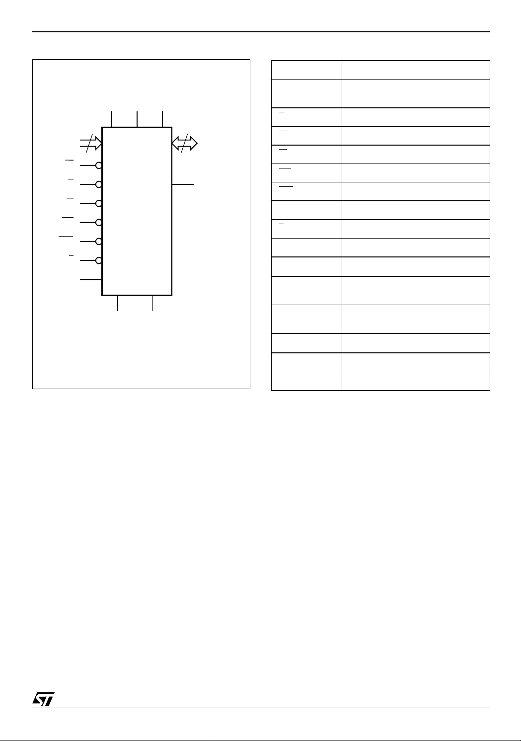
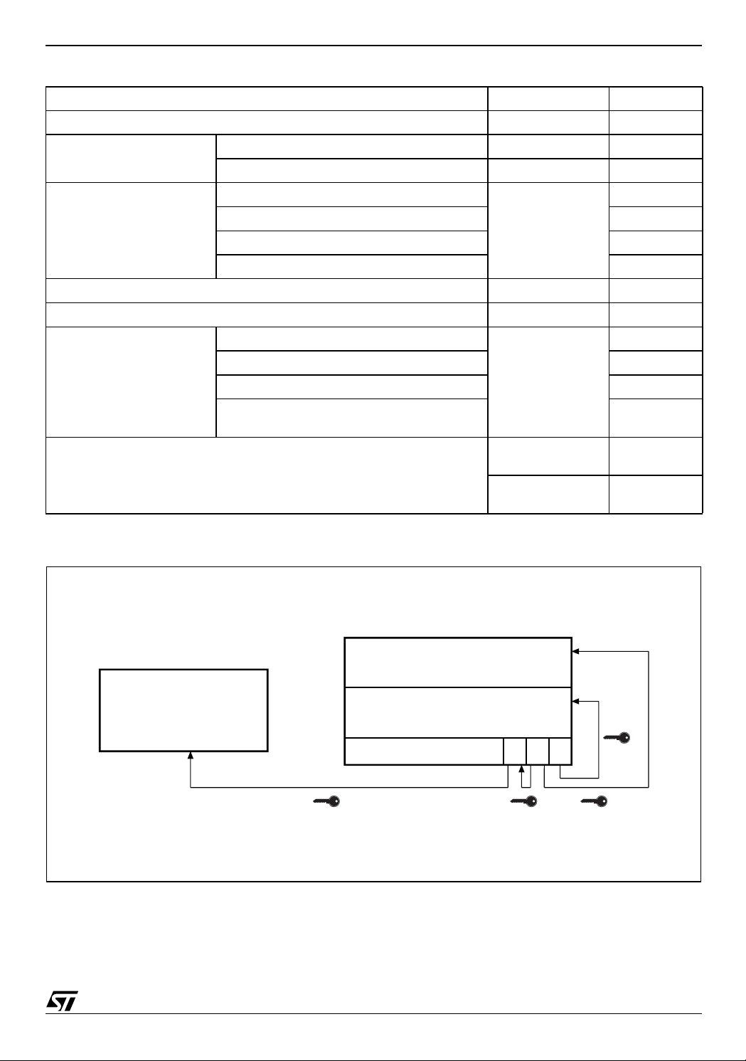
Figure 2. Logic Diagram Table 1. Signal Names
A0-A21 Address Inputs
A0-A21
W
RP
WP
Data Input/Outputs, Command
Inputs
Chip Enable
Output Enable
22
V
DD
V
DDQVPP
16
DQ0-DQ15
E
G
DQ0-DQ15
W
RP
E
G
M58WR064ET
M58WR064EB
L
WAIT
WP
KClock
L
WAIT Wait
V
DD
K
V
DDQ
SS
V
SSQ
AI05587
V
V
V
PP
SS
SSQ
V
Write Enable
Reset
Write Protect
Latch Enable
Supply Voltage
Supply Voltage for Input/Output
Buffers
Optional Supply Voltage for
Fast Program & Erase
Ground
Ground Input/Output Supply
NC Not Connected Internally
7/82
M58WR064ET, M58WR064EB
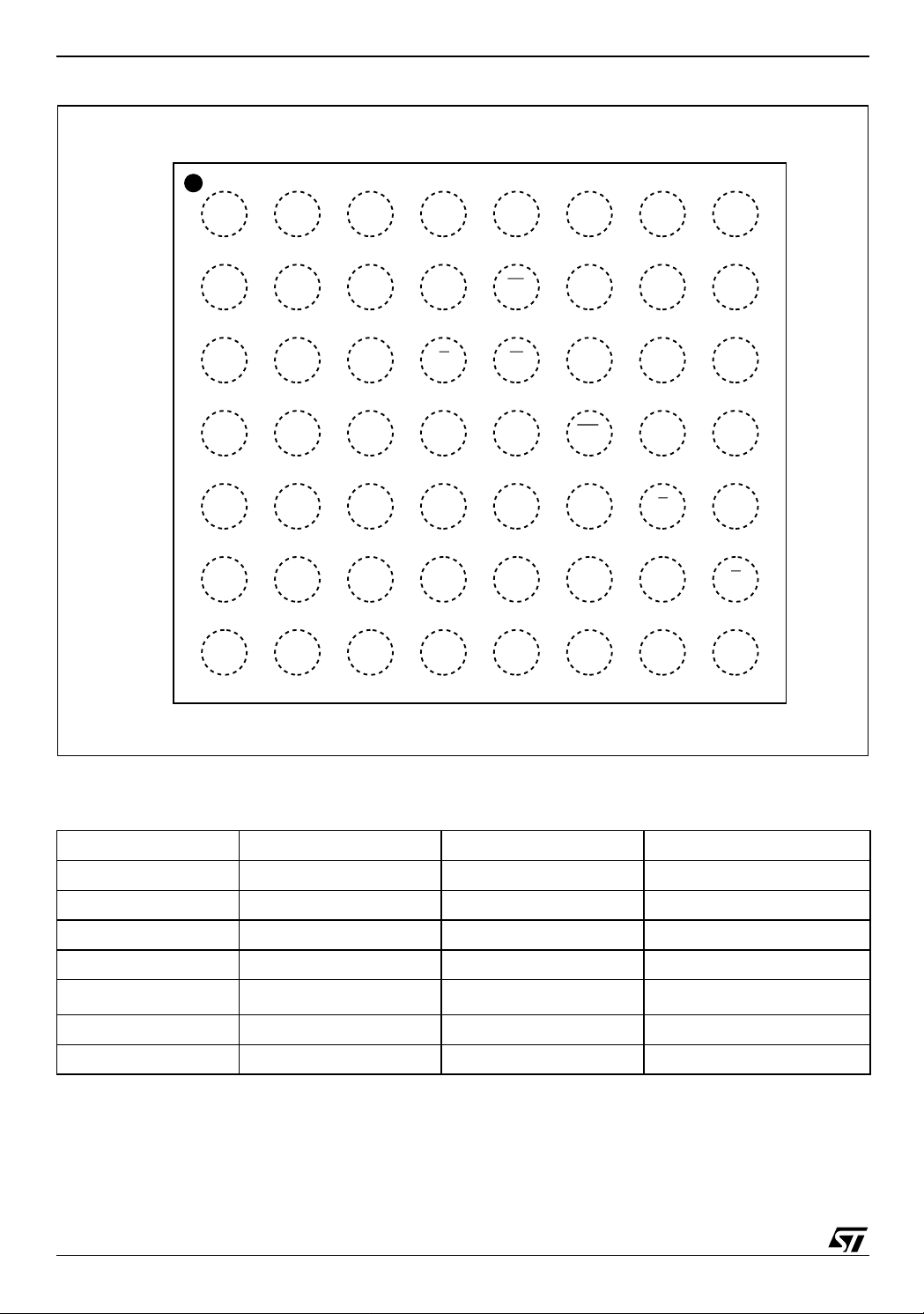
Figure 3. VFBGA Connections (To p view thro ugh packa ge)
87654321
A
B
C A2
D A1
E
F
G
A13
A15
V
DDQ
V
SS
DQ7 V
A8A11
A9A12
A10
A14 WAIT A16 WP
DQ15
DQ14 DQ11 DQ10 DQ9 DQ0 G
SSQ
V
SS
A20
A21
DQ6
DQ13
DQ5 V
V
DD
K RP
L W
DQ4 DQ2 E A0
DD
V
PP
DQ12
DQ3
A18
DQ1
V
DDQ
A6
A5A17
A7A19
NC
DQ8
V
A4
A3
SSQ
Table 2. Bank Architecture
Number Bank Size Parameter Blocks Main Blocks
Parameter Bank 4 Mbits 8 blocks of 4 KWords 7 blocks of 32 KWords
Bank 1 4 Mbits - 8 blocks of 32 KWords
Bank 2 4 Mbits - 8 blocks of 32 KWords
Bank 3 4 Mbits - 8 blocks of 32 KWords
----
Bank 14 4 Mbits - 8 blocks of 32 KWords
Bank 15 4 Mbits - 8 blocks of 32 KWords
8/82
----
----
AI06189
----
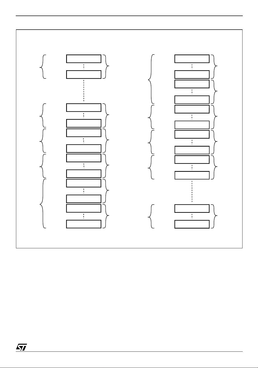
Figure 4. Me m ory Map
M58WR064ET, M58WR064EB
Bank 15
Bank 3
Bank 2
Bank 1
Parameter
Bank
M58WR064ET - Top Boot Block
Address lines A21-A0
000000h
007FFFh
038000h
03FFFFh
300000h
307FFFh
338000h
33FFFFh
340000h
347FFFh
378000h
37FFFFh
380000h
387FFFh
3B8000h
3BFFFFh
3C0000h
3C7FFFh
3F0000h
3F7FFFh
3F8000h
3F8FFFh
3FF000h
3FFFFFh
32 KWord
32 KWord
32 KWord
32 KWord
32 KWord
32 KWord
32 KWord
32 KWord
32 KWord
32 KWord
4 KWord
4 KWord
8 Main
Blocks
8 Main
Blocks
8 Main
Blocks
8 Main
Blocks
7 Main
Blocks
8 Parameter
Blocks
Parameter
Bank
Bank 1
Bank 2
Bank 3
Bank 15
M58WR064EB - Bottom Boot Block
Address lines A21-A0
000000h
000FFFh
007000h
007FFFh
008000h
00FFFFh
038000h
03FFFFh
040000h
047FFFh
078000h
07FFFFh
080000h
087FFFh
0B8000h
0BFFFFh
0C0000h
0C7FFFh
0F8000h
0FFFFFh
3C0000h
3C7FFFh
3F8000h
3FFFFFh
4 KWord
4KWord
32 KWord
32 KWord
32 KWord
32 KWord
32 KWord
32 KWord
32 KWord
32 KWord
32 KWord
32 KWord
8 Parameter
Blocks
7 Main
Blocks
8 Main
Blocks
8 Main
Blocks
8 Main
Blocks
8 Main
Blocks
AI06971b
9/82

M58WR064ET, M58WR064EB
SIGNAL DESCRIPTIONS
See Figure 2 Logic Diagram and Table 1,Signal
Names, for a brief overview of the signals connected to this device.
Address Inputs (A0-A21). The Address Inputs select the cells i n the memory array to a ccess during Bus Read operations. During Bus Write operations they control the commands sent to the Command Interface of the internal state machine.
Data Input/Output (DQ0-DQ15). The Data I/O outputs the data stored at the selected address during a Bus Read operation or inputs a command or the data to be programmed during a Bus Write operation.
Chip Enable (E
vates the memory control logic, input buffers, decoders and sense amplifiers. When Chip Enable is
and Reset is at VIH the device is in active
at V
IL
mode. When Chi p E nable i s at V
deselected, the outputs are high impedan ce and
the power consumption is reduced to the stand-by
level.
Output Enable (G
data outputs during the Bus Read operation of the
memory.
Write Enable (W
Bus Write operation of the memory’s Command
Interface. The data and address inputs are latched
on the rising edge of Chip Enable or Write Enable
whichever occurs first.
Write Protect (WP
that gives an additional hardware protection for
each block. When Write Protect is at V
Down is enabled and the prote ction status of t he
Locked-Down blocks cannot be changed. When
Write Protect is at V
and the Locked-Down blocks can be locked or unlocked. (refer to Table 13, Lock Status).
Reset (RP
ware reset of the memory. W hen Reset is at V
the memory is in reset mode: the outputs are high
impedance and the current consumption is reduced to the Reset Supply Current I
Table 2, DC Characteristics - Currents for the value of I
DD2.
state and the Configuration Register is reset.
When Reset is at V
eration. Exiting reset mode the device enters
asynchronous read mod e, but a negative transition of Chip Enable or Lat ch E nable is required to
ensure valid data outputs.
The Reset pin can be interfaced with 3V logic without any additional circuitry . It can be tied to V
(refer to Table 19, DC Characteristics).
Latch Enable (L
dress bits on its rising edge. The address
latch is transparent when Latch Enable is at
). The Chip Enable input acti-
the memory is
IH
). The Output Enable controls
). The Write Enable controls the
). Write Protect is an input
, the Loc k-
IL
, the Lock-Down is disabled
IH
). The Reset input provides a hard-
IL
. Refer to
DD2
After Reset all blocks are in the Locked
, the device is in normal op-
IH
RPH
). Latch Enable l atches the ad -
V
and it is inhibited whe n Latch Enable is at
IL
V
. Latch Enable can be kept Low (also at
IH
board level) when t he Latch Enable func tion
is not required o r sup ported.
Clo c k (K). The clock input synchronizes the memory to the microcontroller during synchronous read operations; the address is latched on a Clock edge (rising or falling, according to the configuration settings) when Latch Enable is at V don't care during asynchronous read and in write operations.
Wait (WAIT). Wai t is an output signal used during synchronous read to indicate whether the dat a on the output bus are valid. This output is high impedance when Chip Enable is at V
or Reset is at VIL.
IH
It can be configured to be active during the wait cycle or one clock cycle in advance. The WAIT signal
is not gated by Output Enable.
Supply Voltage . VDD provides the power
V
DD
supply to the internal core of the memory device.
It is the main power supply for all operations
(Read, Program and Erase).
Supply Voltage. V
V
DDQ
provides the power
DDQ
supply to the I/O pins and enables all Outputs to
be powered independently from V
tied to V
Program Supply Vol t age . VPP is both a
V
PP
or can use a separate supply.
DD
DD
. V
control input and a power supply pin. The two
functions are selected by the voltage range applied to the pin.
is kept in a low voltage range (0V to V
If V
PP
V
is seen as a control input. In this case a volt-
PP
age lower than V
against program or erase, whi le V
gives an absolute protection
PPLK
PP
ables these functions (see Tables 18 and 19, DC
Characteristics for the relevant values). V
sampled at the beginning of a program or erase; a
change in its value after the operation has started
does not have any effect and program or erase op-
,
erations continue.
is in the rang e of V
If V
PP
supply pin. In this condition V
it acts as a power
PPH
must be stable un-
PP
til the Program/Erase algorithm is completed.
V
Ground. VSS ground is the reference for t he
SS
core supply. It must be connected to the system
ground.
V
SSQ
Ground. V
ground is the reference for
SSQ
the input/output circuitry driven by V
must be connected to V
SS
Note: Each device in a system should have
V
DD, VDDQ
and VPP decoupled wi th a 0.1 µF ce-
ramic capacitor close to the pin (high frequency, inherently low inductance capacitors
should be as close as possible to the pack-
. Clock is
IL
DDQ
> V
PP
DDQ
can be
DDQ
en-
PP1
is only
. V
SSQ
)
10/82
M58WR064ET, M58WR064EB
age). See Figure 9, AC Measurement Load Circuit. The PCB trace widths should be sufficient
BUS OPERATIONS
There are six standard bus operations that control
the device. These are Bus Read , Bus Write, Address Latch, Output Disable, Standby and Reset.
See Table 3, Bus Operations, for a summary.
Typically glitches of less than 5ns on Chip Enable
or Write Enable are ignored by the memory and do
not affect Bus Write operations.
Bus Read. Bus Read operations are used to output the contents of the Memory Array, the Electronic Signature, the Status Register and the Common Flash Interface. Both Chip Enable and Output Enable must be at V
in order to perform a
IL
read operation. The Chip Enable input s hould be
used to enable the device. Out put Enable should
be used to gate data onto the output. The data
read depends on the previous command written to
the memory (see Command Interface section).
See Figures 10, 1 1, 12 and 13 Read AC Waveforms, and Tables 20 and 21 Read AC Characteristics, for details of when the output becomes
valid.
Bus Write. Bus Write operations write Commands to the memory or latch Input Data to be programmed. A bus write operation is initiated when Chip Enable and Write Enable are at V Output Enable at V
. Commands, Input Data and
IH
IL
with
Addresses are latched on the rising edge of Write
Enable or Chip Enable, whichever occurs first. The
addresses can also be latched prior to the write
operation by toggling Latc h Enable. In this case
to carry the re quired VPP program and erase
currents.
the Latch Enable shoul d be t ied to V
during the
IH
bus write operation.
See Figures 15 and 16, Write AC Waveforms, and
Tables 22 and 23, Write AC Characteristics, for
details of the timing requirements.
Address Latch. Address latch operations input valid addresses. Both Chip enable and Latch Enable must be at V
during address latch opera-
IL
tions. The addresses are latched on the rising
edge of Latch Enable.
Output Disa bl e . The outputs are high impedance when the Output Enable is at V
.
IH
Standby. Standby di sables most of the internal circuitry allowing a substantial reduction of the current consumption. The memory is in stand-by when Chip Enable and Reset are at V
. The pow-
IH
er consumption is reduced to the stand-by level
and the outputs are s et to high impedan ce, independently from the Output Enable or Write Enable
inputs. If Chip Enable switches to V
during a pro-
IH
gram or erase operation, the device enters Standby mode when finished.
Reset. During Reset mode the memory is deselected and the outputs are high impedance. The memory is in Reset mode when Reset is at V
IL
The power consumption is reduced to the Standby
level, independently from the Chip Enable, Output
Enable or Write Enable inputs. If Reset is pulled to
V
during a Program or Erase, this operation is
SS
aborted and the memory content is no longer valid.
.
Table 3. Bus Operations
Operation E G W L RP
Bus Read
Bus Write
Address Latch
Output Disable
Standby
Reset X X X X
Note: 1. X = Don’t care.
2. L
can be tied to VIH if the valid address has been previo usly latched.
3. Depends on G
4. WAIT signal pol arity is conf i gured usi ng t he Set Confi guration Regi ster comm and.
V
IL
V
IL
V
IL
V
IL
V
IH
.
V
IL
V
IH
X
V
IH
XXX
V
IH
V
IL
V
IH
V
IH
(2)
V
IL
(2)
V
IL
V
IL
X
WAIT
V
IH
V
IH
V
IH
V
IH
V
IH
V
IL
(4)
Hi-Z Hi-Z
Hi-Z Hi-Z
DQ15-DQ0
Data Output
Data Input
Data Output or Hi-Z
Hi-Z
(3)
11/82

M58WR064ET, M58WR064EB
COMMAND INTERFACE
All Bus Write operations t o the me mory are in terpreted by the Command Interface. Commands
consist of one or more sequential Bus Write operations. An internal Program/Erase Controller handles all timings and verifies the correct execution
of the Program and Erase commands. The Program/Erase Controller provides a S tatus Register
whose output may be read at any ti me to monitor
the progress or the result of the operation.
The Command Interface is reset to read mode
when power is first applied, when exiting from Reset or whenever V
is lower than V
DD
mand sequences must be followed exactly. Any
invalid combination of commands will be ignored.
Refer to Table 4, Command Codes and Appendix
D, Tables 40, 41, 42 and 43, Command I nterface
States - Modify and Lock Tables, for a summary of
the Command Interface.
The Command Interface is split into two type s of
commands: Standard commands and Factory
Program commands. The following sections explain in detail how to perform each command.
LKO
. Com-
Table 4. Command C odes
Hex Code Command
01h Block Lock Confirm
03h Set Configuration Register Confirm
10h Alternative Program Setup
20h Block Erase Setup
2Fh Block Lock-Down Confirm
30h Enhanced Factory Program Setup
35h Double Word Program Setup
40h Program Setup
50h Clear Status Register
56h Quadruple Word Program Setup
60h
70h Read Status Register
75h
80h Bank Erase Setup
Block Lock Setup, Block Unlock Setup,
Block Lock Down Setup and Set
Configuration Register Setup
Quadruple Enhanced Factory Program
Setup
90h Read Electronic Signature
98h Read CFI Query
B0h Program/Erase Suspend
C0h Protection Register Program
Program/Erase Resume, Block Erase
D0h
FFh Read Array
Confirm, Bank Erase Confirm, Block
Unlock Confirm or Enhanced Factory
Program Confirm
12/82

COMMAND INTERFACE - STANDARD COMMANDS
The following commands are the basic commands
used to read, write to and configure the device.
Refer to Table 5, Standard Commands, in conjunction with the following text descriptions.
Read Array Command
The Read Array comm and returns the addressed
bank to Read Array mode. One Bus Write cycle is
required to issue the Read Array command and return the addressed bank to Read Array mode.
Subsequent read operations will read the addressed location and output t he data. A Read Array command can be issued in one bank while
programming or erasing in another bank. However
if a Read Array command is issued to a bank currently executing a Program or Erase operation the
command will be e xecuted but t he output da ta is
not guaranteed.
Read Status Register Command
The Status Register indi cates when a Program or
Erase operation is complete and the success or
failure of operation itself. Issue a Read Status
Register command to read the Status Register
content. The Read Status Register com man d c an
be issued at any time, even during Program or
Erase operations.
The following read operations output the content
of the Status Register of the addressed bank. The
Status Register is latched on the falling edge of E
or G signals, and can be read until E or G returns
. Either E or G must be toggled to update the
to V
IH
latched data. See Table 8 for the description of the
Status Register Bits. This mode supports asynchronous or single synchronous reads only.
Read Electronic Signature Command
The Read Electronic Signature command reads
the Manufacturer and Device Codes, the Block
Locking Status, the Protection Register, and the
Configuration Register.
The Read Electronic Signature command consists
of one write cycle to an address within one o f the
banks. A subsequent Read ope ra tion in the same
bank will output the Manufacturer Code, the Device Code, the protection Status of the blocks in
the targeted bank, the Protection Register, or the
Configuration Register (see Table 6).
If a Read Electronic Signature command is issued
in a bank that is executing a Program or Erase operation the bank will go into Read Electronic Signature mode, subsequent Bus Read cycles will
output the Electronic Sign ature data an d the Pr ogram/Erase controller will continue t o program or
erase in the background. This mode supports
asynchronous or single synchronous reads only, it
does not support page mode or synchronous burst
reads.
M58WR064ET, M58WR064EB
Read CFI Query Command
The Read CFI Query command is used to read
data from the Common Flash Interface (CFI). The
Read CFI Query Command consists of one Bus
Write cycle, to an address within one of the banks.
Once the command is issued subsequent Bus
Read operations in the s ame bank read from the
Common Flash Interface.
If a Read CFI Query command is issued in a bank
that is executing a Program or Erase operation the
bank will go into Read CFI Query mo de, subsequent Bus Read cycles will output the CFI data
and the Program/Erase con troller will continue to
Program or Erase in the background. This m ode
supports asynchronous or single synchronous
reads only, it does not support page mode or synchronous burst reads.
The status of the other banks is not affected by the
command (see Table 11). After issuing a Read
CFI Query command, a Read Array command
should be issued to t he address ed bank to return
the bank to Read Array mode.
See Appendix C, Common Flash Interface, Tables
30, 31, 32, 33, 34, 36, 37, 38 and 39 for details on
the information contained in the Common Flash Interface memory area.
Clear Status Register Command
The Clear Status Register comm and c an b e us ed
to reset (set to ‘0’) error bits 1, 3, 4 and 5 in the Status Register. One bus write cycle is required to issue the Clear Status Register command. The
Clear Status Register com man d do es not c ha nge
the Read mode of the bank.
The error bits in the Status Regi ster do not automatically return to ‘0’ when a new command is issued. The error bits i n the Stat us Register should
be cleared before attempting a new Program or
Erase command.
Block Erase Command
The Block Erase com mand can be used to erase
a block. It sets all the bits within the selected block
to ’1’. All previous d ata in th e block is lost. If th e
block is protected then the Erase operation will
abort, the data in the block will not be changed and
the Status Register will output the error. The Block
Erase command can be issued at any moment, regardless of whether the block has been programmed or not.
Two Bus Write cycles are required to issue the
command.
■ The first bus cycle sets up the Erase command.
■ The second latches the block address in the
internal state machine and starts the Program/
Erase Controller.
13/82

M58WR064ET, M58WR064EB
If the second bus cycle is not Write Erase Confirm
(D0h), Status Register bits 4 and 5 are set and the
command aborts. Erase aborts if Reset turns to
. As data integrity cannot be guaranteed when
V
IL
the Erase operation is aborted, the block must be
erased again.
Once the command is issued the device outputs
the Status Register data when any address within
the bank is read. At the end o f the operation the
bank will remain in Read Status Register mode until a Read A rray, Read CFI Query o r Read Electronic Signature command is issued.
During Erase operations the bank containing the
block being erased will only accept the Read Array, Read Status Register, Read Electronic Signature, Read CFI Query and the Program/Erase
Suspend command, all other commands will be ignored. Refer to Dual Operations section for detailed information about simultaneous operations
allowed in banks not being e rased. Typical Erase
times are given in Table 14, Program, Erase
Times and Program/Erase Endurance Cycles.
See Appendix C, Figure 25, Block Erase Flowchart and Pseudo Code, for a suggested flowchart
for using the Block Erase command.
Program Command
The memory array can be programmed word-byword. Only one Word in one bank can be programmed at any one time. Two bus write cycles
are required to issue the Program Command.
■ The first bus cycle sets up the Program
command.
■ The second latches the Address and the Data to
be written and starts the Program/Erase
Controller.
After programming has started, read operations in
the bank being programmed output the Status
Register content.
During Program operations the bank being programmed will only accept the Read Array, Read
Status Register, Read Electronic Signature, Read
CFI Query and the Program/Erase Suspend command. Refer to Dual Operations section for detailed information about simultaneous operations
allowed in banks not bei ng programmed. Typical
Program times are given in Table 14, Program,
Erase Times and Program/Erase Endurance Cycles .
Programming aborts if Reset goe s to V
. As data
IL
integrity cannot be guaranteed when the program
operation is aborted, the memory location must be
reprogrammed.
See Appendix C, Figure 21, Program Flowchart
and Pseudo Code, for the f lowchart for using the
Program command.
Program/Erase Suspend Command
The Program/Erase Suspend command is used to
pause a Program or Block Erase operation. A
Bank Erase operation cannot be suspended.
One bus write cycle is required to issue t he Program/Erase command. O nce the Program/Erase
Controller has paused bits SR7, SR6 and/ or SR2
of the Statu s Regist er will be s et to ‘1’. Th e command can be addressed to any bank.
During Program/Erase Suspend the Command Interface will accept the Program/Erase Resume,
Read Array (cannot read the erase-suspended
block or the program-suspended Word), Read
Status Register, Read Electronic Signature and
Read CFI Query commands. Additionally, if the
suspend operation was E rase then the Clear status Register, Program, Block Lock, Block LockDown or Block Unlock commands will also be accepted. The block being erased may be protected
by issuing the Block Lock, Block Lock-Down or
Protection Register Program commands. Only the
blocks not being erased may be read or programmed correctly. When the Program/Erase Resume command is issued the operation will
complete. Refer to the Dual Operations section for
detailed information about simultaneous operations allowed during Program/Erase Suspend.
During a Program/Erase Suspend, the device can
be placed in standby mode by taking Chip Enable
. Program/Erase is aborted if Reset turns to
to V
IH
V
.
IL
See Appendix C, Figure 24 , Program Suspend &
Resume Flowchart and Pseudo Code, and Figure
26, Erase Suspend & Resume Flowchart and
Pseudo Code for flowcharts for using the Program/
Erase Suspend command.
Program/Erase Resu me Command
The Program/Erase Resume command can be
used to restart the Program/Erase Controller after
a Program/Erase Suspen d command has paused
it. One Bus Write cycle is required to issue the
command. The command can be written to any
address.
The Program/Erase R esume command d oes not
change the read m ode of the banks. If the s uspended bank was in Read Status Register, Read
Electronic signature or Read CFI Query mode the
bank remains in that m ode and outputs the corresponding data. If the bank was in Read Array
mode subsequent read operations will output invalid data.
If a Program command is issued during a Block
Erase Suspend, then the erase cannot be resumed until the programming operation has completed. It is possible to accumulate suspend
operations. For example: su spend an erase operation, start a programming operation, suspend the
14/82

M58WR064ET, M58WR064EB
programming operation then read the array. See
Appendix C, Figure 24, Program Su spend & Resume Flowchart and Pseudo Code, and Figure 26,
Erase Suspend & Resume Flowchart and Pseudo
Code for flowcharts for using the Program/Erase
Resume command.
Protectio n R egist er Progr am C om m and
The Protection Register Program command is
used to Program the 128 bit user O ne-Time-Programmable (OTP) segment of the Protection Register and the Protection Register Lock. The
segment is programmed 16 bits at a time. When
shipped all bits in the segment are set to ‘1’. The
user can only program the bits to ‘0’.
Two write cycles are required to issue the Protection Register Program command.
■ The first bus cycle sets up the Protection
Register Program command.
■ The second latches the Address and the Data to
be written to the Protection Register and starts
the Program/Erase Controller.
Read operations output the Status Register content after the programming has started.
The segment can be protected by programming bit
1 of the Protection Lock Register. Bit 1 of the Protection Lock Register also protects bit 2 of the Protection Lock Register. Programming bit 2 of the
Protection Lock Register will result in a permanent
protection of Parameter Block #0 (see Figure 5,
Security Block and Protection Register Memory
Map). Attempting to program a previously protected Protection Register will result in a Status Register error. The protection of the Protection
Register and/or the Security Block is not reversible.
The Protection Register Program cannot be suspended. See Appendix C, Figure 28, Protection
Register Program Flowchart and Pseudo Code,
for a flowchart for using the Protection Register
Program command.
Set Conf ig uration Regi s te r C om m and
The Set Configuration Register command is used
to write a new value to the Burst Configuration
Control Register which defines the burst length,
type, X latency, Synchronous/Asynchronous Read
mode and the valid Clock edge configuration.
Two Bus Writ e cycles a re required to i ssue the Set
Configuration Register command.
■ The first cycle writes the setup command and
the address corresponding to the Configuration
Register content.
■ The second cycle writes the Configuration
Register data and the confirm command.
The Read mode of the banks is not modified when
the Set Configuration Register command is issued.
The value for the Configuration Register is always
presented on A0-A15. CR0 is on A0, CR1 on A1,
etc.; the other address bits are ignored.
Block Lock Command
The Block Lock command is used to lock a block
and prevent Program or Erase operations from
changing the data in it. All blocks are locked at
power-up or reset.
Two Bus Write cycles are required to issue the
Block Lock command.
■ The first bus cycle sets up the Block Lock
command.
■ The second Bus Write cycle latc hes the block
address.
The lock status can be monitored for each block
using the Read Electronic Signature command.
Table. 13 shows the Lock Status after issuing a
Block Lock command.
The Block Lock bits are vo latile, once set they remain set until a hardware reset or power-down/
power-up. They are cleared by a Block Unlock
command. Refer to the section, Block Locking, for
a detailed explanation. See Appendix C, Figure
27, Locking Operations Flowchart and Pseudo
Code, for a flowchart for using the Lock command.
Block Unlock Command
The Block Unlock command is used to unlock a
block, allowing the block to be programmed or
erased. Two Bus Write cycles are requ ired to issue the Block Unlock command.
■ The first bus cycle sets up the Block Unlock
command.
■ The second Bus Write cycle latc hes the block
address.
The lock status can be monitored for each block
using the Read Electronic Signature command.
Table 13 shows the protection status after issuing
a Block Unlock command. Refer to the section,
Block Locking, for a detailed expla nation and A ppendix C, Figure 27, Locking Operations Flowchart and Pseudo Code, f or a flowchart for using
the Unlock command.
Block Lock-Down Command
A locked or unlocked block can be locked-down by
issuing the Block Lock-Down command. A lockeddown block cannot be programm ed or erased, or
have its protection status changed when WP
low, V
. When WP is high, V
IL
the Lock-Down
IH,
is
function is disabled and the locked blocks can be
individually unlocked by the Block Unlock command.
Two Bus Write cycles are required to issue the
Block Lock-Down command.
■ The first bus cycle sets up the Block Lock
command.
15/82

M58WR064ET, M58WR064EB
■ The second Bus Write cycle latches the blo ck
address.
The lock status can be monitored for each block
using the Read Electronic Signature command.
Locked-Down blocks revert to the locked (and not
locked-down) state when the device is reset on
power-down. Table. 13 shows the Lo ck Statu s after issuing a Block Lock-Down command. Refer to
the section, Block Locking, for a detailed explanation and Appendix C, Fi gure 27, Locking Operations Flowchart and Pseudo Code, for a flowchart
for using the Lock-Down command.
Table 5. Standard Commands
Bus Operations
Commands
Cycles
Op. Add Data Op. Add Data
Read Arra y 1+ Write BKA FFh
Read Status Register 1+ Write BKA 70h Read
Read Electro nic Signature 1+ Write BKA 90h Read
Read CFI Query 1+ Write BKA 98h Read
Clear Status Register 1 Write BKA 50h
Block Erase 2 Wri t e
Program 2 Write
Program/E rase Su s pen d 1 Write X B0h
Program/Erase Resume 1 Write X D0h
Protection Register Program 2 Write PRA C0h Write
Set Configuration Register 2 Write CRD 60h Write
Block Loc k 2 Write
Block Unlock 2 Wri te
Block Loc k-Down 2 Write
Note: 1. X = Don’t Care, WA=Word Address in targeted bank, RD=Read Data, SRD=Status Register Data, ESD=Electronic Signature Data,
QD=Query Dat a, BA=Bl ock Address, BK A= Ban k Address , PD= Program Data, PR A=Prot ectio n Regist er Addre ss, PRD =Prote ction
Register Dat a, CRD=Configuration Regis ter Data.
2. Must be same bank as in the first cycle. The signature address es are listed i n T able 6.
3. Any address within the bank can be used.
1st Cycle 2nd Cycle
BKA or BA
BKA or WA
Read
(3)
(3)
20h Write BA D0h
40h or 10h Write WA PD
WA RD
BKA
BKA
BKA
PRA PRD
CRD
BKA or BA
BKA or BA
BKA or BA
(3)
(3)
(3)
60h Write BA 01h
60h Write BA D0h
60h Write
BA
(2)
(2)
(2)
SRD
ESD
QD
03h
2Fh
16/82
M58WR064ET, M58WR064EB
Table 6. Electronic Signature Codes
Code Address (h) Dat a (h)
Manufacturer Code Bank Address + 00 0020
Device Code
Top Bank Address + 01 8810
Bottom Bank Address + 01 8811
Lock
0001
Unlocked 0000
Block Protection
Block Address + 02
Locked and Locked-Down 0003
Unlocked and Locked-Down 0002
Reserved Bank Address + 03 Reserved
Configuration Register Bank Address + 05 CR
ST Factory Default
0006
Security Block Permanently Locked 0002
Protection Register Lock
OTP Area Permanently Locked 0004
Security Block and OTP Area Permanently
Locked
Bank Address + 80
Bank Address + 81
Bank Address + 84
0000
Unique Device
Number
Protection Register
Bank Address + 85
Bank Address + 8C
Note: CR=Con figurati on Register.
OTP Area
Figure 5. Security Block and Protection Register Memory Map
SECURITY BLOCK
Parameter Block # 0
8Ch
85h
84h
81h
80h
PROTECTION REGISTER
User Programmable OTP
Unique device number
Protection Register Lock 2 1 0
AI06181
17/82

M58WR064ET, M58WR064EB
COMMAND INTERFACE - FACTORY PROGRAM COMMANDS
The Factory Program commands are used to
speed up programming. They require V
V
except for the Bank Eras e command which
PPH
also operates at V
= VDD. Refer to Table 7, Fac-
PP
to be at
PP
tory Program Commands, in conjunction with the
following text descriptions.
The use of Factory Program comma nds requires
certain operating conditions.
■ V
must be set t o V
PP
(except for Bank Erase
PPH
command),
■ V
must be within operating range,
DD
■ Ambient temperature, T
■ The targeted block must be unlocked.
must be 25°C ± 5°C,
A
Bank Erase Command
The Bank Erase command can be used to erase a
bank. It sets all the bits within the selected bank to
’1’. All previous data in th e ban k is lo st. Th e B ank
Erase command will igno re any protected blocks
within the bank. If all blocks in the ba nk are protected then the Bank Erase operation will abort
and the data in the bank wi ll not b e changed. The
Status Register will not output any error.
Bank Erase operations can be p erformed at both
= V
V
PP
and VPP = VDD.
PPH
Two Bus Write cycles are required to issue the
command.
■ The first bus cycle sets up the Bank Erase
command.
■ The second latches the bank address in the
internal state machine and starts the Program/
Erase Controller.
If the second bus cycle is not Write Bank Erase
Confirm (D0h), Status Register bits SR4 and S R5
are set and the command aborts. Erase aborts if
Reset turns to V
. As data integrity cannot be
IL
guaranteed when the Erase operation is aborted,
the bank must be erased again.
Once the command is issued the device outputs
the Status Register data when any address within
the bank is read. At the end o f the operation the
bank will remain in Read Status Register mode until a Read Array, Read CFI Query or Read Electronic Signature command is issued.
During Bank Erase operations the bank being
erased will only accept the Read Array, Read Status Register, Read Electronic Signature and Read
CFI Query command, all other commands will be
ignored.
For optimum performance, Bank Erase commands should be limited to a maximum of 100 Program/Erase cycles per Block. After 100 Program/
Erase cycles the internal algorithm will still operate
properly but some degradation in performance
may occur.
Dual operations are not supported during Bank
Erase operations and the command cannot be
suspended.
Typical Erase times are given in Table 14, Program, Erase Times and Program/Erase Endurance Cycles.
Double Word Program Command
The Double Word Program command improves
the programming throughput by writing a page of
two adjacent words in parallel. The two words
must differ only for the address A0.
Three bus write cycles are neces sary to issue the
Double Word Program command.
■ The first bus cycle sets up the Double Word
Program Command.
■ The second bus cycle latches the Address and
the Data of the first word to be written.
■ The third bus cycle latches the Address and the
Data of the second word to be written and starts
the Program/Erase Controller.
Read operations in the bank bei ng programmed
output the Status Register content after the programming has started.
During Double Word Program operations the bank
being programmed will only accept the Read Array, Read Status Register, Read Electronic Signature and Read CFI Query command, all other
commands will be ignored. Dual operations are
not supported during Double Word Program operations and the command cannot be suspended.
Typical Program times are given in Table 14, Program, Erase Times and Program/Erase Endurance Cycles.
Programming aborts if Reset goe s to V
integrity cannot be guaranteed when the program
operation is aborted, the memory locations m ust
be reprogrammed.
See Appendix C, Figure 22, Double Word Program Flowchart and Pseudo Code, for the flowchart for using the Double Word Program
command.
Quadruple Word Program Command
The Quadruple Word Program command improves the programming throughput by writing a
page of four adjacent words in parallel. The four
words must differ only for the addresses A0 and
A1.
Five bus write cycles are necessary to issue the
Quadruple Word Program command.
■ The first bus cycle sets up the Double Word
Program Command.
■ The second bus cycle latches the Address and
the Data of the first word to be written.
. As data
IL
18/82

M58WR064ET, M58WR064EB
■ The third bus cycle latches the Address and the
Data of the second word to be written.
■ The fourth bus cycle latches the Address and
the Data of the third word to be written.
■ The fifth bus cycl e latches the Addres s and th e
Data of the fourth word to be written and starts
the Program/Erase Controller.
Read operations to the bank being programmed
output the Status Register content after the programming has started.
Programming aborts if Reset goe s to V
. As data
IL
integrity cannot be guaranteed when the program
operation is aborted, the memory locations mu st
be reprogrammed.
During Quadruple Word Program operations the
bank being programmed will only accept the Read
Array, Read Status Register, Read Electronic Signature and Read CFI Query command, all other
commands will be ignored.
Dual operations are not supported during Quadruple Word Program operations and the command
cannot be suspended. Typi cal Program times are
given in Table 14, Program, Erase Times and Program/Erase Endurance Cycles.
See Appendix C, Figure 23, Quadruple Word Program Flowchart and Pseudo Code, for the flowchart for using the Quadruple Word Program
command.
Enhanced Factory Program Command
The Enhanced Factory Program command can be
used to program large streams of dat a within any
one block. It greatly reduces the total programming time when a large number of Words are written to a block at any one time.
Dual operations are not s upported during the Enhanced Factory Program operation an d the command cannot be suspended.
For optimum performance the Enhanc ed Factory
Program commands should be limited to a maximum of 10 program/erase cycles per block. If this
limit is exceeded the in ternal algorithm will c ont inue to work properly but some degradation in performance is possible. Typical Prog ram times are
given in Table 14.
The Enhanced Factory Program command has
four phases: the Setup Phase, the Program Phase
to program the data to the memory, the Verify
Phase to check that the data has been correctly
programmed and reprogram if necessary a nd the
Exit Phase. Refer to Table 7, Enhanced Factory
Program Command and Figure 29, Enhanced
Factory Program Flowchart.
Setup Phase. The Enhanced Factory Program
command requires two Bus Write operations to initiate the command.
■ The first bus cycle sets up the Enhanced
Factory Program command.
■ The second bus cycle confirms the command.
The Status Register P/E.C. Bit 7 should be read to
check that the P/E.C. is ready. After the confirm
command is issued, read operations output the
Status Register data. The read Status Register
command must not be issued as it will be
interpreted as data to program.
Program Phase. The Program Phase requires
n+1 cycles, wher e n is the n umber of Words (refer
to Table 7, Enhanced Factory Program Command
and Figure 29, Enhanced Factory Program Flowchar t).
Three successive steps are required to issue and
execute the Program Phase of the command.
1. Us e one Bus Write operation to latch the Start
Address and the first Word to be programmed.
The Status Register Bank Write Status bit SR0
should be read to check that the P/E.C. is ready
for the next Word.
2. Each subsequent Word to be programmed is
latched with a new Bus Write operation. The
address can either remain the Start Address, in
which case the P/E.C. increments the address
location or the address can be incremented in
which case the P/E.C. jumps to the new
address. If any address that is not in the same
block as the Start Address is given with data
FFFFh, the Program Phase terminates and the
Verify Phase begins. The Status Register bit
SR0 should be read between each Bus Write
cycle to check that the P/E.C. is ready for the
next Word.
3. Finally, after all Words have been programmed,
write one Bus Write operation with data FFFF h
to any address outside the bl ock contain ing the
Start Address, to terminate the programming
phase. If the data is not FFFFh, the command is
ignored.
The memory is now set to enter the Verify Phase.
Verify Phase. Th e Verify Phase is s imilar to the
Program Phase in that all Words must be resent to
the memory for them to be che cked against the
programmed data. The Program/Erase Controller
checks the stream of da ta with the data that was
programmed in the Program Phase and reprograms the memory location if necessary.
Three successive steps are required to execute
the Verify Phase of the command.
1. Us e one Bus Write operation to latch the Start
Address and the first Word, to be verified. The
Status Register bit SR0 should be read to check
that the Program/Erase Controller is ready for
the next Word.
19/82

M58WR064ET, M58WR064EB
2. Each subsequent Word to be verified is latched
with a new Bus Write operation. The Words
must be written in the same order as in the
Program Phase. The address can remain the
Start Address or be incremented. If any address
that is not in the same block as the Start
Address is given with data FFFFh, the Verify
Phase terminates. Status Register bit SR0
should be read to check that the P/E.C. is ready
for the next Word.
3. Finally, after all Words have been verified, write
one Bus Write operation with data FFFFh to any
address outside the block containing the Start
Address, to terminate the Verify Phase.
If the Verify Phase is successfully completed the
memory remains in Read Status Register mode. If
the Program/Erase Controller fails to reprogram a
given location, the error will be signaled in the Status Register.
Exit Phase. Status Register P/E.C. bit SR7 set to
‘1’ indicates that the device has ret urned to Read
mode. A full Status Register check should be done
to ensure that the block has been successfully programmed. See the s ect ion on the Status Register
for more details.
Quadruple Enhanced Factory Program Command
The Quadruple Enhanced Factory Program command can be used to program one or more pages
of four adjacent Words in parallel. The four Words
must differ only for the addresses A0 and A1.
Dual operations are not supported during Quadruple Enhanced Factory Program operations and
the command cannot be suspended.
The Quadruple Enhanced Factory Program command has four phases: the Setup Phase, the Load
Phase where the data is loaded into the buffer, the
combined Program and Verify Phase where the
loaded data is programmed to the memory and
then automatically checked and reprogrammed if
necessary and the Exit Phase. Unlike the Enhanced Factory Program it is not necess ary t o resubmit the data for the Verify Phase. The Load
Phase and the Program and Verify Phas e can be
repeated to program any number of pag es within
the block.
Setup Phase. The Q uadruple Enhan ced Factory
Program command requires one Bus Write operation to initiate the load phase. After the setup
command is issued, read operations output the
Status Register data. The Read Status Register
command must not be issued as it will be
interpreted as data to program.
Load Phase. The Load Phase requires 4 cycles
to load the data (refer to Table 7, Factory Program
Commands and Figure 30, Quadruple Enhanced
Factory Program Flowchart). Once the first Word
of each Page is written it is impossible to exit the
Load phase until all four Words have been written.
Two successive steps are required to issue and
execute the Load Phase of the Quadruple Enhanced Factory Program comm and.
1. Us e one Bus Write operation to latch the Start
Address and the first Word of the first Page to
be programmed. For subsequent Pages the first
Word address can remain the Start Address (in
which case the next Page is programmed) or
can be any address in the same block. If any
address with data FFFFh is given that is not in
the same block as the Start Address, the device
enters the Exit Phase. For the first Load Phase
Status Register bit SR7 should be read after the
first Word has been issued to check that the
command has been accepted (bit SR7 set to
‘0’). This check is not required for subsequent
Load Phases.
2. Each subsequent Word to be programmed is
latched with a new Bus Write operation. The
address is only checked for the first Word of
each Page as the order of the Words to be
programmed is fixed.
The memory is now set to enter the Program and
Verify Phase.
Program and Verify Phase. In the Program and
Verify Phase the four Words that were loaded in
the Load Phase are programmed in the memory
array and then verified by the Program/Erase Controller. If any errors are found the Program/Erase
Controller reprograms the location. During this
phase the Status Register shows that the Program/Erase Controller is busy, Status Register bit
SR7 set to ‘0’, and that the device is not waiting for
new data, Status Register bit SR0 set to ‘1’. When
Status Register bit SR0 i s set to ‘0’ the Program
and Verify phase has terminated.
Once the Verify Phase has successfully completed subsequent pages in the same block can be
loaded and programmed. The device returns to
the beginning of the Load Phase by issuing one
Bus Write operation to latch the A ddress and the
first of the four new Words to be programmed.
Exit Phase. Finally, after all the pages have been
programmed, write one Bus Write operation with
data FFFFh to any address outside the block containing the Start Address, to terminate the Load
and Program and Verify Phases.
Status Register bit SR7 set t o ‘1’ a nd bit S R0 set
to ‘0’ indicate that the Quadruple Enhanced Factory Program command has terminated. A full Status
Register check should be done to ensure that the
block has been sucessfully programmed. See the
section on the Status Register for more details.
If the Program and Verify Phase has successfully
completed the memory returns to Read mode. If
20/82

the P/E.C. fails to program and reprogram a given
location, the error will be signaled in the Status
Register.
Table 7. Factory Program Commands
Command Phase
Bank Erase
Double Word Program
Cycles
2
(4)
3
1st 2nd 3rd Final -1 Final
Add Data Add Data Add Data Add Data Add Data
BKA 80h BKA D0h
BKA or
WA1
35h WA1 PD1 WA2 PD2
(8)
M58WR064ET, M58WR064EB
Bus Write Operations
Quadruple Word
Program
(5)
Enhanced
Factory
Program
Setup,
Program
(6)
Verify, Exit n+1
Setup,
first Load
5
2+
n+1
5
BKA or
(8)
WA1
BKA or
(8)
WA1
(2)
WA1
BKA or
(8)
WA1
56h WA1 PD1 W A2 PD2 WA3 PD3 WA4 PD4
30h
PD1
75h
BA or
WA1
WA2
WA1
(9)
(3)
(2)
D0h
PD2
PD1
WA1
WA3
WA2
(2)
(3)
(7)
PD1
PD3
PD2
WAn
WAn
WA3
(3)
(3)
(7)
PAn
PAn
PD3
NOT
WA1
NOT
WA1
WA4
First
Quadruple
Enhanced
Factory
Program
(5,6)
Program &
Verify
Subsequent
Loads
Subsequent
Program &
Automatic
WA1i
4
(2)
PD1i
WA2i
(7)
PD2i
WA3i
(7)
PD3i
Automatic
WA4i
(7)
Verify
NOT
Exit 1
Note: 1. WA=Word Add ress in t argeted bank, BKA= Bank A ddress, P D= P rogram Data, BA =Block Address .
2. WA1 is the Start Address. NOT WA1 is any addres s t hat i s not in the same bl ock as W A1.
3. Address ca n remain Starting Address WA1 or be i ncremented.
4. Word Addres ses 1 and 2 must be consecutive Addresses differing only for A0.
5. Word Addres ses 1,2,3 and 4 must be consecutive Addresses di ffering onl y for A0 and A1.
6. A Bus Read mus t b e d one bet ween eac h Wr ite cyc le where t he da t a is p rog ram med or v erif ied to read t he Stat us R eg ister an d
check that the memory is ready to accept the next dat a. n = number of Words, i = number of Pages to be progr am m ed.
7. Address is o nly che ck ed for the fir st Wo rd of ea ch Page a s the o rder t o pro gram the Wo rds i n each pag e is fixe d so su bs equent
Words in each Page can be written to any address.
8. Any address within the bank can be used.
9. Any addres s within the bl ock can be use d.
WA1
(2)
FFFFh
(2)
(2)
(7)
FFFFh
FFFFh
PD4
PD4i
21/82

M58WR064ET, M58WR064EB
STATUS REGISTER
The Status Register provides information on the
current or previous Program or Erase operations.
Issue a Read Status Register command to read
the contents of the Status Register, refer to Read
Status Register Command section for more details. To output the contents, the Status Register is
latched and updated on the falling edge of the
Chip Enable or Output Enable signal s and c an be
read until Chip Enable or Output Enable returns to
V
. The Status Register can only be read using
IH
single asynchronous or single synchronous reads.
Bus Read operations from any address within the
bank, always read the Status Register during Program and Erase operations.
The various bits convey information about the status and any errors of the operation. Bits SR7, SR6,
SR2 and SR0 give information on the status of the
device and are set and reset by the device. Bits
SR5, SR4, SR3 and S R1 give information on errors, they are set by the device but must be reset
by issuing a Clear Status Register command or a
hardware reset. If an error bit is set to ‘1’ the Status
Register should be reset before issuing another
command. SR7 to SR1 ref er to the status of the
device while SR0 refers to the status of the addressed bank.
The bits in the Status Register are summarized in
Table 8, Status Register Bits. Refer to Table 8 in
conjunction with the following text descriptions.
Program/Erase Controller Status Bit (SR7). The
Program/Erase Controller Status bit indicates
whether the Program/Erase Controller is act ive or
inactive in any bank. When the Program/Erase
Controller Status bit is Low (set to ‘0’), the Program/Erase Controller is active; when the bit is
High (set to ‘1’), the Program/Erase Controller is
inactive, and the device is ready to process a new
command.
The Program/Erase Controller Status is Low immediately after a Program/Erase Suspend command is issued until the Program/Erase Controller
pauses. After the Program/Erase Controller pauses the bit is High.
During Program, Erase, o perations the Program/
Erase Controller Status bit can be polled to find the
end of the operation. Other bits in the Status Register should not be tested until the Program/Erase
Controller completes the operation and the bit is
High.
After the Program/Erase Cont roller completes its
operation the Erase Status, Prog ram Status, V
Status and Block Lock Status bits should be tested
for errors.
Erase Suspend Status Bit (SR6). The Erase
Suspend Status bit indicates that an Erase operation has been suspended or is going to be sus-
PP
pended in the addressed block. When the Eras e
Suspend Status bit is High (set to ‘1’), a Program/
Erase Suspend command has been issued and
the memory is waiting for a Program/Erase Resume command.
The Erase Suspend Status should only be considered valid when the Program/Erase Controller Status bit is High (Program/Erase Controller inactive).
SR7 is set within the Erase Suspend Latency time
of the Program/Erase Suspend command being
issued therefore the memory may still complete
the operation rather than entering the Suspend
mode.
When a Program/Erase Re sume command is issued the Erase Suspend Status bit returns Low.
Erase Status Bit (SR5). The Erase Status bit
can be used to identify if the memory has failed to
verify that the block or bank has erased correctly.
When the Erase Status b it is High (set to ‘1’), the
Program/Erase Controller has applied the maximum number of pulses to the block or bank and
still failed to verify that it has erased correctly. The
Erase Status bit should be read once the Program/
Erase Controller Status bit is High (Program/Erase
Controller inactive).
Once set High, the Erase Status bit can only be reset Low by a Clear Status Register command or a
hardware reset. If set High it should be reset before a new Program or Erase command is issued,
otherwise the new command will appear to fail.
Program Status Bit (SR4). The Program Status
bit is used to identify a Program failure or an attempt to program a ‘1’ to an already programmed
bit when V
PP
= V
PPH
.
When the Program Status bit is High (set to ‘1’),
the Program/Erase Controller has applied the
maximum number of pulses to the byte an d still
failed to verify that it has programmed correctly.
After an attempt to program a '1' to an already programmed bit, the Program Status bit SR4 only
goes High (set to '1') if V
ent from V
, SR4 remains Low (set to '0') and
PPH
PP
= V
(if VPP is differ-
PPH
the attempt is not shown).
The Program St atus bit should be read once t he
Program/Erase Controller Status bit is High (Program/Erase Controller inactive).
Once set High, the Program Status bit can only be
reset Low by a Clear Status Register command or
a hardware reset. If set High it should be reset before a new command is issued, otherwise the new
command will appear to fail.
Status Bit (SR3). The VPP Status bit can be
V
PP
used to identify an invalid v oltage on the V
during Program and Erase operations. The V
PP
pin
PP
pin is only sampled at the beginning of a Program
22/82

M58WR064ET, M58WR064EB
or Erase operation. Indeterminate results can occur if V
When the V
age on the V
when the V
becomes invalid during an operation.
PP
Status bit is Low (set to ‘0’), the volt-
PP
pin was sampled at a valid voltage;
PP
Status bit is High (set to ‘1’), the V
PP
PP
pin has a voltage that is below the VPP Lockout
Voltage, V
, the memory is protected and Pro-
PPLK
gram and Erase operations cannot be performed.
Once set High, the V
Status bit can only be reset
PP
Low by a Clear Status Register command or a
hardware reset. If set High it should be reset before a new Program or Erase command is issued,
otherwise the new command will appear to fail.
Program Suspend Status Bit (SR2). The Program Suspend Status bit indicates that a Program
operation has been suspended in the addressed
block. When the Program Suspend Status bit is
High (set to ‘1’), a Program/Erase Suspend command has been issued and the memory is waiting
for a Program/Erase Resume command. The Program Suspend Status should only be considered
valid when the Program/Erase Controller Status
bit is High (Program/Erase Controller inactive).
SR2 is set within t he Program Suspend Latency
time of the Program/Erase Suspend command being issued therefore the memory may still complete the operation rather than entering the
Suspend mode.
When a Program/Erase Re sume command is issued the Program Suspend Status bit returns Low.
Block Protection Status Bit (SR1). The Block
Protection Status bit can be used to identify if a
Program or Block Erase operation has tried to
modify the contents of a locked block.
When the Block Protection Status bit is High (set
to ‘1’), a Program or Erase operation has been attempted on a locked block.
Once set High, the Block Protection Status bit can
only be reset Low by a Clear Status Register command or a hardware reset. If set High it should be
reset before a new command is issued, otherwise
the new command will appear to fail.
Bank Wri te/Multiple Wor d Program Sta tus Bit
(SR0). The Bank Write Status bit indicates wheth-
er the addressed bank is programming or erasing.
In Enhanced Factory Program mode th e Multiple
Word Program bit shows if a Word has finished
programming or verifying depending on the phase.
The Bank Write Status bit should only be considered valid when the Pro gr a m/Erase Controller Status SR7 is Low (set to ‘0’).
When both the Pro gra m/Erase Controller Status bit
and the Bank Write Status bit are Low (set to ‘0’),
the addressed bank is executing a Program or
Erase operation. When the Program/Erase Controller Status bit is Low (set to ‘0’) and the Bank
Write Status bit is High (set to ‘1’), a Program or
Erase operation is being executed in a bank other
than the one being addressed.
In Enhanced Factory Program mode if Multiple
Word Program Status bit is Low (set to ‘0’), the device is ready for the next Word, if the Multiple Word
Program Status bit is High (set to ‘1’) the device is
not ready for the next Word.
Note: Refer to Appendix C, Flowcharts and Ps eudo Codes, for using the Status Register.
23/82
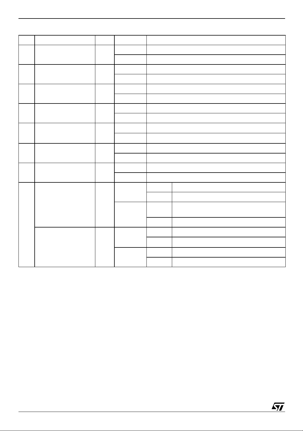
M58WR064ET, M58WR064EB
Table 8. Status Register Bits
Bit Name Type Logic Level Definition
SR7 P/E.C. Status Status
SR6 Erase Suspend Status St atus
’1’ Ready
’0’ Busy
’1’ Erase Suspended
’0’ Erase In progress or Completed
SR5 Erase Status Error
SR4 Program Status Error
SR3
V
PP
Error
Status
SR2 Program Suspend Status Status
SR1 Block Protection Status Error
Bank Write Status Status
SR0
Multiple Word Program
Status (Enhanced
Status
Factory Program mode)
Note: Logic level ’1’ is High, ’0’ is Low.
’1’ Erase Error
’0’ Erase Success
’1’ Program Error
’0’ Program Success
Invalid, Abort
’1’
’0’
V
PP
V
OK
PP
’1’ Program Suspended
’0’ Program In Progress or Completed
’1’ Program/Erase on protected Block, Abort
’0’ No operation to protected blocks
SR7 = ‘0’ Program or erase operation in addressed bank
’0’
SR7 = ‘1’ No Program or erase operation in the device
'1'
SR7 = ‘0’
Program or erase operation in a bank other than
the addressed bank
SR7 = ‘1’ Not Allowed
SR7 = ‘0’ the device is NOT ready for the next word
'1'
SR7 = ‘1’ Not Allowed
SR7 = ‘0’ the device is ready for the next Word
'0'
SR7 = ‘1’ the device is exiting from EFP
24/82

CONFIGURATION REGISTER
The Configuration Register is used to configure
the type of bus access that the memory will perform. Refe r to Rea d Mo des secti on fo r d etai ls on
read operations.
The Configuration Register is set through the
Command Interface. After a Reset or Power-Up
the device is configured for asynchronous page
read (CR15 = 1). T he Configuration Register bits
are described in Table 9. They spe cify the selection of the burst length, burst type, burst X latency
and the Read operation. Refer to Figures 6 and 7
for examples of synchronous burst configurations.
Read Select Bit (CR15)
The Read Select bit, CR15, is used to switch between asynchronous an d sync hronous B us Read
operations. When the Read Se lect bit is set to ’1’,
read operations are asynchronous; when the
Read Select bit is set to ’0’, read o perations are
synchronous. Synchronous Burst Read is supported in both parameter and main blocks and can be
performed across banks.
On reset or power-up the Read Sel ect bit is set
to’1’ for asynchronous access.
X-Latency Bits (CR13-CR11)
The X-Latency bits are used during Synchronous
Read operations to set the number of clock cycles
between the address bei ng latched and the first
data becoming available. For correct operation the
X-Latency bits can only assume the values in Table 9, Configuration Register.
The correspondence be tween X-Latency settings
and the maximum sustainable freq uency must be
calculated taking into account some system parameters. Two conditions must be satisfied:
1. Depending on whether t
AVK_CPU
or t
DELAY
is
supplied either one of the following two
equations must be satisfied:
(n + 1) t
(n + 2) tK ≥ t
≥ t
K
ACC
ACC
- t
AVK_CPU
+ t
DELAY
+ t
+ t
QVK_CPU
QVK_CPU
2. and also
> t
t
K
KQV
+ t
QVK_CPU
where
n is the chosen X-Latency configuration code
is the clock period
t
K
t
AVK_CPU
is clock to address valid, L Low, or E
Low, whichever occurs last
t
is address valid, L Low, or E Low t o clock,
DELAY
whichever occurs last
t
QVK_CPU
is the data setup time required by the
system CPU,
is the clock to data valid time
t
KQV
is the random access time of the device.
t
ACC
M58WR064ET, M58WR064EB
Refer to Figure 6, X-Latency and Data Output
Configuration Example.
Wait Polarity Bit (CR10)
In synchronous burst mode the W ait signal indicates whether the output data are valid or a WAIT
state must be inserted. The Wait Polarity bit is
used to set the po larity of the Wait signal. When
the Wait Polarity bit is set to ‘0’ the Wait signal is
active Low. When the Wait P ola rity bit is s et t o ‘ 1’
the Wait signal is active High (default).
Data Output Configuration Bit (CR9)
The Data Output Configuration bit determines
whether the output remains valid for one or two
clock cycles. When the Data Output Configuration
Bit is ’0’ the output data is valid for one clock cycle,
when the Data Output Configuration Bit is ’1’ the
output data is valid for two clock cycles.
The Data Output Configuration depends on the
condition:
■ t
> t
K
where tK is the clock period, t
setup time required by the s ystem CPU and t
is the clock to data valid time. If this condition is not
satisfied, the Data Output Configuration bit should
be set to ‘1’ (two clock cycles). Refer to Figure 6,
X-Latency and Data Output Configuration Example.
Wait Confi guration Bit (C R 8)
In burst mode the Wait bit controls the timing of the
Wait output pin, WAIT. When WAIT is asserted,
Data is Not Valid and when WAIT is deasserted,
Data is Valid. When the Wait bit is ’0’ the Wait output pin is asserted during the wait state. When the
Wait bit is ’1’ (default) the Wait output pin is asserted one clock cycle before the wait state.
Burst Type Bit (CR7)
The Burst Type bit is used to configure the sequence of addres ses read as sequential or interleaved. When the Burst Type bit is ’0’ the memory
outputs from interleaved addresses; when the
Burst Type bit is ’1’ (default) the mem ory outputs
from sequential addresses. Se e Tables 10, Burst
Type Definition, for the sequence of addresses
output from a given starting address in each mode.
Valid Clock Edge Bit (CR6)
The Valid Clock Edge bit, CR6, is used to configure the active edge of the Clock, K, during Synchronous Burst Read operations. When the Valid
Clock Edge bit is ’0’ the falling edge of the Clock is
the active edge; when the Vali d Clock Edge bit is
’1’ the rising edge of the Clock is active.
Wrap Burst Bit (CR3)
The burst reads can be confined inside the 4 or 8
Word boundary (wrap) or o vercome t he b oundary
KQV
+ t
QVK_CPU
QVK_CPU
is the data
KQV
25/82
 Loading...