

64 Mbit (4Mb x16, Mux I/O, Dual Bank, Burst)
■ SUPPLY VOLTAGE
DD
=V
–V
Erase and Read
–V
■ MULTIPLEXED ADDRESS/DATA
■ SYNCHRONOUS / ASYNCHRONOUS READ
= 12V for fast Program (optional)
PP
– B urs t mode Read: 54MHz
– P age mode Read (4 Words Page)
– Random Access: 100ns
■ PROGRAMMING TIME
– 10µs by W ord typical
– Two or four words program ming option
■ MEMORY BLOCKS
– Dual Bank Memo ry Array: 16/48 Mbit
– Parameter Blocks (T op or Bottom location)
■ DUAL OPERATIONS
– Read within one Bank while Program or
Erase within the other
– No delay between Read andWrite operations
■ PROTECTION/SECURITY
– A ll Blocks protected at Power-up
– Any combination of Blocks can be protected
– 64 bit unique device identifier
– 64 bit user programmable OTP cells
– One parameter block permanently l oc ka ble
■ COMMON FLASH INTERFACE (CFI)
■ 100,000 PROGRAM/ER ASE CYCLES per
BLOCK
■ ELECTRONIC SIGNATURE
– Manufacturer Code: 20h
– Top Device Code, M58MR064C: 88DCh
– B ottom Device Code, M58MR064D: 88DDh
= 1.65V to 2.0V for Program,
DDQ
M58MR064C
M58MR064D
1.8V Supply Flash Memory
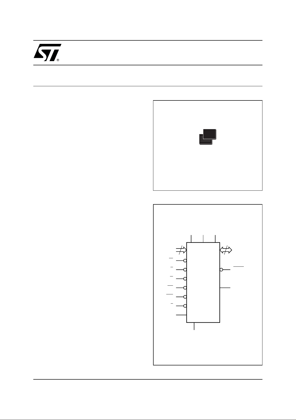
FBGA
TFBGA48 (ZC)
10 x 4 ball array
Figure 1. Logic Diagram
V
V
DDQVPP
DD
A16-A21
W
RP
WP
6
E
G
L
K
M58MR064C
M58MR064D
V
SS
16
ADQ0-ADQ15
WAIT
BINV
AI90087
1/52March 2002
M58MR064C, M58MR064D
Figure 2. TFBGA Connections (Top view th rough package)
87654321
A
B
C
D
E
F
G
H
DU
DU
DU
DU
DDQ
SS
ADQ15
A21
ADQ14
V
SS
SS
KWAIT
DD
ADQ13 ADQ12
V
WV
WPRPBINVLA20A16V
ADQ2ADQ3ADQ6ADQ7V
ADQ10ADQ11ADQ4ADQ5V
109
A19
A18
DDQ
A17
ADQ8
ADQ1
PP
ADQ9
V
1211
DU
NC
V
E
SS
G
ADQ0
DU
1413
DU
DU
AI90088
DESCRIPTION
The M58MR064 is a 64 Mbit non-v olatile Flash
memory that may be erased electrically a t block
level and programmed in-system on a Word-byWord basis using a 1.65V to 2.0V V
supply for
DD
the circuitry. For Program and Erase operations
the necessary high voltages are generated internally. The device suppo rts synchronous burst read
and asynchronous read from all the blocks of the
memory array; at power-up the device is configured for page mode read. In synchronous burst
mode, a new data is output at e ach clock cycle for
frequencies up to 54MHz.
The a rray matrix organization allows each block to
be erased and reprogrammed without affecting
other blocks. All blocks are protected against programming and erase at Power-up.
Blocks can be unprotected to make changes i n the
application and then re-protected.
A parameter block "Secu rity bl ock" can be permanently protected against programming and erasing
2/52
in order to increase the data security. An optional
12V V
power supply is provided to speed up the
PP
program phase at costumer production. An internal command interface (C.I.) decodes the instructions t o access/modify the memory content. The
program/erase controller (P/E.C.) automatically
executes the algorithms taking care of the tim ings
necessary for program and erase operations. Two
status registers indicate the state of each bank.
Instructions for Read Array , Read Elec tronic Signature, Read Status Register, Clear Status Register, Write Read Configuration Register, Program,
Block Erase, Bank Erase, Program Suspend, Program Resume, Erase Suspend, Erase Resume,
Block Protect, Bloc k Unprotect, Block Locking,
Protection P r ogram, CFI Query, are written to the
memory through a Com mand Interface ( C.I.) using
standard micro-processor write timings.
The memory is offered in TFBGA48, 0.5 mm ba ll
pitch packages and it is supplied with all t he bits
erased (set to ’1’).
M58MR064C, M58MR064D
Table 1. Signal Names
A16-A21 Address Inputs
ADQ0-ADQ15
E
G
W
RP
Data Input/Outputs or Address
Inputs, Command Inputs
Chip Enable
Output Enable
Write Enable
Reset/Power-down
Organization
The M58M R064 is organized as 4Mb by 16 bits.
The first sixteen address lines are multiplexed with
the Data Input/Output signals on the mul tiplexed
address/data bus A D Q0-ADQ15. The remaining
address lines A16-A21 are the MSB addresses.
Chip Enable E
inputs provide memory control.
W
, Outp ut Enable G and WriteEnable
The clock K input synchronizes the mem ory to the
microprocessor during burst read.
Reset RP
is used to reset all t he memory circuitry
and to set the chip inpower-down mode if a proper
setting of the Read Configuration Register en-
WP
K Burst Clock
L
Write Protect
Latch Enable
ables this function.
output indicates to the microprocessor the
WAIT
status of the memory during the burst mode operations.
Memory Blocks
WAIT
BINV Bus Invert
V
DD
V
DDQ
V
PP
Wait Data in Burst Mode
Supply Voltage
Supply Voltage for Input/Output
Buffers
Optional Supply Voltage for
Fast Program & Erase
The d ev ice features asymmetrically blocked architecture. M58MR064 has an array of 135 blocks
and is di vided into two banks A and B, prov iding
Dual Bank operations. Whil e programming or
erasing in Bank A, read operations are possible
into Bank B or vice versa. Only one bank at the
time is allowed to be in progra m or erase mode. It
is possible to perform burst reads that cross bank
boundaries.
The memory features an erase suspend allowing
reading or programming in another block. Once
V
SS
DU Don’t Use as Internally Connected
NC Not Connected Internally
Ground
suspended the erase can be resumed. Program
can be suspended to read data in another block
and then res umed. The B ank Size and sectorizationaresummarizedinTable3.ParameterBlocks
are located at the top of the memory address
space for the M58MR064C, and at the bottom for
the M58MR064D. The memory maps are shown in
Figure 3.
Table 2. Absolute Maximum Ratings
Symbol Parameter Value Unit
T
A
Ambient Operating Temperature
(1)
(2)
–40 to 85 °C
T
BIAS
T
STG
(3)
V
IO
V
DD,VDDQ
V
PP
Note: 1. Except for the rating "Operating Temperature Range", stresses above those listed in the Table "Absolute Maximum Ratings" may
cause permanent damage to the device. These are stress ratings only and operation of the device at these or any other conditions
above those indicated in the Operating sections of this specification is not implied. Exposure to Absolute Maximum Rating conditionsforextended periods mayaffectdevice reliability.Referalso to theSTMicroelectronicsSURE Program andotherrelevantquality documents.
2. Depends on range.
3. Minimum Voltage may undershoot to –2V during transition and for less than 20ns.
Temperature Under Bias –40 to 125 °C
Storage Temperature –55 to 155 °C
Input or Output Voltage
Supply Voltage –0.5 to 2.7 V
Program Voltage –0.5 to 13 V
–0.5 to V
DDQ
+0.5
V
3/52
M58MR064C, M58MR064D
The architecture includes a 128 bits Protection
register t hat is di vided into two 64-bits segments.
In the f irst one is written a unique device number,
while the second one is programmable by the user. The user programmable segment can be permanently protec ted programming the bit 1 of the
Protection Lock Register (see protection register
and Security Block). The parameter block (# 0) is
a security block. It can be permanently protected
Table3.BankSizeandSectorization
Bank Size Parameter Blocks Main Blocks
Bank A 16 Mbit 8 blocks of 4 KWord 31 blocks of 32 KWord
Bank B 48 Mbit - 96 blocks of 32 KWord
Figure 3. Memory Map
Top Boot Block
Address lines A21-A0
000000h
007FFFh
Bank B
512 Kbit or
32 KWord
Total of 96
Main Blocks
by the user programmingthe bit2 of the Protection
Lock Register.
Block protection against Program or Erase provides additional data security. All blocks are protected and unlocked at Power-up. Instructions are
provided to protect o r un-protect any block in t he
application. A second register locks the protection
status while WP
islow (see BlockLocking descrip-
tion).
Bottom Boot Block
Address lines A21-A0
000000h
000FFFh
64 Kbit or
4 KWord
Total of 8
Parameter
Blocks
Bank A
2F8000h
2FFFFFh
300000h
307FFFh
3F0000h
3F7FFFh
3F8000h
3F8FFFh
3FF000h
3FFFFFh
512 Kbit or
32 KWord
512 Kbit or
32 KWord
512 Kbit or
32 KWord
64 Kbit or
4 KWord
64 Kbit or
4 KWord
Total of 31
Main Blocks
Total of 8
Parameter
Blocks
Bank A
Bank B
007000h
007FFFh
008000h
00FFFFh
0F8000h
0FFFFFh
100000h
107FFFh
3F8000h
3FFFFFh
64 Kbit or
4 KWord
512 Kbit or
32 KWord
Total of 31
Main Blocks
512 Kbit or
32 KWord
512 Kbit or
32 KWord
Total of 96
Main Blocks
512 Kbit or
32 KWord
AI90089
4/52

M58MR064C, M58MR064D
SIGNAL DESCRIPTIONS
See Figure 1 and Table 1.
Address Inputs or Data I nput/Output (ADQ0ADQ15). When Chip Enable E
put Enable G
is at VIHthe multiplexed address/
is at VILand Out-
data bus is used to input addresses for the memory array, data to be program med in the memory array or commands to be written to the C.I. T he
address inputs for the memory array are latched
on the rising edge of Latch Enable L
latch is trans parent when L
is at VIL. In synchro-
. The address
nous operat ions the address is also latched on the
first rising/falling edge of K (depe nding on clock
configuration) when L
is low. Bot h input dat a and
commands are latched on the rising edge of Write
Enable W
able G
. When Chip Enable E and Output En-
are at VILthe address/data b us outputs
data from the Memory Array, the Electronic Signature Manufacturer or Dev ice codes , the Block Protection status the Read Configuration Register
status, the protection register or the Status Register. The address/data bus is high impedance when
the chip is des elected, Output Enable G
or RP
is at VIL.
is at VIH,
Address Inputs (A16-A21). ThefiveMSBaddresses of the memory array are latched on the
rising edge of Latch Enable L
. In synchronous operation these inputs are also latched on the first
rising/falling edge of K (depending on clock configuration) when L
Chip Enable (E
is low.
). The C hip Enable input a ctivates the memory control logic, input buffers, decoders and sense amplifiers. E
at VIHdeselects
the m emory and reduces t he power consumption
to the standby level. E
canalsobeusedtocontrol
writing to the command register and to the memory array, while W
Output Enable (G
remains at VIL.
). The Output Enable gates the
outputs through the data buf fers during a read operation. When G
is at VIHthe outputs are High im-
pedance.
WriteEnable(W
). This input controls writing to
theCommand Register and Dat a latches. Data are
latched on the rising edge of W
Write Protect (WP
). This input gives an addition-
.
al hardware protection level against program or
erase when pulled at V
, as described in the Block
IL
Lock instruction des cripti on.
Reset/Power-down Input (RP
). The RP input
provides hardware reset of the memory, and/or
Power-down functions, depending on the Read
Configuration Regi ster status. Reset/Power-down
of the memory is achieved by pul ling RP
to VILfor
at least t
. When the reset pulse is given, the
PLPH
memory wi ll recover from Power-down (when enabled) in a minimum of t
PHEL,tPHLL
or t
PHWL
(see
Table 31 and Figure 15) after the rising edge of
RP
. Exit from Reset/Power-down changes the
contents of the Read Configuration Register bits
14 and 15, setting the memory in async hronous
page mode read and power save function disabled. All b locks are protected and unlocked after
a Reset/Power-down.
Latch Enable (L
). L latches the address bits
ADQ0-ADQ15 and A16-A2 1 on its rising edge.
The address latch is transparent when L
is at V
and it is inhibited w hen L is at VIH.
Clock (K). The c lock input synchronizes the
memory to the micro controller during burst mode
read operation; the address is latched on a K edge
(risingor falling, according to the configurat ion settings) when L
is at VIL. K is don't care during asyn-
chronous page mode read and in write operations.
Wait (WAIT
). WAIT is an output signal used dur-
ing burst mode read, indicating whether the data
on the output bus are valid or a wait state must be
inserted. This output is high impedance when E
G
arehighorRPis at VIL, and can be configured
or
to be active during the wait cycle or one c lock cycle in advance.
Bus Invert (BINV). BINV is an input/output signal
used to reduce the amount of power needed to
switch the ex ternal address/data bus. The power
saving is achieved by inverting the data output on
ADQ0-ADQ15 every time this gives an advantage
in terms of number of toggling bits. In burst mode
read, each new data output from the memory is
compared with the previou s data. If the number of
transitions required on the data bus is in excess of
8, the data is inverted and the BINV signal will be
driven by the memory at V
to inform the receiv-
OH
ing system that data mus t be inverted before any
further process ing. By doing so, the actual tr ans itions on the data bus will be less than 8.
In a similar way, when a command is given, BINV
may be driven by the system at V
to inform the
IH
memory that the data input must b e inverted.
Like the other input/output pins, BINV is high im-
pedance when the chip is deselected, output enable G
is at VIHor RP is at VIL;whenusedasan
input, BINV must follow t he same set-up and hold
timings of the data inputs.
V
and V
DD
is the main power supply for all operations
V
DD
(Read, P rogram and Erase). V
Supply Voltage (1.65V to 2.0V).
DDQ
is the supply
DDQ
voltage for Input and Output.
IL
5/52

M58MR064C, M58MR064D
VPPProgram Supply Voltage (12V). VPPis both
a cont rol input and a power supply pin. The two
functions are selected by the voltage range applied to the pin; if V
(0 to 2V) V
PP
is kept ina low voltage ra nge
PP
is seen as a control input, and the
current absorption is lim ited to 5µA (0.2µA typical).
In this case with V
PP=VIL
protection against program or erase; with V
V
these functions are enab led (see Table 26).
PP1
value is only sampled during p rogram or
V
PP
we obtain an absolute
PP
erase write cycle s; a change in its value after the
operation has been started does not have any effect and program or erase are carried on regularly.
If V
is used in the 11.4V to 12.6V range (V
PP
then the pin acts as a power supply (see Table
26). This supply voltage must remain stable as
long as program or erase are running. In read
mode the current sunk is less then 0.5mA, while
during program and erase operations the current
=
may increase up to 10mA.
Ground. VSSis the reference for all the volt-
V
SS
age measurements.
PPH
)
6/52
M58MR064C, M58MR064D
DEVICE OPERATIONS
The f ollowing operations can be performed using
the appropriate bus cycles: Address Latch, Read
Array (Random, and Page Modes), Write command, Output Disable, Standby, res et/Powerdown and Block Locking. See Table 4.
Address Latch. In asynchronous operation, the
address is latched on the rising edge of L
input. In
burst mode the address is la tched either onthe rising edge of L
or on the first rising/falling edge of K
(depending on configuration settings) when L
low.
Read. Read operations are used to output the
contents of the Memory A rray , the Electronic Sig-
Table 4. User Bus Operations
(1)
nature, the Status Register, the CFI, the Block
Protection Status, the Read Configurat ion Register status and the Protection Register.
Read operation of the Memory Array may be performed in asynchronou s page mode or synchronous burst mode. In asynchronous page mode
data is internally read and stored in a page buffer.
The page has a size of 4 words and is addressed
by ADQ0 and ADQ1 ad dres s inputs.
According to the device configuration the f ollowing
is
Read operat ions: Electronic Signature - Status
Register - CFI - Block Protection Status - Read
Configuration Register Status - Protection Register must be accessed as asynchronous read or as
single synchronous read (see Figure 4).
Operation E G W L RP WP ADQ15-ADQ0
V
Address Latch
Write
Output Disable
Standby
V
IL
V
IL
V
IL
V
IH
V
IH
V
IH
V
IH
V
IH
V
IL
V
IH
XX X
Reset / Power-down X X X X
Block Locking
Note: 1. X = Don't care.
V
IL
XX X
IL
(rising edge)
V
IH
V
IH
V
IH
V
IH
V
IH
V
IH
V
IL
V
IH
V
IH
V
IH
V
IH
X
X
V
IL
Address Input
Data Input
Hi-Z
Hi-Z
Hi-Z
X
(3)
(1)
ADQ0
Table 5. Read Electronic Signature (AS and Read CFI instructions)
Code Device E
Manufacturer Code
M58MR064C
V
IL
V
IL
G W
V
IL
V
IL
ADQ1
V
IH
V
IH
V
IL
V
IL
Device Code
M58MR064D
Note: 1. Addresses are latched on the rising edge of L input.
2. EA means Electronic Signature Address (see Read Electronic Signature)
3. Value during address latch.
V
IL
Table 6. Read Block Protection (AS and Read CFI instructions)
Block Status E
Protected and unlocked
Unprotected and unlocked
Protected and locked
Unprotected and locked
Note: 1. Addresses are latched on the rising edge of L input.
2. AlockedblockcanbeunprotectedonlywithWP
3. Value during address latch.
4. BA means Block Address. First cycle command address should indicate the bank of the block address.
(2)
V
IL
V
IL
V
IL
V
IL
V
IL
G W
V
IL
V
IL
V
IL
V
IL
at V
IH.
V
IH
V
IH
V
IH
V
IH
V
IH
V
ADQ1
V
V
V
V
IL
(1)
(3)
ADQ0
IH
IH
IH
IH
(3)
V
IL
V
IH
V
IH
(3)
V
IL
V
IL
V
IL
V
IL
Other
Address
(2)
EA
(2)
EA
(2)
EA
Other
Address
(4)
BA
(4)
BA
(4)
BA
(4)
BA
(2)
ADQ15-0
0020h
88DCh
88DDh
ADQ15-0
0001
0000
0003
0002
7/52
M58MR064C, M58MR064D
Table 7. Read Protection Register (RSIG and RCFI Instruction)
(1)
Word E G W A21-17 ADQ15-8 ADQ7-0 ADQ15-8 ADQ7-3 ADQ2 ADQ1 ADQ0
Lock
Unique
ID 0
Unique
ID 1
Unique
ID 2
Unique
ID 3
OTP 0
OTP 1
OTP 2
OTP 3
Note: 1. Addresses are latched on the rising edge of L input.
V
ILVILVIH X
V
ILVILVIH X
V
ILVILVIH X
V
ILVILVIH X
V
ILVILVIH
V
ILVILVIH
V
ILVILVIH
V
ILVILVIH
V
ILVILVIH
2. X = Don't care.
(2)
(2)
(2)
(2)
(2)
X
(2)
X
(2)
X
(2)
X
(2)
X
(2)
X
(2)
X
(2)
X
(2)
X
(2)
X
(2)
X
(2)
X
(2)
X
(2)
X
80h 00h 00000B
Security
prot.data
81h ID data ID data ID data ID data ID data
82h ID data ID data ID data ID data ID data
83h ID data ID data ID data ID data ID data
84h ID data ID data ID data ID data ID data
85h OTP data
86h OTP data
87h OTP data
88h OTP data
OTP
data
OTP
data
OTP
data
OTP
data
OTP
data
OTP
data
OTP
data
OTP
data
OTP
prot.data
OTP
data
OTP
data
OTP
data
OTP
data
0
OTP
data
OTP
data
OTP
data
OTP
data
Table 8. Dual Bank Operations
(1,2,3)
Commands allowed in the other bank
Status of one
bank
Read
Array
Read
Status
Read
ID/CFI
Program
Erase/
Erase
Resume
Program
Suspend
Erase
Suspend
Protect
Unprotect
Idle Yes Yes Yes Yes Yes Yes Yes Yes
Reading ––––––––
Programming Yes Yes Yes ––––Yes
Erasing Yes Yes Yes ––––Yes
Program
Suspended
Erase
Suspended
Note: 1. For detailed description of command see Table 33 and 34.
2. There is a status register for each bank; status register indicates bank state, not P/E.C. status.
3. Command must be written to an address within the block targeted by that command.
YesYesYes––––Yes
Yes Yes Yes Yes – Yes – Yes
8/52
M58MR064C, M58MR064D
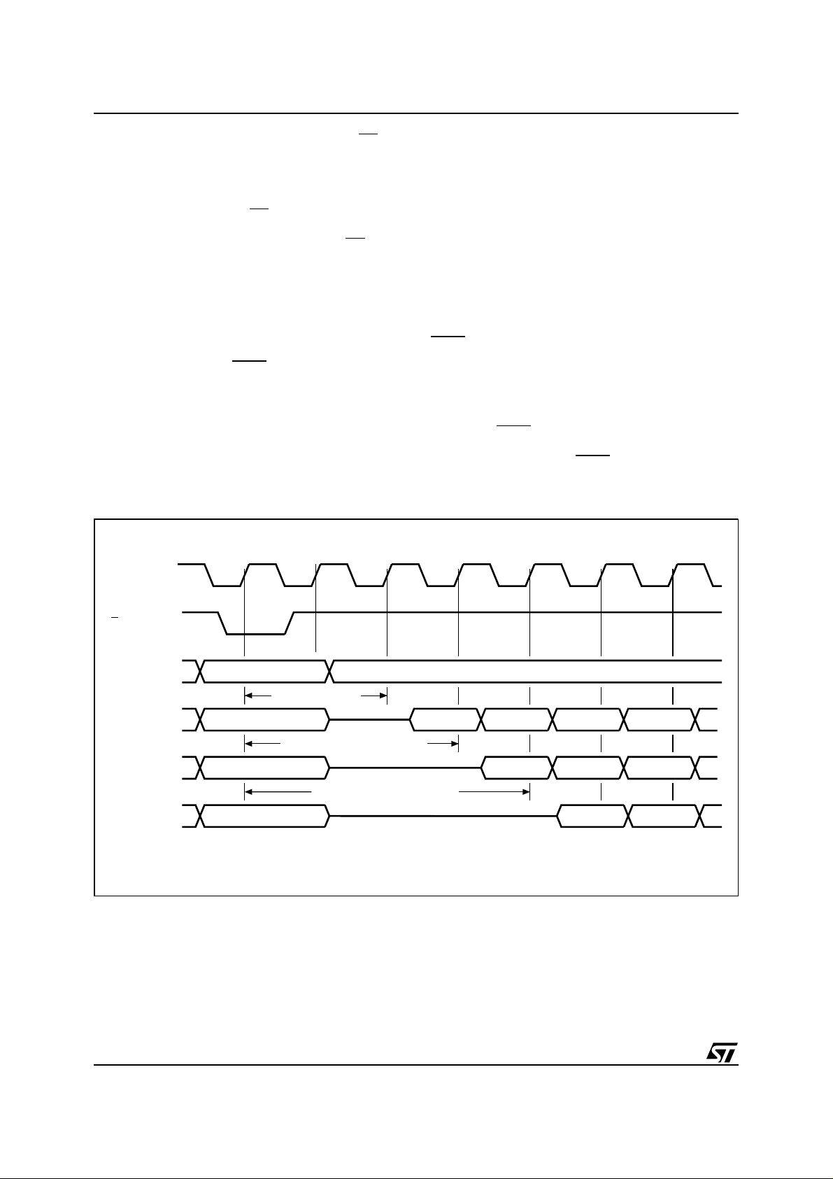
Figure 4. Single Synchronous Read Sequence (RSIG, RCFI, RSR instructions)
K
L
A21-A16
ADQ15-ADQ0
ADQ15-ADQ0
ADQ15-ADQ0
VALID ADDRESS
CONF. CODE 2
VALID ADDRESS VALID DATA NOT VALID
CONFIGURATION CODE 3
VALID ADDRESS VALID DATA
CONFIGURATION CODE 4
VALID ADDRESS NOT VALID
Both Chip E nable E and Output Enable G must be
at V
in order to read the output of t he memory.
IL
Read array is the default state o f the device when
exiting power down or after power up.
Burst Read. The device also supports a burst
read. In this mode a burst sequence is started at
the first clock edge (rising or falling according to
configuration settings) after the falling edge of L
After a configurable delay of 2 to 5 clock cycles a
new data is output at each clock cycle. The burst
sequence may be configured for linear or interleaved order and for a length of 4, 8 words or for
continuous burst mode. Wrap and no-wrap modes
are also supported.
AWAIT
signal may be ass erted to indicate to the
system that an output delay wil l occur. This delay
will depend on the starting address of the burst sequence; t he worst case delay will occur w hen the
sequence is crossing a 64 word boundary and the
starting address w as at the end of a four word
boundary. See the Write Read Configuration Register (CR) Instruction for more details on all the
possible settings for the synchronous burst read
(see Table 14). It is possible to perform burst read
across bank boundary ( all banks in read array
mode).
Write. Wri te operations are used to give I ns truction Commands to the memory or to latch Input
Data to be programmed. A w rite operation is initiated when Chip Enable E
at V
with Output Enable G at VIH. Addresses are
IL
latched on the rising edge of L
put Data are latched on the rising edge of W
and Write Enable W are
. Co mm ands and In-
or E
whichever occ urs first. Noise pulses of less than
5ns typical on E
NOT VALID
NOT VALID
VALID DATA
,Wand G signals do not start a
NOT VALID
NOT VALID
write cycle. Write ope rations are asynchronous
and clock is ignore d during write.
Dual Bank Op erations. The Dual Bank allows to
run different operations simultaneously in the two
banks. It is possible to read array data from one
bank while the other is programming, erasing or
reading any data (CFI, status register or electronic
.
signature).
Read and write cycles c an be initiated for simulta-
neous operations in different banks without any
delay. Only one bank at a tim e is allowed to be in
program or erase mode, while the other must be in
one of the rea d modes (see Table 8).
Commands m ust be written to an address within
the block targeted by that command.
Output Disable. The data outputs are high impedance when t he Output Enable G
Write Enable W
at VIH.
is at VIHwith
Standby. The memory is in standby when Chip
Enable E
is at VIHand the P /E. C. is idle. The power consumption is reduced to t he standby level
and the outputs are high impedance, inde pendent
of the Output Enable G
or Write Enable W inputs.
Automatic Standby. When in Read mode, after
150ns of bus inactivity and when CMOS levels are
driving the addresses, the chip automatically enters a pseudo-standby mode where consumption
is reduced to the CMOS standby value, while outputs still drive the bus. The automatic standby feature is not available when th e dev ice is configured
for synchronous burst mode.
AI90090
9/52
M58MR064C, M58MR064D
Table 9. Identifier Codes
Code Address (h) Data (h)
Manufacturer Code Bank Address + 00 0020
Device Code
Top Bank Address + 01 88DC
Bottom Bank Address + 01 88DD
Protected and Unlocked
Block Protection
Die Revision Code Bank Address + 03
Read Configuration Register Bank Address + 05
Lock Protection Register Bank Address + 80
Protection Register
Note: 1. DRC means Die Revision Code.
CR means Read Configuration Register.
LPR means Lock Protection Register.
PR means Unique Device Number and User Programmable OTP.
Reset/Power-down. The memory is in Powerdown when the Read Configuration Register is set
for Power-down and RP
sumption is reduced to the Power-down level, and
Outputs are in high impedanc e, independent ofthe
Chip Enable E
inputs. The memory is in reset when the Read
W
, Output Enable G or Write Enable
Configuration Register is set for Reset and RP
at VIL
. The power cons umption is the same of the
standby and the outputs a re in high impedance.
After a Reset/Power do wn the device defaults to
Unprotected and Unlocked 0000
Protected and Locked 0003
Unprotected and Locked 0002
Bank Address + 02
Bank Address + 81
Bank Address + 88
Block Locking. Any combination of blocks can
be temporarily protected against Program or
is at VIL. The p ower con-
Erase by setting the lock register and pulling WP
to VIL. The following summarizes the locking operation. All blocks are prot ec ted on power-up. They
can then be unprotected or protected with the Unprotect and Protect c ommands. T he Lock com-
is
mand protects a block and prevents it from being
unlocked when WP
overridden. Lock is cleared only w hen the device
is reset o r powered-down (see Protect instruction).
read array mode, the status register is set to 80h
and the read configuration register defaults to
asynchronous read.
0001
(1)
DRC
(1)
CR
(1)
LPR
(1)
PR
=0.WhenWP= 1, Loc k is
10/52
M58MR064C, M58MR064D
INSTRUCTIONS AND COMMANDS
Eighteen instructions are available (see Tables 10
and 11) t o perform Read Memory Array, Read Status Re giste r, Read Electronic Signature, CFI Query,Block Erase, Bank Erase, Program,Tetra Word
Program, Double Word Program, Clear Status
Register, Program/Erase Suspend, Pro gram/
Erase Resume, Block Protect, B lock Unprotect,
Block Lock , Protection Register Program, Read
Configuration Register and Lock Protection Program.
Status R egister output may be read at any time,
during programming or erase, to monitor the
progress of the operation.
An internal Command Interface (C.I.) decodes the
instructions while an internal Program / Erase Controller (P/E.C.) handles all timing and verifies the
correct execution of the Program and Erase instructions. P/E.C. provides a Status Regi ster
whose bits indicate operation and exit status of the
internal algorithms. The Com mand Interface is reset to Read Array when power is first applied,
when exiting from Reset or whenever V
than V
. Command sequence must be followed
LKO
DD
is lower
exactly. Any invalid combination of commands will
reset the device to Read Array.
Read (RD)
The Read instruction consists of one write cycle
(refer to Device Operat ions section) and places
the addressed bank in Read Array mode. When a
device reset occurs, the memory is in Read Array
as default. A read array command will be ig nored
while a bank is programming or erasing. However
inthe other bank a read array command wi ll be accepted.
Read Status Register (RS R)
A bank's Status Register indicates when a program or erase operation is complete and th e success or failure of operation itself. Issue a Read
Status Register Instruction (70h) to read t he Status Register content of the addressed bank. The
status of the other bank is not affect ed by the command. The Read Status Regist er instruction may
be issued at any t ime, also when a Program/Erase
operation is ongoing. The following Read operations output the content of the Status Register of
the addressed bank. The S tatus Register is
latched on the falling edge of E
canbereaduntilE
G
must be toggled to update the latched data.
or G returns to VIH. Either E or
or G signals, and
Read Electronic Signatu re (RSIG)
The Read Electronic Signature instruction consists of one write c y cle (refer to Dev ice Operat ions
section) giving the command 90h to an address
Table 10. Commands
Hex Code Command
00h Invalid Reset
01h Protect Confirm
03h
10h Alternative Program Set-up
20h Block Erase Set-up
2Fh Lock Confirm
30h Double Word Program Set-up
40h Program Set-up
50h Clear Status Register
55h Tetra Word Program Set-up
60h
70h Read Status Register
80h Bank Erase Set-up
90h Read Electronic Signature
98h CFI Query
B0h Program/Erase Suspend
C0h
D0h
FFh Read Array
Write Read Configuration Register
Confirm
Protect Set-up and Write Read
Configuration Register
Protection Program and Lock Protection
Program
Program/Erase Resume, Erase Confirm
or Unprotect Confirm
within the bank A. A subsequent read in the address of bank A will output the Manufacturer Code,
theDeviceCode,theprotectionStatusofBlocks
of bank A, the Die Revision Code, the Protect ion
Register, or the Read Configuration Register (see
Table 9).
If the first write cycle of Read E lectronic Signature
instruction is issued to an address within the bank
B, a subsequent read in an address of bank B wi ll
output the prot ec ti on Status of Blocks of bank B.
The status of t he other bank is not affected by the
command (see Tabl e 8).
See Tables 5, 6, 7 and 8 for the valid address. The
Electronic Signat ure can be read from the me mory
allowing programming equipment or applications
to aut omatically match their interface to the characteristics of M58MR064C and M58MR06 4D.
11/52
M58MR064C, M58MR064D
Table 11. Ins t ructi ons
Instruction Cyc. Operation
Read
RD
Memory
Array
1+ Write BKA FFh
Address
(1,2)
Data
(3)
Operation
(1)
Read
Address
(1,2)
Read
Address
Data
Data
(3)
RSR
Read Status
Register
1+ Write BKA 70h
Read
RSIG
READ
Electronic
1+ Write EA 90h
Read
Read
(1)
(1)
BKA
EA ED
Signature
RCFI Read CFI 1+ Write CA 98h
Clear Status
CLRS
(5)
Register
1 Write BKA 50h
Read
(1)
CA CD
EE Block Erase 2 Write BA 20h Write BA D0h
BE Bank Erase 2 Write BKA 80h Write BKA D0h
PG Program 2 Write WA 40h or 10h Write WA WD
DPG
Double Word
Program
3 Write WA1 30h Write WA1 WD1
Write WA2 WD2
TPG
Tetra Word
Program
5 Write WA1 55h Write WA1 WD1
Write WA2 WD2
Write WA3 WD3
PROGRAM/ERASE
Write WA4 WD4
Program
PES
Erase
1 Write BKA B0h
Suspend
Program
PER
Erase
1 Write BKA D0h
Resume
BP Block Protect 2 Write BA 60h Write BA 01h
Block
BU
Unprotect
PROTECT
BL Block Lock 2 Write BA 60h Write BA 2Fh
2 Write BA 60h Write BA D0h
Status
Register
CONFIGURATION
12/52
PRP
LPRP
CR
Protection
Register
Program
Lock
Protection
Register
Program
Write Read
Configuration
Register
2 Write PA C0h Write PA PD
2 Write LPA C0h Write LPA LPD
2 Write RCA 60h Write RCA 03h

M58MR064C, M58MR064D
Note: 1. First cycle command address should be the same as the operation's target address. The first cycle of the RD, RSR, RSIG or RCFI
CFI Query (RCFI)
The CFI Query Mode is as sociated to bank A. T he
address of t he first write cycle must be within t he
bank A. The status ofthe other bank is not affected
bythe com mand (see Table 8). Wr iting 98h the device enters the Common Flash Interface Query
mode. Next read operations in the bank A will read
the CFI data. Write a read instruction to return to
Read mode (refer to the C omm on Flash Interface
section).
Clear Status Register (CLS R)
The Clear Status Register uses a single write operation,which resets bits b1, b3, b4 e b5 of the status register. The Clear Status Register is executed
writing the co mm and 50h independently of the applied V
the device returns to read array mode. The Clear
Status Register command clears on ly the status
register of the address ed bank.
Block Erase (EE)
Block erasure sets all the bits within the selected
block to '1'. One block at a time can be erased. It
is not necessary t o pre-program the block as the
P/E.C. will do it automatically before erasing. This
instruction use two w rites cycles. The first command written is the Block Erase Set up command
20h. The sec ond command is the Erase Confirm
command D0h. An address within t he block to be
erased should be given to the mem ory during the
two cycles command. If the second com mand given is not an erase confirm, the status register bits
b4 and b5 a re s et and the instruc tion aborts.
instruction is followed by read operations in the bank array or special register. Any number of read cycles can occur after one command cycle.
2. BKA means Address within the bank;
BA means BlockAddress;
EA means Electronic SignatureAddress;
CA means Common Flash Interface Address;
WA means Word Address;
PA means ProtectionRegister Address (see Table7);
LPA means Lock Protection Register Address (see Table 7);
RCA means Read Configuration Register Address.
3. PD means Protection Data;
CD means Common Flash Interface Data;
ED means Electronic Signature Data;
WD means Data to be programmed at the address location WA;
LPD means Lock protection Register Data
4. WA1, WA2, WA3 and WA4 must be consecutive address differing only for address bits A1-A0.
5. Read cycle after e CLSR instruction will output the memory array.
After w riting the command, the device outputs status register data when any address within the bank
is read. Atthe end of the operation the bank will remain in read status register until a read array command is written.
Status Register bit b7 is '0' while the eras ure is in
progress and '1' when it has completed. After completion the Status Register bit b5 returns '1' if t here
has been an Erase Failure. Status register bit b1
returns'1'iftheuserisattemptingtoeraseaprotected bl ock. Status Register bit b3 ret urns a '1' if
is below V
V
PP
. A s data integrity cannot be guaranteed when
V
IL
. Erase aborts if RP turns to
PPLK
the erase operation is aborted, the erase must be
repeated (see Table 12). A Clear Status Register
voltage. After executing this command
PP
instruction must be issued to reset b1, b3, b4 and
b5 of t he Status Register. During the execution of
the erase by the P/E.C., the bank with the block in
erase accepts onl y the RSR (Read Status Register) and PES (Program/Erase Suspend) instructions. See figure 19 for Erase Flowchart and
Pseudo Code.
Bank Erase (BE)
Bank erase sets all the bits within the s elected
bank to ’1’. It is not necessary to pre-program t he
block as t he P/E.C. wil l do it automat ically before
erasing.
This instruction uses two writes cycles. The first
command writt en is the Bank Erase set-up command 80h. The second command is the Erase
Confirm command D0h. An address within the
bank to be erased should b e given to the memory
during the two cycles command. See the Block
Erase com mand sec tion for status register bit details.
13/52
M58MR064C, M58MR064D
Table 12. Status Register Bits
Mnemonic Bit Name
P/ECS 7 P/ECS
Status
Logic
Level
1 Ready Indicates the P/E.C. status, check during
0 Busy
Definition Note
Program or Erase, and on completion before
checking bits b4 or b5 for Program or Erase
Success.
ESS 6 Erase
ES 5 Erase Status 1 Erase Error ES bit is set to ’1’ if P/E.C. has applied the
PS 4 Program
VPPS 3 V
PSS 2 Program
BPS 1 Block
0 Reserved
Note: Logic level’1’ is VIHand ’0’ is VIL.
Suspend
Status
Status
Status
PP
Suspend
Status
Protection
Status
1 Suspended
In Progress or
0
Completed
0 Erase Success
1 Program Error
Program
0
Success
VPPInvalid,
1
Abort
V
0
1 Suspended
0
1
0
OK
PP
In Progress or
Completed
Program/Erase
on protected
Block, Abort
No operation to
protected blocks
On an Erase Suspend instruction P/ECS and
ESS bits are set to ’1’. ESS bit remains ’1’ until
an Erase Resume instruction is given.
maximum number of erase pulses to the block
without achieving an erase verify.
PS bit set to ’1’ if the P/E.C. has failed to
program a word.
VPPS bit is set if the VPPvoltage is below
when a Program or Erase instruction is
V
PPLK
executed. V
beginning of the erase/program operation.
On a program Suspend instruction P/ECS and
PSS bits are set to ’1’. PSS remains ’1’ until a
Program Resume Instruction is given.
BPS bit is set to ’1’ if a Program or Erase
operation has been attempted on a protected
block.
is sampled only at the
PP
Program (PG)
The Program instruction programs the array on a
word-by-word basis. The first command must be
given to the target block and only one partition can
be programmed at a time; the other partition must
be in one of the read modes or in t he eras e suspended mode (s ee Table 8).
This instruction uses two write cycles. The first
command written is the Program Set-up c ommand
40h (or 10h). A second write operation latches the
Address and the Data to be written a nd starts the
P/E.C.
Read operations in the targeted bank output the
Status Register content after the programmi ng
has started.
The Status Register bit b7 returns '0' while the programming is in progress and '1' when it has completed. After completion the Status register bit b4
returns'1' if there has been a Program Failure (s ee
14/52
Table 12). Status register bit b1 returns '1' if the
user is attempting to pro gram a protected block.
Status Register bit b3 ret urns a '1' if V
V
. Any attempt to write a ’1’ to an already pro-
PPLK
is below
PP
grammed bit will result in a program fail (status
register bit b4 set) if V
nored if V
PP=VPP1
PP
.
Programming aborts if RP
=V
goes to VIL.Asdatain-
and will be ig-
PPH
tegrity cannot be guaranteed when the program
operation is aborted, the block contain ing the
memory location must be eras ed and reprogrammed. A Clear Status Register instruction
must be issue d to reset b5, b4, b3 and b1 of the
Status Register.
During the execution of the program by the P/E.C.,
the bank in programming accepts only the RSR
(Read Status Register) and PES (Program/Erase
Suspend) instructions. S ee Figure 16 for Program
Flowchart and Pseudo Code.
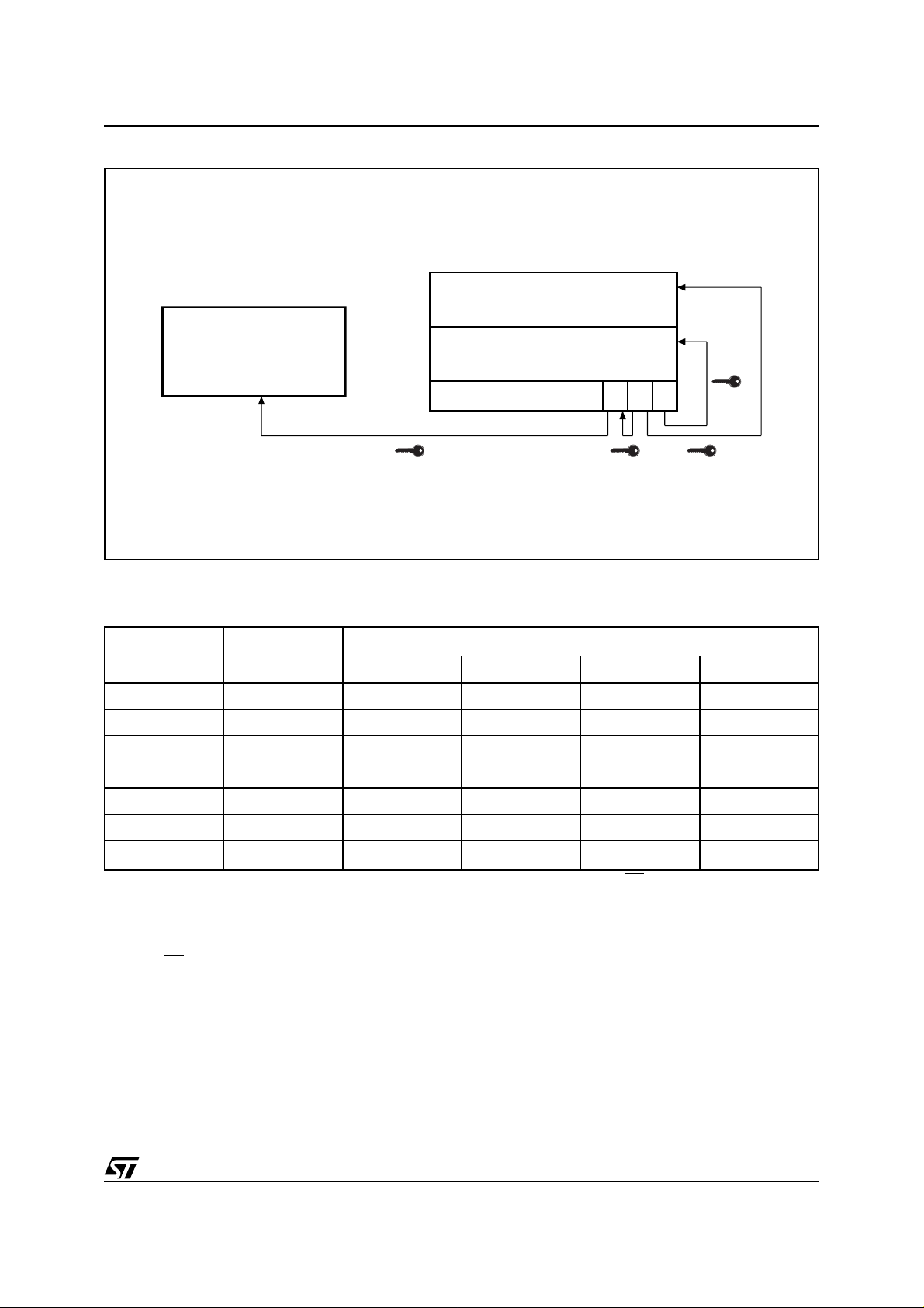
Figure 5. Security Block Memory Map
Parameter Block # 0
88h
85h
84h
81h
80h
M58MR064C, M58MR064D
User Programmable OTP
Unique device number
Protection Register Lock 2 1 0
AI90091
Table 13. Protection States
(2)
Current State
(WP, DQ1, DQ0)
Program/Erase
Allowed
(1)
Next State After Event
(3)
Protect Unprotect Lock WP transition
100 Yes 101 100 111 000
101 No 101 100 111 001
110 Yes 111 110 111 011
111 No 111 110 111 011
000 Yes 001 000 011 100
001 No 001 000 011 101
011No011011011
Note: 1. Allblocksare protectedatpower-up,sothedefaultconfigurationis001 or 101 accordingto WP status.
2. Current state and Next state gives the protection status of a block. The protection status is defined by the write protect in and by
DQ1 (= 1 for a locked block) and DQ0 (= 1 for a protected block) as read in the Read Electronic Signature instruction with A1 = V
and A0 = VIL.
3. Next state is the protection status of a block after aProtect orUnprotect or Lock command has been issued or after WP
its logic value.
4. A WP
transition to VIHon a locked block will restore the previous DQ0 value, giving a 111 or 110.
111 or 110
(4)
IH
has changed
15/52

M58MR064C, M58MR064D
Double W ord Program (DPG)
Thisfeature is offered to improve the programmi ng
throughput, writing a page of two adjacent words
in parallel. The first command mu st be given to the
target block and only one partition can be programmed at a time; the other partition must be in
one of t he read modes or in the erase suspended
mode (see Table 8).
The two words must differ only for the address A0.
Programming should not be attempted when V
is not atV
if V
is below V
PP
. The operation can also be executed
PPH
but result could be uncertain.
PPH
PP
These instruction uses three write cycles. The first
command written is the Double Word Program
Set-Up command 30h. A sec ond write operation
latches the Address and the Data of the first word
to be written, the third w rite operation latche s the
Address and the Data of the second word to be
written and starts the P/E.C. (see Table 11).
Read operations in the targeted bank output the
Status Register content after the programmi ng
has sta rted. The Status Register bit b7 returns '0'
while t he programming is in progress and '1' when
it has completed. After completion the Status register bit b4 returns '1' if there has been a Program
Failure. Status register bit b1 returns '1' if the user
is attempting to program a pro tected block. Status
Register bit b3 returns a '1' if V
is below V
PP
PPLK
Any attempt to write a ’1’ t o an already programmed bit will result in a program fail (status
register bit b4 set). (See Table 12).
Programming aborts if RP
goes to VIL.Asdataintegrity cannot be guaranteed when the program
operation is aborte d, the memory location must be
erased and reprogramm ed. A Clear Statu s Register instruction must be iss ued to reset b5, b4, b3
and b1 of the Stat us Register. D uring the execution of the program by the P/E .C., the bank in programming accepts only the RSR (Read Status
Register) instruction. See Figure 17 for Doub le
Word Program Flowchart and Pseudo c ode.
Tetra Word Program (TPG)
Thisfeature is offered to improve the programmi ng
throughput, writing a page of four adjacent words
in parallel. The first command mu st be given to the
target block and only one partition can be programmed at a time; the other partition must be in
one of t he read modes or in the erase suspended
mode (see Table 8).
The four words must differ only for the addresses
A0 and A1. Programming should not be attempted
when V
is not at V
PP
be executed if V
PP
. The operation can also
PPH
is below V
but result could
PPH
be uncertain. These instruction uses five write cycles. The first com mand written is the Tetra Word
Program Set-Up command 55h. A second write
operation latches the Address and the D ata of the
firstwordtobewritten,thethirdwriteoperation
latches the Address and t he Data of the second
word to be written, the fourth write operation latches the Address and the Dataof the third word to be
written, the fifth write operation latche s the A ddress and the Data of the fourth word to be written
and starts the P/E.C. (s ee Table 11).
Read operations in the targeted bank output the
Status Register content after the programming
has sta rted. The Status Register bit b7 returns '0'
while t he programming is in progress and '1' w hen
it has completed. After completion the Status register bit b4 returns '1' if there has been a Program
Failure. Status register bit b1 returns '1' if the user
is attempting to program a pro tected block. Status
Register bit b3 returns a '1' if V
is below V
PP
Any attempt to write a ’1’ t o an already programmed bit will result in a program fail (status
register bit b4 set). (See Table 12).
Programming aborts if RP
goes to VIL.Asdataintegrity cannot be guaranteed when the program
operation is aborte d, the memory location must be
erased and reprogramm ed. A Clear Statu s Register instruction must be iss ued to reset b5, b4, b3
and b1 of the Stat us Register. D uring the execution of the program by the P/E .C., the bank in programming accepts only the RSR (Read Status
Register)instruction. See Figure 17 for Tetra Word
Program Flowchart and Pseudo code.
.
Erase Suspend/Resume (PES/PER)
The Erase Suspend freezes, aft er a certain latencyperiod (within 25us), the eras e operation andallows read in another block withinthe t arget ed bank
or program in the other block.
This instruction uses one write cycle B0h and the
address should be w ithin the bank with the block
in erase (see Table 11). The device continues to
output status register data after the erase suspend
is issued. The status register bit b7 and bit b6 are
set to ’1’ then the erase operation has been suspended. Bit b6is set to '0' in case the erase is completed or in progress (see Table 12).
The valid commands while erase is suspended
are: Program/Erase Resume, Program, Read
Memory Array, Read S t atus Register, Read Electronic Signature, CFI Query, Block Protect, Block
Unprotect and Block Lock. The us er can protect
the Block being erased issuing the Block Protect
or Block Lock c ommands.
During a block erase suspend, t he device goes
into standby mode by taking E
toVIH, which reducesactive current draw. Erase is aborted ifRP
to V
.
IL
If an Er as e Suspend instruction w as previously ex ecuted, the erase operation may be resumed by
issuing the command D0h using an addres s within
thesuspended bank. The status register bitb6 and
bit b7 are cleared when erase resu mes and read
PPLK
turns
.
16/52

M58MR064C, M58MR064D
operations output the status register after the
erase is resum ed. Block erasecannot resume until
program operations initiated during block erase
suspend have completed. It is also possible to
nest suspends as follows: suspend erase in t he
first part it ion, s tart programming in the sec ond or
in the same partition, suspend programming and
then read from the second or the same partition.
The suggested flowchart for erase suspend/resume features of the memory is shown from Figure 20.
Program Suspend/Resume (PES/PER)
Program s us pend is accept ed only during the Program instruction execution. When a Program Suspend command is written to the C.I., the P/E.C.
freezes the Program operation.
Program Resume (PER) continues the Program
operation. Program Suspend (PES) consist s of
writing the command B0h and the address shou ld
be within the bank with the word in programmi ng
(see Table 11).
The Status Register bit b2 is set to '1' (within 5µs)
when the program has been suspended. Bit b2 is
set to '0' in case the program is completed or in
progress (see Table 12).
The valid commands while program is suspended
are: Program/Erase Resume, Read A rray , Read
Status Register, Read Electronic Signature, CFI
Query. During program suspend mode, the device
goes in standby m ode by taking E
to VIH. This reduces active current consumption. Program is
aborted if RP
turns to VIL.
If a Program Suspend instruction was previously
executed, the Program operation may be resumed
by issuing the comm and D0h using an address
within the suspended bank (see Table 11). The
status register bit b2 and bit b7 are cleared when
program res umes and read operations output the
status register after the erase is resumed (see Table 12). T he s ugges ted flowchart for program suspend/resume features of the memory is shown
from Figure 18.
Block Protect (BP)
The B P instruction use two write cycles. T he f irst
command written is the protection set-up 60h. T he
second command is block Protect command 01h,
writtento an address within the block to be protec ted (see Table 11). If the second c ommand is not
recognized by the C.I the bit 4 and bit 5 of the status regi ster will be set to indicate a wrong sequence of commands (see Table 12). To r ead the
status register write the RSR command.
Block Unprotect (BU)
The instructionuse two writecycles.The first command written is the protection s et -up 60h. The second command is bloc k Unprotect com mand D0h,
writtento an address within the block to be protec ted (see Table 11). If the second c ommand is not
recognized by the C.I the bit 4 and bit 5 of the status regi ster will be set to indicate a wrong sequence of commands (see Table 12). To r ead the
status register write the RSR command.
Block Lock (BL)
The instructionuse two writecycles.The first command written is the protection s et -up 60h. The second com mand is block Lock comm and 2Fh,
writtento an address within the block to be protec ted (see Table 11). If the second c ommand is not
recognized by the C.I the bit 4 and bit 5 of the status regi ster will be set to indicate a wrong sequence of commands. To read the stat us register
write the RSR com mand (see Table 12).
17/52

M58MR064C, M58MR064D
BLOCK PROTECTION
The M58M R064C/M58MR064D provide a flexible
protection of all the memory providing the protection, un-protection and locking of any blocks. All
blocks are prot ec t ed at power-up. Each block of
the array has two levels of protection against programming or erasing operation. The first level is
set by the Block Protect instruction; a protected
block cannot be programmed or erased until a
Block Unprotect instruction is given for that block.
A second level of protection is set by the Block
Lock instruction, and requires the use of the WP
pin, according to the following scheme:
– when WP
is at VIH, the Lock status is overrid den
and all blocks can be protected or unprotected;
– when WP
is at VIL, Lock status is enabled; the
locked bloc ks are protected, regardless of their
previous protect state, and protection status
cannot be changed. Bl oc ks t hat are not locked
can still change their protection status;
– t he lock status is cleared for all blocks at power
up.
The protection and lock status can be monitored
foreach blockusing the Read Electronic Signature
(RSIG) instruction. Protected blocks will output a
'1' on DQ0 and locked blocks will output a '1' in
DQ1 (see Table 13).
PROTECTION REGISTER PROGRAM (PRP)
and LOCK PROTECTION REGISTER
PROGRAM (LPRP)
The M58MR064C/M58MR064D features a 128-bit
protection register and a security Block in order to
increase the protection of a system design. The
Protection Register is divided in two 64-bit segments. The first s egment (81h to 84h) is a unique
device number, while the second one (85h to 88h)
can be programmed by the user. When shipped
the user programmable s egment is read at '1'. It
canbe onlyprogrammed at '0'.
The us er programm able segment c an be protected writing the bit 1 of the Protection Lock register
(80h). The bit 1 protects also the bit 2 of t he Protection Lock Registe r.
The M58MR064C/M58MR064D feature a security
Block. The security Block is located at 3FF 0003FFFFF (M 58MR064C) or at 000000-000FFF
(M58MR064D) of the device. This block can be
permanently protected by the user programming
the bit 2 of the Protection Lock R egister (see Figure 5).
The protection Register and the Protection Lock
Register can be read using the RSIG and RCFI instructions. A subsequent read in the address starting from 80h to 88h, the user will retrieve
respectively t he Protection Lock register, the
unique device number segment and the OTP user
programmable register segment (see Table 23).
WRITE READ CONFIGURATION REGISTER
(CR).
This instruction uses two Coded Cycles, the first
write cycle is the write Read Configuration Register set-up 60h, t he secon d write cycle is write
Read Configuration Register confirm 03h both t o
Read Con figuration Register address (see Table
11).
This instruction writes the contents of address bits
ADQ15-ADQ0 to bits CR15-CR0 of the Read Configuration Register (A 21-A 16 are don't care). At
Power-up the Read Configuration Register is set
to asynchronous Read mo de, Power-down disabled and bus invert (power save function) disabled. A description of the effects of each
configuration bit is given in Table 14.
Read mode (CR15). The device supports an
asynchronous page mode and a synchronous
burst mode. In asy nc hronous page mode, the defaultat power-up, data is i nte rnally read and stored
in a bufferof 4 words selected by ADQ0 and ADQ1
address inputs. In synchronous burst mode, the
device latches the starting addres s and then outputs a sequence of data that depends on the R ead
Configuration Register settings (see Figures 10,
11 and 12).
Synchronous burst mode is supported in both parameter and main blocks; it i s also possible to perform burst mode rea d ac ros s the banks.
Bus Invert configura tio n (CR14). This register
bit is used to enable the BINV pin functionality.
BINV function ality depends upon configuration
bits CR14 and CR15 (see Table 14 for c onfiguration bits definition) as shown in Ta ble 15. As output
pin BINV is active only w hen enabled (CR14 = 1)
in Read Array burst mode (CR15 = 0). As input pin
BINV is active o nly when enabled (CR14 = 1).
BINV is ignored when ADQ0-ADQ15 lines are
used as address inputs (addresses must not be inverted).
X-Latency (CR13-CR11). These configuration
bits define the number of clock cycles elapsing
from L
going low to valid data available in burst
mode (see Figure 6). The correspondence between X-Latency set ti ngs and t he maximum sustainable frequency mus t be calculated taking into
account some system parameters.
Two conditions must be satisfied:
–(n+2)t
–tK>t
K≥tACC +tQVK_CPU+tAVK_CPU
KQV+tQVK_CPU
where "n" is the chosen X-Lat enc y configuration
code, t
is the clock period, t
K
AVK_CPU
is the address setup time guaranteed by the system CPU,
and t
QVK_CPU
is the data setup time required by
the system CPU.
18/52

M58MR064C, M58MR064D
Table 14. Read Configuration Register (AS and Read CFI instructions)
Configuration Register Function
CR15
CR14
CR13-CR11
CR10
CR9 Reserved
CR8
CR7
CR6
CR5-CR4 Reserved
CR3
CR2-CR0
Note: 1. The RCR can be read via the RSIG command (90h). Bank A Address + 05h contains the RCR data. See Table 9.
2. All the bits in the RCR are set to default on device power-up or reset.
Read mode
0 = Synchronous Burst mode read
1 = Asynchronous Page mode read (default)
Bus Invert configuration (power save)
0 = disabled (default)
1 = enabled
X-Latency
010 = 2 clock latency
011 = 3 clock latency
100 = 4 clock latency
101 = 5 clock latency
111 = reserved
Other configurations reserved
Power-down configuration
0 = power-down disabled (default)
1 = power-down enabled
Wait configuration
0 = WAIT
1 = WAIT
Burst order configuration
0 = Interleaved
1 = Linear (default)
Clock configuration
0 = Address latched and data output on the falling clock edge
1 = Address latched and data output on the rising clock edge (default)
Burst Wrap
0 = burst wrap within burst length set by CR2-CR0
1 = Don’t wrap accesses within burst length set by CR2-CR0 (default)
Burst length
001 = 4 word burst length
010 = 8 word burst length
111 = Continuous burst mode (requires CR7 = 1)
is active during wait state
is active one data cycle before wait state (default)
(1)
Table 15. B INV Configuration Bits
BINV
CR15 CR14
IN OUT
00X0
0 1 Active Active
10X0
1 1 Active 0
19/52
M58MR064C, M58MR064D
Power-down configuration (CR10). The RP pin
may be configured to give very low power consumption when driven low (power-down state). In
power-down the I
typical figure of I
(default at power-up) the RP
supply current is reduced to a
CC
; if this function is disabled
CC2
pin causes only a reset of the device and the supply current is the
stand-by value. The recovery tim e after a RP
pulse
is significantly longer when power-down is enabled (see Table 31).
Wait configuration (CR8). In burst mode WAIT
indicates whether t he data on the output bus are
valid or a wait state must be inserted. The configuration bit determines if WAIT will be asserted one
clock cycle before the wait state or during the wait
state (see Figure 7). WAIT
is asserted during a
continuous burst and also duringa4or8burst
length if no-wrap configuration is selected.
Burst order configuration (CR7) and Burst
Wrap configuration (CR3). See Table 16 for
burst order and length.
Figure 6. X-Latency Configuration Sequence
Clock configuration (CR6). In burst mode deter-
mines if address is latched an d data is output on
the rising or falling edge of the clock.
Burst length (CR2-CR0). In burst mode determines the num ber of words output by the mem ory.
It is possible to have 4 words, 8 words or a continuous burst mode, in which all the words are read
sequentially. In con tinuous burst mode the burst
sequence can cross the end of eac h of the two
banks (all banks i n r ead array mode). In continuous burst mode or in 4, 8 words no-wrap it may
happen that the memory will stop the dat a ou tput
flowfor a few clock cycles; this event is signaled by
WAIT
going low until the output flow is resumed.
The initial address determines if the output delay
will occur as well as its duration. If the starting address is aligned to a four words boundary no wait
states will be needed. If the starting address is
shifted by 1,2 or 3 positions from the four word
boundary, WAIT
will be asserted for 1, 2 or 3 clock
cycles when the burst sequence is crossing the
first 64 word bounda ry. WAIT
will be asserted only
once during a continuous burst access. See also
Table 16.
K
L
A21-A16
ADQ15-ADQ0
ADQ15-ADQ0
ADQ15-ADQ0
VALID ADDRESS
CONF. CODE 2
VALID ADDRESS VALID DATA VALID DATA
CONFIGURATION CODE 3
VALID ADDRESS VALID DATA
CONFIGURATION CODE 4
VALID ADDRESS VALID DATA
VALID DATA
VALID DATA
VALID DATA
VALID DATA
VALID DATA
AI90092
20/52

Figure 7. Wait Configuration Sequence
K
L
M58MR064C, M58MR064D
A21-A16
ADQ15-ADQ0
WAIT
CR8 = '0'
WAIT
CR8 = '1'
VALID ADDRESS
VALID ADDRESS
VALID DATA
VALID DATA NOT VALID VALID DATA
AI90093
21/52

22/52
Table 16. Burst Order and Length Configuration
Starting
Mode
Address 4 Words 8 Words
Linear Interleaved Linear Interleaved
0 0-1-2-3 0-1-2-3 0-1-2-3-4-5-6-7 0-1-2-3-4-5-6-7 0-1-2-3-4-5-6...
1 1-2-3-0 1-0-3-2 1-2-3-4-5-6-7-0 1-0-3-2-5-4-7-6 1-2-3-4-5-6-7...
2 2-3-0-1 2-3-0-1 2-3-4-5-6-7-0-1 2-3-0-1-6-7-4-5 2-3-4-5-6-7-8...
3 3-0-1-2 3-2-1-0 3-4-5-6-7-0-1-2 3-2-1-0-7-6-5-4 3-4-5-6-7-8-9...
...
7 7-4-5-6 7-6-5-4 7-0-1-2-3-4-5-6 7-6-5-4-3-2-1-0 7-8-9-10-11-12-13...
Wrap
...
60 60-61-62-63-64-65-66...
61 61-62-63-WAIT-64-65-66...
62 62-63-WAIT-WAIT-64-65-66...
63 63-WAIT-WAIT-WAIT-64-65-66...
Linear Interleaved Linear Interleaved
0 0-1-2-3 0-1-2-3-4-5-6-7 0-1-2-3-4-5-6...
1 1-2-3-4 1-2-3-4-5-6-7-8 1-2-3-4-5-6-7...
2 2-3-4-5 2-3-4-5-6-7-8-9... 2-3-4-5-6-7-8...
M58MR064C, M58MR064D
Continuous Burst
3 3-4-5-6 3-4-5-6-7-8-9-10 3-4-5-6-7-8-9...
...
7 7-8-9-10 7-8-9-10-11-12-13-14 7-8-9-10-11-12-13...
No-wrap
...
60 60-61-62-63 60-61-62-63-64-65-66-67 60-61-62-63-64-65-66...
61 61-62-63-WAIT-64 61-62-63-WAIT-64-65-66-67-68 61-62-63-WAIT-64-65-66...
62 62-63-WAIT-WAIT-64-65 62-63-WAIT-WAIT-64-65-66-67-68-69 62-63-WAIT-WAIT-64-65-66...
63 63-WAIT-WAIT-WAIT-64-65-66 63-WAIT-WAIT-WAIT-64-65-66-67-68-69-70 63-WAIT-WAIT-WAIT-64-65-66...

M58MR064C, M58MR064D
POWER CONSUMPTION
Power-down
The memory provides Reset/Power-down control
input RP
. The Power-down function can be activated only if the relevant Read Configuration Register bit is set to '1'. In this case, when the RP
signal is pulled at VSSthe supply current drops to
typically I
(see Table 26), the m emory is dese-
CC2
lected and the outputs are in high impedance. If
RP
is pulled to VSSduring a Program or Erase operation, this operation is aborted and the memory
content is no longer valid (see Reset/Power-down
input description).
Power-up
The memory Command Interface is reset on Power-up to Read Array. Either E
V
during Power-up to allow maximum security
IH
or W must be tied to
and the possibility to write a command on the first
rising edge of W
. At Power-up the device is config-
ured as:
– P age mode: (CR15 = 1)
– P ower-down disabled: (CR10 = 0)
– B INV disabled: (CR14 = 0).
All blocks are prot ec ted and unlocked.
V
DD,VDDQ
and VPPare independent power sup-
plies and can be biased in any order.
Supply Rails
Normal precautions must be taken for supply vol tage decoupling; each device in a system should
have the V
itorclosetotheV
rails decoupled with a 0.1µF c apac -
DD
DD,VDDQ
andVSSpins. The PCB
trace w idths should be sufficient to c arry the required V
program and eras e currents.
DD
23/52

M58MR064C, M58MR064D
COMMON FLASH INTERFACE (CFI)
The Common Flash Interface (CFI) specification is
a JEDEC approved, standardized data structure
that can be read from the Flash memory device.
CFI allows a system software to query the flash
device t o determine various electrical and timing
parameters, density information and funct ions
supported by the device. CFI allows the system to
easily interface to the Flash memory, to learn
about its features and parameters, enabling the
software to configure itself when necessary.
Tables 17, 18, 19, 20, 21, 22 and 23 show the address used to retrieve each data. The CFI data
structure gives information on the device, such as
the sectorization, the command set and some
electrical specifications. The CFI data structure
contains also a security area; in this section, a 64
bit unique security number is written, starting at
address 81h. This area can be accessed only in
read mode and there are no way s of changing the
code after it has been written by ST. Write a read
instruction to return t o R ead mode (see Table 11).
Refer to the CFI Query instruction to unders t and
how the M58MR064 enters the CFI Query mode.
Table 17. Query Structure Overview
Offset Sub-section Name Description
00h Reserved Reserved for algorithm-specific information
10h CFI Query Identification String Command set ID and algorithm data offset
1Bh System Interface Information Device timing & voltage information
27h Device Geometry Definition Flash device layout
P Primary Algorithm-specific Extended Query table
A Alternate Algorithm-specific Extended Query table
80h Security Code Area
Note: The Flash memory display the CFI data structure when CFI Query command is issued. In this table are listed the main sub-sections
detailed in Tables 18, 19, 20, 21, 22 and 23. Query data are always presented on the lowest order data outputs.
Additional information specific to the Primary
Algorithm (optional)
Additional information specific to the Alternate
Algorithm (optional)
Lock Protection Register
Unique device Number and
User Programmable OTP
Table 18. CFI Query Identification String
Offset Sub-section Name Description Value
00h 0020h Manufacturer Code ST
01h
02h reserved Reserved
03h
04h-0Fh reserved Reserved
10h 0051h
11h 0052h "R"
12h 0059h "Y"
13h 0003h
14h 0000h
15h offset = P = 0039h
16h 0000h
17h 0000h Alternate Vendor Command Set and Control Interface ID Code
18h 0000h
19h value = A = 0000h
1Ah 0000h
Note: Query data are always presented on the lowest - order data outputs (ADQ0-ADQ7) only. ADQ8-ADQ15 are ‘0’.
1. DRC means Die Revision Code.
88DCh
88DDh
DRC
(1)
Device Code
Die Revision Code
Query Unique ASCII String "QRY"
Primary Algorithm Command Set and Control Interface ID code 16
bit ID code defining a specific algorithm
Address for Primary Algorithm extended Query table (see Table 20) p = 39h
second vendor - specified algorithm supported (note: 0000h means
none exists)
Address for Alternate Algorithm extended Query table
(0000h means none exists)
Top
Bottom
"Q"
NA
NA
24/52

M58MR064C, M58MR064D
Table 19. CFI Query System Interface Information
Offset Data Description Value
Logic Supply Minimum Program/Erase or Write voltage
V
1Bh 0017h
1Ch 0020h
1Dh 0017h
1Eh 00C0h
1Fh 0004h
20h 0004h
21h 000Ah
22h 0000h
23h 0004h
24h 0004h
25h 0004h
26h 0000h
DD
bit 7 to 4 BCD value in volts
bit 3 to 0 BCD value in 100 millivolts
Logic Supply Maximum Program/Erase or Write voltage
V
DD
bit 7 to 4 BCD value in volts
bit 3 to 0 BCD value in 100 millivolts
[Programming] Supply Minimum Program/Erase voltage
V
PP
bit 7 to 4 HEX value in volts
bit 3 to 0 BCD value in 100 millivolts
[Programming] Supply Maximum Program/Erase voltage
V
PP
bit 7 to 4 HEX value in volts
bit 3 to 0 BCD value in 100 millivolts
Typical timeout per single byte/word program = 2
Typical timeout for tetra word program = 2
Typical timeout per individual block erase = 2
Typical timeout for full chip erase = 2
Maximum timeout for word program = 2
Maximum timeout for tetra word = 2
n
ms
n
n
times typical
Maximum timeout per individual block erase = 2
n
Maximum timeout for chip erase = 2
times typical
n
n
µs
n
ms
times typical
n
times typical
µs
1.7V
2V
1.7V
12V
16µs
16µs
1s
NA
256µs
256µs
16s
NA
25/52
M58MR064C, M58MR064D
Table 20. Device G eometry Definition
Offset Word
Mode
27h 0017h
28h
29h
2Ah
2Bh
2Ch 0003h Number of Erase Block Regions within the device
Data Description Value
n
in number of bytes
0001h
0000h
0003h
0000h
Device Size = 2
Flash Device Interface Code description
Maximum number of bytes in multi-byte program or page = 2
bit 7 to 0 = x = number of Erase Block Regions
It specifies the number of regions within the device containing one or more
contiguous Erase Blocks of the same size.
8 MByte
x16
Async.
n
8Byte
3
M58MR064C
M58MR064D
2Dh
2Eh
2Fh
30h
31h
32h
33h
34h
35h
36h
37h
38h
2Dh
2Eh
2Fh
30h
31h
32h
33h
34h
35h
36h
005Fh
0000h
0000h
0001h
001Eh
0000h
0000h
0001h
0007h
0000h
0020h
0000h
0007h
0000h
0020h
0000h
001Eh
0000h
0000h
0001h
005Fh
0000h
Region 1 Information (main block - Bank B)
Number of identical-size erase block = 005Fh+1
Region 1 Information (main block - Bank B)
Block size in Region 1 = 0100h * 256 byte
Region 2 Information (main block - Bank A)
Number of identical-size erase block = 001Eh+1
Region 2 Information (main block - Bank A)
Block size in Region 2 = 0100h * 256 byte
Region 3 Information (parameter block - Bank A)
Number of identical-size erase block = 0007h+1
Region 3 Information (parameter block - Bank A)
Block size in Region 3 = 0020h * 256 byte
Region 1 Information (parameter block - Bank A)
Number of identical-size erase block = 0007h+1
Region 1 Information (parameter block - Bank A)
Block size in Region 1 = 0020h * 256 byte
Region 2 Information (main block - Bank A)
Number of identical-size erase block = 001Eh+1
Region 2 Information (main block - Bank A)
Block size in Region 2 = 0001h * 256 byte
Region 3 Information (parameter block - Bank B)
Number of identical-size erase block = 005Fh+1
96
64 KByte
31
64 KByte
8
8 KByte
8
8 KByte
31
64 KByte
96
26/52
37h
38h
0000h
0001h
Region 3 Information (parameter block - Bank B)
Block size in Region 3 = 0001h * 256 byte
64 KByte

Table 21. Primary Algorithm-Specific Extended Query Table
Offset
(P)h = 39h 0050h
Data Description Value
M58MR064C, M58MR064D
"P"
0052h "R"
0049h "I"
(P+3)h = 3Ch 0031h Major version number, ASCII "1"
(P+4)h = 3Dh 0030h Minor version number, ASCII "0"
(P+5)h = 3Eh 00E6h Extended Query table contents for Primary Algorithm. Address (P+5)h
0003h
(P+7)h 0000h
(P+8)h 0000h
(P+9)h = 42h 0001h Supported Functions after Suspend
(P+A)h = 43h 0003h Block Protect Status
(P+B)h 0000h
Primary Algorithm extended Query table unique ASCII string “PRI”
contains less significant byte.
bit 0 Chip Erase supported (1 = Yes, 0 = No)
bit 1 Erase Suspend supported (1 = Yes, 0 = No)
bit 2 Program Suspend supported (1 = Yes, 0 = No)
bit 3 Legacy Lock/Unlock supported (1 = Yes, 0 = No)
bit 4 Queued Erase supported (1 = Yes, 0 = No)
bit 5 Instant individual block locking supported (1 = Yes, 0 = No)
bit 6 Protection bits supported (1 = Yes, 0 = No)
bit 7 Page mode read supported (1 = Yes, 0 = No)
bit 8 Synchronous read supported (1 = Yes, 0 = No)
bit 9 Simultaneous operation supported (1 = Yes, 0 = No)
bit 10 to 31 Reserved; undefined bits are ‘0’. If bit 31 is ’1’ then another 31
bit field of optional features follows at the end of the bit-30
field.
Read Array, Read Status Register and CFI Query
bit 0 Program supported after Erase Suspend (1 = Yes, 0 = No)
bit 7 to 1 Reserved; undefined bits are ‘0’
Defines which bits in the Block Status Register section of the Query are
implemented.
No
Yes
Yes
No
No
Yes
Yes
Yes
Yes
Yes
Yes
(P+C)h = 45h 0018h V
(P+D)h = 46h 00C0h V
(P+E)h = 47h
(P+F)h
(P+10)h
(P+11)h
(P+12)h
0000h Reserved
bit 0 Block protect Status Register Protect/Unprotect
bit active (1 = Yes, 0 = No)
bit 1 Block Lock Status Register Lock-Down bit active (1 = Yes, 0 = No)
bit 15 to 2 Reserved for future use; undefined bits are ‘0’
Logic Supply Optimum Program/Erase voltage (highest performance)
DD
bit 7 to 4 HEX value in volts
bit 3 to 0 BCD value in 100 mV
Supply Optimum Program/Erase voltage
PP
bit 7 to 4 HEX value in volts
bit 3 to 0 BCD value in 100 mV
Yes
Yes
1.8V
12V
27/52

M58MR064C, M58MR064D
Table 22. Burst Read Informatio n
Offset
(P+13)h = 4Ch 0003h Page-mode read capability
Data Description Value
8 Byte
bits 0-7 ’n’ such that 2
page bytes. See offset 28h for device word width to
determine page-mode data output width. 00h indicates
no read page buffer.
(P+14)h = 4Dh 0003h Number of synchronous mode read configuration fields that follow. 00h
indicates no burst capability.
(P+15)h = 4Eh 0001h Synchronous mode read capability configuration 1
bit 3-7 Reserved
bit 0-2 ’n’ such that 2
number of continuous synchronous reads when the device is
configured for its maximum word width. A value of 07h
indicates that the device is capable of continuous linear
bursts that will output data until the internal burst counter
reaches the end of the device’s burstable address space.
This field’s 3-bit value can be written directly to the read
configuration register bit 0-2 if the device is configured for its
maximum word width. See offset 28h for word width to
determine the burst data output width.
(P+16)h = 4Fh 0002h Synchronous mode read capability configuration 2 8
(P+17)h = 50h 0007h Synchronous mode read capability configuration 3 Cont.
(P+18)h = 51h 0036h Max operating clock frequency (MHz) 54 MHz
(P+19)h = 52h 0001h Supported handshaking signal (WAIT
n
HEX value represents the number of read-
n+1
HEX value represents the maximum
pin)
3
4
bit 0 during synchronous read (1 = Yes, 0 = No)
bit 1 during asynchronous read (1 = Yes, 0 = No)
Table 23. Security Code Area
Offset Data Description
80h 0000-0000-0000-0XX0 Lock Protection Register
81h XXXX
82h XXXX
83h XXXX
84h XXXX
85h XXXX
86h XXXX
87h XXXX
88h XXXX
Yes
No
64 bits: unique device number
64 bits: User Programmable OTP
28/52

M58MR064C, M58MR064D
Table 24. AC Measurement Conditions
Input Rise and Fall Times ≤ 4ns
Input Pulse Voltages
Input and Output Timing Ref. Voltages
0toV
V
DDQ
DDQ
/2
Figure 9. AC Testing Load Circuit
V
/ 2
DDQ
1N914
3.3kΩ
Figure 8. Testing Input/Output Waveforms
DEVICE
UNDER
V
DDQ
0V
Table 25. Capacitance
(1)
V
DDQ
AI90094
/2
TEST
CL = 30pF
CL includes JIG capacitance
(TA=25°C,f=1MHz)
Symbol Parameter Test Condition Min Max Unit
V
V
OUT
IN
=0V
=0V
6pF
12 pF
C
IN
C
OUT
Note: 1. Sampled only, not 100% tested.
Input Capacitance
Output Capacitance
OUT
AI90095
29/52

M58MR064C, M58MR064D
Table 26. DC Characteristics
(T
= –40 to 85°C; VDD=V
A
Symbol Parameter Test Condition Min Typ Max Unit
I
Input Leakage Current
LI
I
Output Leakage Current
LO
Supply Current
(Asynchronous Read Mode)
I
CC1
Supply Current
(Synchronous Read Mode
Continuous Burst)
I
CC2
I
CC3
I
CC4
I
CC5
I
PP1
I
PP2
V
V
V
V
V
V
V
PPLK
Note: 1. Sampled only, not 100% tested.
Supply Current
(Power-down)
Supply Current (Standby)
Supply Current
(1)
(Program or Erase)
Supply Current
(1)
(Dual Bank)
VPPSupply Current (Program
or Erase)
VPPSupply Current (Standby
or Read)
Input Low Voltage –0.5 0.4 V
IL
Input High Voltage
IH
Output Low Voltage
OL
Output High Voltage CMOS
OH
VPPSupply Voltage
PP1
VPPSupply Voltage
PPH
Program or Erase Lockout 1 V
may be connected to 12V power supply for a total of less than 100 hrs.
2. V
PP
= 1.65V to 2.0V)
DDQ
0V ≤ V
0V ≤ V
=VIL,G=VIH, f = 6MHz
E
=VIL,G=VIH, f = 40MHz
E
RP
E
Word Program, Block Erase
≤ V
IN
DDQ
≤ V
OUT
DDQ
=VSS± 0.2V
=VDD± 0.2V
in progress
±1 µA
±5 µA
10 20 mA
20 30 mA
210µA
15 50 µA
10 20 mA
Program/Erase in progress
in one Bank, Asynchronous
20 40 mA
Read in the other Bank
Program/Erase in progress
in one Bank, Synchronous
30 50 mA
Read in the other Bank
V
= 12V ± 0.6V
PP
≤ V
V
PP
CC
V
= 12V ± 0.6V
PP
I
= 100µA
OL
I
= –100µA V
OH
Program, Erase
V
–0.4 V
DDQ
–0.1
DDQ
V
–0.4 V
DDQ
510mA
0.2 5 µA
100 400 µA
+0.4
DDQ
0.1 V
+0.4
DDQ
Double/Tetra Word Program 11.4 12.6 V
V
V
V
30/52

Table 27. Asynchronous Read AC Characteristics
(T
= –40 to 85°C; VDD=V
A
Symbol Alt Parameter Test Condition
= 1.65V to 2.0V)
DDQ
M58MR064C, M58MR064D
M58MR064
Unit100 120
Min Max Min Max
t
AVAV
(1)
(2)
(1)
(1)
(2)
(1)
t
t
t
t
AVDLAVDH
t
t
AVLH
t
AVQV
t
AVQV1
t
EHQX
t
EHQZ
t
ELLH
t
ELQV
t
ELQX
t
GHQX
t
GHQZ
t
GLQV
t
GLQX
t
LHAX
t
LHGL
t
LLLH
t
LLQV
t
RC
AVAVDH
t
ACC
t
PAGE
t
OH
t
HZ
ELAVDH
t
CE
t
LZ
t
OH
t
DF
t
OE
t
OLZ
AVDHAX
AVDLQV
Address Valid to Next
Address Valid
Address valid to Latch
Enable High
Address Valid to Output
Valid (Random)
Address Valid to Output
Valid (Page)
Chip Enable High to Output
Transition
Chip Enable High to Output
Hi-Z
Chip Enable Low to Latch
Enable High
Chip Enable Low to Output
Valid
Chip Enable Low to Output
Transition
Output Enable High to
Output Transition
Output Enable High to
Output Hi-Z
Output Enable Low to
Output Valid
Output Enable Low to
Output Transition
Latch Enable High to
Address Transition
Latch Enable High to
Output Enable Low
Latch Enable Pulse Width
Latch Enable Low to
Output Valid (Random)
=VIL,G=V
E
=V
G
=VIL,G=V
E
=VIL,G=V
E
=V
G
=V
G
=VIL,G=V
E
=V
G
=V
G
=V
E
=V
E
=V
E
=V
E
=VIL,G=V
E
=V
E
E
=VIL,G=V
=V
E
100 120 ns
IL
IH
IL
IL
IH
IL
IL
IL
IL
IL
IL
IH
IL
IH
IL
10 10 ns
IL
IL
100 120 ns
45 45 ns
00ns
20 20 ns
10 10 ns
100 120 ns
00ns
00ns
20 20 ns
25 35 ns
00ns
10 10 ns
10 10 ns
10 10 ns
100 120 ns
t
LLQV1
Note: 1. Sampled only, not 100% tested.
2. G
maybedelayedby up to t
Latch Enable Low to
Output Valid (Page)
ELQV-tGLQV
=V
E
IL
after the falling edge of E without increasing t
45 45 ns
.
ELQV
31/52

M58MR064C, M58MR064D
Figure 10. Asynchronous Read AC Waveforms
VALID ADDRESS
VALID DATA VALID ADDRESS
tEHQZ
AI90096
tGHQZ
tGHQX
tEHQX
tAVAV
VALID ADDRESS
ADQ0-ADQ15
tAVQV
VALID ADDRESS
A16-A21
tAVLH tLHAX
tGLQV
tGLQX
tLLQV
tLLLH
L
tELLH
tELQV
tELQX
tLHGL
E
G
Note: Write Enable (W) = High.
32/52

Figure 11. Page Read AC Waveforms
M58MR064C, M58MR064D
AI90097
tAVQV1
VALID ADDRESS VALID DATA VALID ADDRESSVALID DATA VALID DATA VALID ADDRESS VALID DATA
tAVLH tLHAX
VALID ADDRESS
VALID ADDRESS
tLLQV1
tLLQV
tGHQZ
tGLQV
tLHGL
tELQV
ADQ0-ADQ15
A16-A21
L
E
G
33/52
M58MR064C, M58MR064D
Table 28. Synchronous Burst Read AC Characteristics
(T
= –40 to 85°C; VDD=V
A
Symbol Alt Parameter Test Condition
t
AVK
t
ELK
t
t
KAX
t
KHKL
t
KLKH
K
t
AVCLKH
t
CELCLKH
t
CLK
t
CLKHAX
t
CLKHCLKL
t
CLKLCLKH
Address Valid to Clock 7 7 ns
Chip Enable Low to Clock 7 7 ns
Clock Period 18 25 ns
Clock to Address Transition
Clock High 5 5 ns
Clock Low 5 5 ns
Clock to Data Valid
t
KQV
t
CLKHQV
Clock to BINV Valid
Clock to WAIT Valid
Clock to Output Transition
t
KQX
t
CLKHQX
Clock to BINV Transition
Clock to WAIT Transition
t
LLK
t
AVDLCLKH
Latch Enable Low to Clock 7 7 ns
= 1.65V to 2.0V)
DDQ
E
=VIL,G=V
=VIL,G=V
E
=V
E
M58MR064
Unit100 120
Min Max Min Max
IH
IL
10 10 ns
IL
14 18 ns
44ns
34/52

Figure 12. Synchronous Burst Read
M58MR064C, M58MR064D
AI90098
VALID
VALID DATA
VALID
tEHQX
tKQXtKQV
tEHQZ
VALID
tGHQZ
tGHQX
tKQV tKQV
VALID
tKQX
tK
VALID
tKQX
note 2 note 3
VALID ADDRESS VALID
ADQ0-ADQ15
tLLLH
tAVLH
VALID ADDRESS
A16-A21
L
tLLK
tAVK
note 1
K
tELK tKAX
tGLQX
signal can be configured to be active during wait state or one cycle below wait state.
signal is assertedonly whenburst length is configured as continuous (seeBurstReadsectionfor further information).
2. WAIT
3. WAIT
E
G
BINV
WAIT
Note: 1. The number of clock cycles to be inserted depends upon the x-latency set in the read configuration register.
35/52

M58MR064C, M58MR064D
Table 29. Write AC Characteristics, Write En abl e Controlled
(T
= –40 to 85 °C; VDD=V
A
Symbol Alt Parameter
= 1.65V to 2.0V)
DDQ
Min Max Min Max
M58MR064
Unit100 120
t
AVAV
t
AVLH
t
DVWH
t
ELLH
t
ELWL
t
GHLL
t
GHWL
t
LHAX
t
LHWH
t
LLLH
t
VDHEL
t
VPPHWH
t
WHDX
t
WHEH
t
WHGL
t
WHLL
t
WHVPPL
t
WHWL
t
WHWPV
t
WLWH
t
WPVWH
t
Address Valid to Next Address Valid 100 120 ns
WC
Address Valid to Latch Enable High 10 10 ns
t
Input Valid to Write Enable High 40 40 ns
DS
Chip Enable Low to Latch Enable High 10 10 ns
t
Chip Enable Low to Write Enable Low 0 0 ns
CS
Output Enable High to Latch Enable Low 20 20 ns
Output Enable High to Write Enable Low 20 20 ns
Latch Enable High to Address Transition 10 10 ns
Latch Enable High to Write Enable High 10 10 ns
Latch Enable Pulse Width 10 10 ns
t
VCSVDD
VPPHigh to Write Enable High
t
Write Enable High to Input Transition 0 0 ns
DH
t
Write Enable High to Chip Enable High 0 0 ns
CH
t
Write Enable High to Output Enable Low 0 0 ns
OEH
Write Enable High to Latch Enable Low 0 0 ns
Write Enable High to VPPLow
t
Write Enable High to Write Enable Low 30 30 ns
WPH
Write Enable High to Write Protect Valid 200 200 ns
t
Write Enable Low to Write Enable High 50 50 ns
WP
Write Protect Valid to Write Enable High 200 200 ns
High to Chip Enable Low
50 50 µs
200 200 ns
200 200 ns
36/52

Figure 13. Write AC Waveform s, W Controlled
M58MR064C, M58MR064D
AI90099
tWHGL
tWHVPPL
VALID
DATA VALIDADDRESS VALID
tAVAV
tDVWH tWHDX
tLHAX
ADDRESS VALID
tAVLH
tLHWH tWHLL
tLLLH
tWLWH
tELLH
tELWL
tGHLL
tWPVWH tWHWPV
tGHWL
tVPPHWH
PPH
V
tVDHEL
PP1
V
ADQ0-ADQ15
A16-A21
BINV VALID
L
W
E
G
WP
V
PP
V
DD
37/52

M58MR064C, M58MR064D
Table 30. Write AC Characteristics, Chip Enable Controlled
(T
= –40 to 85 °C; VDD=V
A
Symbol Alt Parameter
= 1.65V to 2.0V)
DDQ
M58MR064
Unit100 120
Min Max Min Max
t
AVAV
t
AVLH
t
DVEH
t
EHDX
t
EHEL
t
EHWH
t
ELEH
t
ELLH
t
GHLL
t
LHAX
t
LHEH
t
LLLH
t
VDHEL
t
VPPHEH
t
EHVPPL
t
EHWPV
t
WLEL
t
WPVEH
t
Address Valid to Next Address Valid 100 120 ns
WC
Address Valid to Latch Enable High 10 10 ns
t
Input Valid to Chip Enable High 40 40 ns
DS
t
Chip Enable High to Input Transition 0 0 ns
DH
t
Chip Enable High to Chip Enable Low 30 30 ns
CPH
t
Chip Enable High to Write Enable High 0 0 ns
WH
t
Chip Enable Low to Chip Enable High 60 60 ns
CP
Chip Enable Low to Latch Enable High 10 10 ns
Output Enable High to Latch Enable Low 20 20 ns
Latch Enable High to Address Transition 10 10 ns
Latch Enable High to Chip Enable High 10 10 ns
Latch Enable Pulse Width 10 10 ns
t
VCSVDD
VPPHigh to Chip Enable High
Chip Enable High to VPPLow
Chip Enable High to Write Protect Valid 200 200 ns
t
Chip Enable Low to Chip Enable Low 0 0 ns
WS
Write Protect Valid to Chip Enable High 200 200 ns
High to Chip Enable Low
50 50 µs
200 200 ns
200 200 ns
38/52

Figure 14. Write AC Waveform s, E Controlled
M58MR064C, M58MR064D
AI90100
DATA VALIDADDRESS VALID
tDVEH tEHDX
tLHAX
ADDRESS VALID
tAVLH
VALID
tLHEH
tLLLH
tEHWH
tELLH
tEHEL
tELEH
VALID
tWPVEH tEHWPV
tEHVPPL
tVPPHEH
PPH
V
PP1
V
ADQ0-ADQ15
A16-A21
BINV
tGHLL
tWLEL
L
W
E
G
WP
tVDHEL
PP
V
V
DD
39/52

M58MR064C, M58MR064D
Figure 15. Reset and Power -up AC Waveform s
W,
E, G
L,
RP
tPHWL
tPHEL
tPHGL
tPHWL
tPHEL
tPHGL
tPLPH
AI90101
VDD, V
tVDHPH
DDQ
Power-up
Table 31. Reset and Power-up A C Character istics
Symbol Parameter Test Condition Min Unit
(1,2)
t
PLPH
t
PHEL
t
PHLL
t
PHWL
t
VDHPH
Note: 1. The device Reset is possible but not guaranteed if t
2. Sampled only, not 100% tested.
3. It is important to assert RP
RP Pulse Width 100 ns
During Program and Erase 50 µs
Reset High to Device Enabled
Other Conditions 30 ns
(3)
Supply Valid to Reset High 50 µs
< 100ns.
PLPH
in order to allow proper CPU initialization during Power-up or System reset.
Table 32. Program, Erase Times and Program, Erase Endurance Cycles
= –40 to 85°C; VDD=V
(T
A
Parameter Min
Parameter Block (4 K-Word) Erase (Preprogrammed) 2.5 0.5 1 sec
Main Block (32 K-Word) Erase (Preprogrammed) 10 1 3 sec
= 1.65V to 2.0V, VPP=VDDunless otherwise specified)
DDQ
Max
(1)
Typ
Typical after
100k W/E Cycles
Unit
Bank Erase (Preprogrammed, Bank A) 4 sec
Bank Erase (Preprogrammed, Bank B) 15 sec
Chip Program
(2)
Chip Program (DPG, V
Word Program
(3)
PP
= 12V)
(2)
200 10 10 µs
40 sec
20 sec
Double Word Program 200 10 10 µs
Tetra Word Program 200 10 10 µs
Program/Erase Cycles (per Block) 100,000 cycles
Note: 1. Max values refer to the maximum time allowed by the internal algorithm before error bit is set. Worst case conditions program or
erase should perform significantly better.
2. Excludes the time needed to execute the sequence for program instruction.
3. Same timing value if V
PP
=12V.
40/52

M58MR064C, M58MR064D
Figure 16. Program Flowchart and Pseudo Code
Start
Write 40h or 10h
Command
Write Address
& Data
Read Status
Register
b7 = 1
YES
b3 = 0
YES
NO
NO
NO
Suspend
YES
Suspend
Loop
VPP Invalid
Error (1, 2)
(1)
Program instruction:
– write 40h or 10h command
– write Address & Data
(memory enters read status state after
the Program instruction)
do:
– read status register (E or G must be
toggled) if PES instruction given execute
suspend program loop
while b7 = 1
If b3 = 1, VPP invalid error:
– error handler
b4 = 0
b1 = 0
End
Note: 1. Status check of b1 (Protected Block), b3 (VPPInvalid) and b4 (Program Error) can be made after each program operation or after
a program sequence.
2. If an error is found, the Status Register must be cleared (CLRS instruction) before further P/E.C. operations.
NO
YES
NO
YES
Program
Error (1, 2)
Program to Protected
Block Error (1, 2)
If b4 = 1, Program error:
– error handler
If b1 = 1, Program to protected block error:
– error handler
AI90102
41/52

M58MR064C, M58MR064D
Figure 17. Double Word Program and Tetra Word Program Flowchart and Pseudo code
Start
Write 55h
Command
Write Address 1
& Data 1
Write Address 2
& Data 2
Write Address 3
& Data 3
Write Address 4
& Data 4
Read Status
Register
NO
Suspend
YES
DPG instruction:
– write 30h command
– write Address 1 & Data 1 (3)
– write Address 2 & Data 2 (3)
(memory enters read status state after
the Program instruction)
TPG instruction:
– write 55h command
– write Address 1 & Data 1 (4)
– write Address 2 & Data 2 (4)
– write Address 3 & Data 3 (4)
– write Address 4 & Data 4 (4)
(memory enters read status state after
the Program instruction)
do:
– read status register (E or G must be
toggled) if PES instruction given execute
suspend program loop
(1)
YES
YES
YES
YES
NO
NO
NO
NO
Program to Protected
Block Error (1, 2)
b7 = 1
b3 = 0
b4 = 0
b1 = 0
End
Note: 1. Status check of b1 (Protected Block),b3(VPP Invalid) andb4 (ProgramError)can be made after eachprogramoperation or after
a program sequence.
2. If an error is found, the Status Register must be cleared (CLRS instruction) before further P/E.C. operations.
3. Address 1 and address 2 must be consecutive addresses differing only for address bit A0.
4. Address, address 2, address 3 and address 4 must be consecutive addresses differing only for address bit A1-A0.
Suspend
Loop
VPP Invalid
Error (1, 2)
Program
Error (1, 2)
while b7 = 1
If b3 = 1, VPP invalid error:
– error handler
If b4 = 1, Program error:
– error handler
If b1 = 1, Program to protected block error:
– error handler
AI90103
42/52

Figure 18. Program Suspend & Resume Flo wchart and Pseu do Code
Start
Write B0h
Command
M58MR064C, M58MR064D
Write 70h
Command
Read Status
Register
b7 = 1
YES
b2 = 1
YES
Write a read
Command
Read data from
another address
Write D0h
Command
Program Continues
NO
NO
Program Complete
Write FFh
Command
Read Data
PES instruction:
– write B0h command
do:
– read status register
(E or G must be toggled)
while b7 = 1
If b2 = 0 Program completed
PER instruction:
– write D0h command to resume
the program
– if the program operation completed
then this is not necessary.
The device returns to Read Array as
normal (as if the Program/Erase
suspend was not issued).
AI90104
43/52

M58MR064C, M58MR064D
Figure 19. Block Erase Flowchart and Pseud o Code
Start
Write 20h
Command
Write Block Address
& D0h Command
Read Status
Register
b7 = 1
b3 = 0
b4, b5 = 0
b5 = 0 Erase Error (1)
NO
YES
NO
YES
NO
YES
NO
Suspend
Sequence Error (1)
NO
VPP Invalid
Error (1)
Command
EE instruction:
– write 20h command
– write Block Address (A12-A21) &
command D0h
(memory enters read status state after
the EE instruction)
do:
– read status register (E or G must be
toggled) if PES instruction given execute
suspend erase loop
YES
Suspend
Loop
while b7 = 1
If b3 = 1, VPP invalid error:
– error handler
If b4, b5 = 1, Command sequence error:
– error handler
If b5 = 1, Erase error:
– error handler
44/52
b1 = 0
End
YES
YES
NO
Erase to Protected
Block Error (1)
If b1 = 1, Erase to protected block error:
– error handler
AI90105

Figure 20. Erase Suspend & Resume Flowchart and Pseudo Code
Start
Write B0h
Command
M58MR064C, M58MR064D
Write 70h
Command
Read Status
Register
b7 = 1
b6 = 1
Read data from
another block
or
Program/Protection Program
or
Block Protect/Unprotect/Lock
Write D0h
Command
Erase Continues
NO
YES
NO
YES
Erase Complete
Write FFh
Command
Read Data
PES instruction:
– write B0h command
do:
– read status register
(E or G must be toggled)
while b7 = 1
If b6 = 0, Erase completed
PER instruction:
– write D0h command to resume
erasure
– if the erase operation completed
then this is not necessary.
The device returns to Read Array as
normal (as if the Program/Erase
suspend was not issued).
AI90106
45/52

M58MR064C, M58MR064D
Table 33. Comm and Interface Sta tes - Lock tabl e
Current State of the
Current Partition
Current
State of
the Ot her
Partit ion
Any State Re a d
Any State
Any State
Any State
Setup
Idle
Erase
Suspend
Idle
Any State
Setup
Busy
Idle
Program
Suspend
Mode State Others
Protec t
Unprotect
Lock RCR
Protection
Register
Program-
Multiple
Program
Program
Suspend
Block-Ba nk
Erase
Erase
Suspend
Array
CFI
Electronic
Signature
Status
Setup
Error
Protect-
Unpr otect-
LockBl ock
Set RCR
Done
Done
Read
Array,CFI,
Elect.
Sign.,
Status
Setup
Error
Done
Read
Array,CFI,
Elect.
Sign.,
Status
SEE
MODIFY
TABLE
Block
Protect-
Unpr otect-
LockError
Wri te RCR
Error
SEE
MODIFY
TABLE
SEE
MODIFY
TABLE
SEE
MODIFY
TABLE
SEE
MODIFY
TABLE
Erase
Error
SEE
MODIFY
TABLE
SEE
MADIFY
TABLE
ReadArray ReadArray
Unprotect-
LockError
Write RCR
ReadArray ReadArray
ReadArray ReadArray
ReadArray ReadArray
ReadArray ReadArray
Command Input to the Current Partit ion (and Next State of the Current Parti tion)
Read
Memory
Arr ay
(FFH)
Block
Protect-
Error
PS Read
Array
Erase
Error
ES Read
Array
Erase
Confirm P/
EResume
BU
Confirm
(D0h)
Block
Protec t-
Unprotect-
LockBlock
Program
(Busy)
Erase
(Busy)
Erase
(Busy)
ES Read
Array
Erase
(Busy)
ES Read
Array
Read
Status
Register
(70h)
Read
Status
Register
Block
Protec t-
Unprotect-
LockError
Write RCR
Error
Read
Status
Register
Read
Status
Register
Read
Status
Register
PS Read
Status
Register
Erase
Error
Read
Status
Register
ES Read
Status
Register
Clear
Status
Register
(50h)
ReadArray
Block
Protect-
Unprotect-
LockError
Writ e RCR
Error
Read Array
Read Array
Read Array
PS Read
Array
Erase
Error
Read Array
ES Read
Array
Read
elect.
sign. (90h)
Read
Elect.
Sign.
Block
Protect-
Unprotect-
LockError
Writ e RCR
Error
Read
Elect.
Sign.
Read
Elect.
Sign.
Read
Elect.
Sign.
PS Read
Elect.
Sign.
Erase
Error
Read
Elect.
Sign.
ES Read
Elect.
Sign.
Read CFI
(98h)
Read CFI
Block
Protect -
Unprotect-
LockError
Writ e RCR
Error
Read CFI
Read CFI
Read CFI
PS Read
CFI
Erase
Error
Read CFI
ES Read
CFI
Block
Protect -
Unprotect-
Lock
setup
write RCR
setup
(60h)
Block
Protect UnprotectLockSet up
Writ e RCR
Setup
Block
Protect Unprotect-
LockError
Writ e RCR
Error
Block
Protect UnprotectLockSet up
Writ e RCR
Setup
Block
Protect UnprotectLockSet up
Writ e RCR
Setup
Block
Protect UnprotectLockSet up
Writ e RCR
Setup
PS Read
Array
Erase
Error
Block
Protect UnprotectLockSet up
Writ e RCR
Setup
Block
Protect UnprotectLockSet up
Writ e RCR
Setup
Block
Protect
Confirm
(01h)
Read Array Read Array Read Array
Block
Protect UnprotectLockBlock
Read Array Read Array Read Array
Read Array Read Array Read Array
Read Array Read Array Read Array
PS Read
Array
Erase
Error
Read Array Read Array Read Array
ES Read
Array
Block
Lock
Confirm
(2Fh)
Block
Protect-
Unpr otect-
LockBl ock
PS Read
Array
Erase
Error
ES Read
Array
Write RCR
Confirm
(03h)
Set RCR
PS Read
Array
Erase
Error
ES Read
Array
46/52

Table 34. Command Interface States - Modify table
Current State of the Current
Current State
of the Other
Partition
Setup
Busy
Idle
Erase Suspend
Program
Suspend
Setup
Busy
Idle
Unprotect-Lock/
Erase Suspend
Program
Suspend
Idle
Setup Busy
Busy
Idle
Erase Suspend
Program
Suspend
Any State
Idle Busy
Setup
Busy
Idle
Erase Suspend
Program
Suspend
Setup
Idle
Erase Suspend
Idle
Setup
Busy
Idle Progr am Setup
Program
Suspend
Erase Suspend
Partition
Mode State Others
Array, CFI,
Read
Protect
RCR
Protection
Register
Program-
Multiple
Program
Program
Suspend
Block-Bank
Erase
Electronic
Signature,
Status Register
Error, Protect-
Unpr otect-
LockBlock, Set
RCR
Setup
Done
Setup
Done
Read Array,
CFI, Elect.
Si gn., Status
Register
Setup
Busy Erase (Busy) Era se (Bus y) Erase (Bu sy)
Read Array,
CFI, Elect.
Si gn., Status
Register
SEE LOCK
SEE LOCK
Protection
Register (Busy)
SEE LOCK
Program (Busy) Program (Busy) Program (Busy)
SEE LOCK
SEE LOCK
SEE LOCK
SEE LOCK
TABLE
TABLE
TABLE
TABLE
TABLE
TABLE
TABLE
Command Input t o the C urrent Partition (and N ext State of the Current P artition)
Program Setup
(10h/40h)
Read Array Read Array
Progra m setup
Read Array Read Array
Read Array Read Array
Progra m setup
Read Array Read Array
Protection
Register (Busy)
Read Array Read Array
Progra m S etup
Read Array Read Array
Read Array Read Array
Progra m S etup
Read Array Read Array
PS Read A rray PS Read Array PS Read Array PS Read Array PS Read Array PS Read Array
Erase Error Erase Error Erase Error Erase Error Erase Error Erase Error
ES Read Array
ES Read A rray ES Read Array
M58MR064C, M58MR064D
Block Erase
Setup (20h)
Block Erase
Setup
Read Array Read Array Read Array
Block Erase
Setup
Read Array Read Array Read Array
Protection
Register (Busy)
Block Erase
Setup
Read Array Read Array Read Array
Block Erase
Setup
Read Array Read Array Read Array
ES Read Array ES Read Array ES Read Array
Program-Erase
Suspend (B0 h)
Read Array
Read Array
Protection
Reg i st er (B usy)
Read Array
Program (Busy )
PS ReadStatus
Register
Read Array
ES ReadStatus
Register
OTP Setup
(C0h)
Read Array Read Array Read Array
OTP Setup
Read Array Read Array Read Array
OTP Setup
Protecti on
Reg i st er (B usy)
Read Array Read Array Read Array
OTP Setup
Program (Busy) Program (Busy) Program (Busy)
Read Array Read Array Read Array
OTP Setup
Erase (Busy ) Erase (Busy ) Erase (Bu sy )
Multiple
ProgramSetup
(3 0h/55h)
Multiple
Program Setup
Multiple
Program Setup
Protection
Register (Busy)
Multiple
Program Setup
Multiple
Program Setup
ES Read Array
Multiple
Program Setup
Bank Erase
Setup (80h)
Bank Erase
Setup
Bank Erase
Setup
Protection
Register (Busy)
Bank Erase
Setup
Bank Erase
Setup
ES Read Array
47/52

M58MR064C, M58MR064D
Table 35. Ordering Informatio n Scheme
Example: M58MR064C 100 ZC 6 T
Device Type
M58
Architecture
M = Multiplexed Address/Data, Dual Bank, Burst Mode
Operating Voltage
R = 1.8V
Device Function
064C = 64 Mbit (x16), Dual Bank: 1/4-3/4 partitioning, Top Boot
064D = 64 Mbit (x16), Dual Bank: 1/4-3/4 partitioning, Bottom Boot
Speed
100 = 100 ns
120 = 120 ns
Package
ZC = TFBGA48: 0.5 mm pitch
Temperature Range
6 = –40 to 85°C
Option
T = Tape & Reel packing
Devices are shipped from the factory with the memory con tent bits erased to ’1 ’.
Table 36. Daisy Chain Ordering Scheme
Example: M58MR064 -ZC T
Device Type
M58MR064
Daisy Chain
-ZC = TFBGA48: 0.5 mm pitch
Option
T = Tape & Reel Packing
For a list of availabl e options (S peed, Package, etc...) or for further information on any aspect of this device, please contact the STMicroelectron ics Sales Office nearest to you.
48/52

Table 37. Docum ent Revision History
Date Version Revision Details
April 2001 -01 First Issue
M58MR064C, M58MR064D
07-Mar-2002 -02
Document Status changed to Datasheet, CFI information clarified: Table 18,data
modified at Offset 13h. Table 19, data modified at Offsets 23h and 24h. Table 22,
Offset addresses modified.
49/52
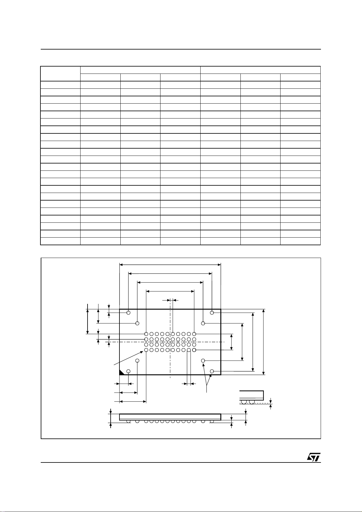
M58MR064C, M58MR064D
Table 38. TFBGA48 - 10 x 4 ball array, 0.5 mm pitch, Package Mech anical Data
Symbol
Typ Min Max Typ Min Max
A 0.950 1.200 0.0374 0.0472
A1 0.200 0.300 0.0079 0.0118
A2 0.790 0.0311
b 0.300 0.250 0.350 0.0118 0.0098 0.0138
D 10.530 10.480 10.580 0.4146 0.4126 0.4165
D1 4.500 – – 0.1772 – –
D2 6.500 – – 0.2559 – –
D3 8.500 – – 0.3346 – –
ddd 0.080 0.0031
E 6.290 6.240 6.340 0.2476 0.2457 0.2496
E1 1.500 – – 0.0591 – –
E2 3.500 – – 0.1378 – –
E3 5.500 – – 0.2165 – –
e 0.500 – – 0.0197 – –
FD 3.015 – – 0.1187 – –
FD1 2.015 – – 0.0793 – –
FD2 1.015 – – 0.0400 – –
FE 2.395 – – 0.0943 – –
FE1 1.395 – – 0.0549 – –
FE2 0.395 – – 0.0156 – –
SD 0.250 – – 0.0098 – –
SE 0.250 – – 0.0098 – –
millimeters inches
Figure 21. TFBGA48 - 10 x 4 ball array, 0.5 mm pitch, Bo t tom View Package Outline
D
D3
D2
D1
FE
Drawing is not to scale.
FE1 FE2
e
SE
BALL "A1"
FD2
FD1
FD
A
SD
b
DUMMY BALLS
A1
E1
A2
E2
E3
E
ddd
BGA-Z17
50/52

M58MR064C, M58MR064D
Figure 22. TFBGA48 Daisy Chain - Package Connections (Top view through package)
12 78 13121110914
A
B
C
D
E
F
G
H
6543
Figure 23. TFBGA48 Daisy Chain - PCB Connections proposal (Top view through package)
12 78 13121110914
A
B
START
C
D
E
F
G
H
POINT
6543
END
POINT
AI90107
AI90108
51/52

M58MR064C, M58MR064D
Information furnished is believed to be accurate and reliable. However, STMicroelectronics assumes no responsibility for the consequences
of use ofsuch information nor for any infringement of patents or other rights of third parties which mayresult from its use. No license isgranted
by implication or otherwise under any patent or patent rights of STMicroelectronics. Specifications mentioned in this publication are subject
to change without notice. This publication supersedes and replaces all information previously supplied. STMicroelectronics products are not
authorized for use as critical components in life support devices or systems without express written approval of STMicroelectronics.
The ST logo is registered trademark of STMicroelectronics
All other names are the property of their respective owners.
2002 STMicroelectronics - All Rights Reserved
Australia - Brazil - China - Finland - France - Germany - Hong Kong - India - Italy - Japan - Malaysia - Malta - Morocco -
Singapore - Spain - Sweden - Switzerland - United Kingdom - U.S.A.
STMicroelectronics GROUP OF COMPANIES
www.st.com
52/52
 Loading...