

32 Mbit (2Mb x16, Mux I/O, Dual Bank, Burst)
■ SUPPLY VOLTAGE
= V
–V
DD
Erase and Read
–V
= 12V for fast Program (optional)
PP
■ MULTIPLEXED ADDRESS/DATA
■ SYNCHRONOUS / ASYNCHRONOUS READ
– Burst mode Read: 40MHz
– Page mode Read (4 Words Page)
– Random Access: 100ns
■ PROGRAMMING TIME
– 10µs by Word typical
– Two or four words programming option
■ MEMORY BLOCKS
– Dual Bank Memory Array: 8/24 Mbit
– Parameter Blocks (Top or Bott o m location)
■ DUAL OPERATIONS
– Read within one Bank while Program or
Erase within the other
– No delay between Read and Write operations
■ PROTECTION/S ECURITY
– All Blocks protected at Power-up
– Any combination of Blocks can be protected
– 64 bit unique device identifier
– 64 bit user programmable OTP cells
– One parameter block permanently lockable
■ COMMON FLASH INTERFACE (CFI)
■ 100,000 PROGRAM/ERASE CYCL ES per
BLOCK
■ ELECTRONIC SIGNATURE
– Manufacturer Code: 20h
– Top Device Code, M58MR032C: 88DAh
– Bottom Device Code, M58MR032D: 88DBh
= 1.7V to 2.0V for Program,
DDQ
M58MR032C
M58MR032D
1.8V Supply Flash Memory
PRELIMINARY DATA
FBGA
TFBGA48 (ZC)
10 x 4 ball array
Figure 1. Logic Diagram
V
V
DDQVPP
DD
A16-A20
W
RP
WP
5
E
G
L
K
M58MR032C
M58MR032D
V
SS
16
ADQ0-ADQ15
WAIT
BINV
AI90019
August 2002
This is preliminary information on a new product now in development or undergoing evaluation. Details are subject to change without notice.
1/52
M58MR032C, M58MR032D
Figure 2. TFBGA Connections (Top view through package)
87654321
A
B
C
D
E
F
G
H
DU
DU
DU
DU
DDQ
SS
NC
V
ADQ14ADQ15
SS
SS
KWAIT
ADQ13 ADQ12
DD
WV
WPRPBINVLA20A16V
ADQ2ADQ3ADQ6ADQ7V
ADQ10ADQ11ADQ4ADQ5V
V
109
A19
A18
DDQ
A17
ADQ8
ADQ1
PP
ADQ9
V
1211
DU
NC
V
E
SS
G
ADQ0
DU
1413
DU
DU
AI90020
DESCRIPTION
The M58MR032 is a 32 Mbit non-volatile Flash
memory that m ay be erased electrically a t block
level and programmed i n-system on a Word-byWord basis using a 1.7V to 2.0V V
supply for the
DD
circuitry. For Program and Erase operations the
necessary high voltages are gen erated internally.
The device supports synchronous burst read and
asynchronous read from all the blocks of the memory array; at power-up the device is configured for
page mode read. In sy nchronous burst mode, a
new data is output at each clock cycle for frequencies up to 40MHz.
The array matrix organization allows each block to
be erased and reprogrammed without affecting
other blocks. All blocks are protected against programming and erase at Power-up.
Blocks can be unprotected to make changes in the
application and then re-protected.
A parameter block "Security block" can be permanently protected against programming and erasing
2/52
in order to increase the data security. An optional
12V V
power supply is provided to speed up the
PP
program phase at costumer production. An internal command interface (C.I.) decode s the instructions to access/modify the memory content. The
program/erase controller (P/E.C.) automatically
executes the algorithms taking care of the timings
necessary for program and erase operations. Two
status registers indicate the state of each bank.
Instructions for Read Array, Read Electronic Signature, Read Status Register, Clear Status Register, Write Read Configuration Register, Program,
Block Erase, Bank Erase, Program Suspend, Program Resume, Erase Suspend, Erase Resume,
Block Protect, Block Unprotect, Block Locking,
Protection Program, CFI Query, are wri tten to t he
memory through a Command Interface (C.I.) using
standard micro-processor write timings.
The memory is offered in TFBGA48, 0. 5 mm ball
pitch packages and it is supplied with all the bits
erased (set to ’1’).
M58MR032C, M58MR032D
Table 1. Signal Names
A16-A20 Address Inputs
ADQ0-ADQ15
Data Input/Outputs or Address
Inputs, Command Inputs
Organization
The M58MR032 is organized as 2Mb by 16 bits.
The first sixteen address lines are multiplexed with
the Data Input/Output signals on the m ultiplexed
address/data bus ADQ0-ADQ15. The remaining
address lines A16-A20 are the MSB addresses.
E
G
W
RP
Chip Enable
Output Enable
Write Enable
Reset/Power-down
Chip Enable E
W
inputs provide memory control.
, Output Enable G and Write Enable
The clock K input synchronizes the memory to the
microprocessor during burst read.
Reset RP
is used to reset all the memory circuitry
and to set the chip in power-down mode if a proper
setting of the Read Configuration Register en-
WP
K Burst Clock
L
Write Protect
Latch Enable
ables this function.
output indicates to t he microprocessor the
WAIT
status of the memory during the burst mode operations.
Memory Blocks
WAIT
BINV Bus Invert
V
DD
V
DDQ
V
PP
Wait Data in Burst Mode
Supply Voltage
Supply Voltage for Input/Output
Buffers
Optional Supply Voltage for
Fast Program & Erase
The device features asymmetrically blocked architecture. M58MR032 has an array of 71 blocks and
is divided into two banks A and B, prov iding D ual
Bank operations. While programming or erasing in
Bank A, read operations are possible into Bank B
or vice versa. Only one bank at the time is allowed
to be in program or erase mode. It is possible to
perform burst reads that cross bank boundaries.
The memory features an eras e suspend allowing
reading or programming in another block. Once
suspended the erase can be resumed. Program
V
SS
Ground
can be suspended to read data in another block
and then resumed. The Bank S ize and sectoriza-
DU Don’t Use as Internally Connected
NC Not Connected Internally
tion are summarized in Table 3. Parameter Blocks
are located at the top of the memory address
space for the M58MR032C, and at the bottom for
the M58MR032D. The memory maps are shown in
Figure 3.
Table 2. Absolute Maximum Ratings
Symbol Parameter Value Unit
T
A
T
BIAS
T
STG
(3)
V
IO
, V
V
DD
DDQ
V
PP
Note: 1. Except for the ratin g "Operati ng Temperature Range" , stresses above those listed i n t he Table "Absolute M aximum Ratings" may
cause permanent damage to the device. These are stress ratings only and operation of the device at these or any other conditions
above those indi cated in t he Operating sect i ons of thi s specifi cation i s not impl i ed. Exposure to Absolute M aximum Rating c onditions for extended per iods may aff ect device reliabilit y. Refer also to the STMicroel ectronics SURE Program an d other relevan t qual ity docum en ts .
2. Depends on range.
3. Mini m um Voltage may undershoot to –2V duri ng transit i on and for less than 20ns.
Ambient Operating Temperature
Temperature Under Bias –40 to 125 °C
Storage Temperature –55 to 155 °C
Input or Output Voltage
Supply Voltage –0.5 to 2.7 V
Program Voltage –0.5 to 13 V
(1)
(2)
–40 to 85 °C
–0.5 to V
DDQ
+0.5
V
3/52
M58MR032C, M58MR032D
The architecture includes a 128 bits Protection
register that is divided into two 64-bits segments.
In the first one is written a unique device nu mbe r,
while the second o ne is programmable by the us er. The user programmable segm ent can be permanently protected programming the bit 1 of the
Protection Lock Register (see protection register
and Security Block). The parameter bl ock (# 0) is
a security block. It c an be permanently p rotected
Table 3. Bank Size and Sectorization
Bank Size Parameter Blocks Main Blocks
Bank A 8 Mbit 8 blocks of 4 KWord 15 blocks of 32 KWord
Bank B 24 Mbit - 48 blocks of 32 KWord
Figure 3. Me m ory Map
Top Boot Block
Address lines A20-A0
000000h
007FFFh
Bank B
512 Kbit or
32 KWord
Total of 48
Main Blocks
by the user programming the bit 2 of the Protection
Lock Register.
Block protection against Program or Erase provides additional data security. All blocks are protected and unlocked at Power-up. Instructions are
provided to protect or un-protec t any block in the
application. A second register locks the protection
status while WP
is low (see Block Locking descrip-
tion).
Bottom Boot Block
Address lines A20-A0
000000h
000FFFh
64 Kbit or
4 KWord
Total of 8
Parameter
Blocks
Bank A
178000h
17FFFFh
180000h
187FFFh
1F0000h
1F7FFFh
1F8000h
1F8FFFh
1FF000h
1FFFFFh
512 Kbit or
32 KWord
512 Kbit or
32 KWord
512 Kbit or
32 KWord
64 Kbit or
4 KWord
64 Kbit or
4 KWord
Total of 15
Main Blocks
Total of 8
Parameter
Blocks
Bank A
Bank B
007000h
007FFFh
008000h
00FFFFh
078000h
07FFFFh
080000h
087FFFh
1F8000h
1FFFFFh
64 Kbit or
4 KWord
512 Kbit or
32 KWord
Total of 15
Main Blocks
512 Kbit or
32 KWord
512 Kbit or
32 KWord
Total of 48
Main Blocks
512 Kbit or
32 KWord
AI90069
4/52

M58MR032C, M58MR032D
SIGNAL DESCRIPTIONS
See Figure 1 and Table 1.
Address Inputs or Data Input/Output (ADQ0ADQ15). When Chip Enable E
put Enable G
is at VIH the multiplexe d address/
is at VIL and Out-
data bus is used to input addresses for the memory array, data to be programmed in the memory array or commands to be written to the C.I. The
address inputs for the memory array are latched
on the rising edge of Latch Enable L
latch is transparent when L
is at VIL. In synchro-
. The address
nous operations the address is also latched on the
first rising/falling edge of K (depending on clock
configuration) when L
is low. Both input data and
commands are latched on the rising edge of Write
Enable W
able G
. When Chip Ena ble E and Output En-
are at VIL the address/data bus outputs
data from the Memory Array, the Electronic Signature Manufacturer or Device codes, the Block Protection status the Read Configuration Register
status, the protection register or the Status Register. The address/data bus is high impedance when
the chip is desele cted, O ut put E nabl e G
is at VIL.
or RP
is at VIH,
Address Inputs (A16-A20). The five MSB addresses of the m emory array are latched on t he
rising edge of Latch Enable L
. In synchronous operation these inputs are also latched on the first
rising/falling edge of K (depending on clock configuration) when L
Chip Enable (E
is low.
). The Chip Enable input activates the memory control logic, input buffers, decoders and sense amplifiers. E
at VIH deselects
the memory and red uces the power consumption
to the standby level. E
can also be used to control
writing to the command register and to the memory array, while W
Output Enable (G
remains at VIL.
). The Output Enable gates the
outputs through the data buffers during a read operation. When G
is at VIH the outputs are High im-
pedance.
Write Enable (W
). This input controls writing to
the Command Register and Data latches. Data are
latched on the rising edge of W
Write Protect (WP
). This input gives an addition-
.
al hardware protection level against program or
erase when pulled at V
, as described in the Block
IL
Lock instruction description.
Reset/Power-down Input (RP
). The RP input
provides hardware reset of the memory, and/or
Power-down functions, depending on the Read
Configuration Register status. Reset /Po wer-down
of the memory is achieved by pulling RP
to VIL for
at least t
. When the reset pulse is given, the
PLPH
memory will recover from Power-down (when enabled) in a minimum of t
PHEL
, t
PHLL
or t
PHWL
(see
Table 31 and F igure 15) after the rising edge of
. Exit from Reset/Power-down changes the
RP
contents of the Read Configuration Register bits
14 and 15, setting the mem ory in asynchronous
page mode read and power save function disabled. All blocks are protected and unl oc ked after
a Reset/Power-down.
Latch Enable (L
). L latches the address bits
ADQ0-ADQ15 and A16-A20 on its rising edge.
The address latch is transparent when L
is at V
and it is inhibited when L is at VIH.
Clo c k (K). The clock input synchronizes the
memory to the micro controller during burst mode
read operation; the address is latched on a K edge
(rising or falling, according to the configuration settings) when L
is at VIL. K is don’t care during asyn-
chronous page mode read and in write operations.
Wait (WAIT
). WAIT i s an output signal used dur-
ing burst mode read, indicating whet her the data
on the output bus are valid or a wait state must be
inserted. This output is high impedance when E
are high or RP is at VIL, and can be configured
G
or
to be active during the wait cycle or one clock cycle in advance.
Bus Invert (BINV). BINV is an input/output signal
used to reduce the amount of power needed to
switch the external address/data bus. The power
saving is achieved by inverting the dat a output on
ADQ0-ADQ15 every time this gives an advantage
in terms of number of toggling bits. In burst mode
read, each new data output from the memory is
compared with the previous data. If the number of
transitions required on the data bus is in excess of
8, the data is inverted and the BINV signal will be
driven by the memory at V
to inform the receiv-
OH
ing system that dat a must be inverted b efore any
further processing. By doing so, the act ual transitions on the data bus will be less than 8.
In a similar way, when a command is given, BINV
may be driven by the system at V
to inform the
IH
memory that the data input must be inverted.
Like the other input/output pins, BINV is high im-
pedance when the chip is deselected, output enable G
is at VIH or RP is at VIL; when used as an
input, BINV must follow the same set-up and h old
timings of the data inputs.
and V
V
DD
is the main power supply for all operations
V
DD
(Read, Program and Erase). V
Supply Voltage (1.7V to 2.0V).
DDQ
is the supply
DDQ
voltage for Input and Output.
IL
5/52

M58MR032C, M58MR032D
VPP Program Supply Voltage (12V). VPP is both
a control input and a po wer supply pin. The two
functions are selected by the voltage range applied to the pin; if V
(0 to 2V) V
is seen as a control inpu t, and the
PP
is kept in a low voltage range
PP
current absorption is limited to 5µA (0.2µA typical).
In this ca se wi th V
protection against program or erase; with V
V
these functions are enabled (see T able 26).
PP1
V
value is only sampled during program or
PP
= VIL we obtain an absolute
PP
PP
=
erase write cycles; a chang e in its v alue after t he
operation has been started does not have any effect and program or erase are carried on regularly.
If V
is used in the 11.4V to 12.6V range (V
PP
PPH
then the pin acts as a power supply (see Table
26). This supply voltage must remain stable as
long as program or erase are running. In read
mode the current sunk is less then 0.5mA, while
during program and erase operations the current
may increase up to 10mA.
Ground. VSS is the reference for al l the vol t-
V
SS
age measurements.
)
6/52
M58MR032C, M58MR032D
DEVICE OPERATIONS
The following operations can be performed using
the appropriate bus cycle s: Address Latch, Read
Array (Random, and Page Modes), Write command, Output Disable, Standby, reset/Powerdown and Block Locking. See Table 4.
Address Latch. In asynchronous operation, the
address is latched on the rising edge of L
input. In
burst mode the address is latched either on the rising edge of L
(depending on configuration settings) when L
or on the first rising/falling edge of K
is
low.
Read. Read operations are used to output the
contents of the Memory Array, the Electronic Sig-
Table 4. User Bus Operations
(1)
nature, the Status Register, the CFI, the Block
Protection Status, the Read Configuration Register status and the Protection Register.
Read operation of the Memory Array may be performed in asynchronous page mode or synchronous burst mode. In asynchronous page mode
data is internally read and stored in a page buffer.
The page has a size of 4 words and is addres sed
by ADQ0 and ADQ1 address inputs.
According to the device configuration the following
Read operations: Electronic Signature - Status
Register - CFI - Block Protection Status - Read
Configuration Register Status - Protection Register must be accessed as asynchronous read or as
single synchronous read (see Figure 4).
Operation E G W L RP WP ADQ15-ADQ0
V
Address Latch
Write
Output Disable
Standby
V
IL
V
IL
V
IL
V
IH
V
IH
V
IH
V
IH
V
IH
V
IL
V
IH
(rising edge)
XX X
Reset / Power-down X X X X
Block Locking
Note: 1. X = Don’t care.
V
IL
XX X
IL
V
IH
V
IH
V
IH
V
IH
V
IH
V
IH
V
IL
V
IH
V
IH
V
IH
V
IH
X
X
V
IL
Address Input
Data Input
Hi-Z
Hi-Z
Hi-Z
X
(3)
(1)
ADQ0
Table 5. Read Electronic Signature (AS and Read CFI instructions)
Code Device E
Manufacturer Code
M58MR032C
V
IL
V
IL
G W
V
IL
V
IL
ADQ1
V
IH
V
IH
V
IL
V
IL
Device Code
M58MR032D
Note: 1. Addresses are latch ed on the risin g edge of L i nput.
2. EA means Electronic Signature Address (see Read Electronic Signature)
3. Value during address latch.
V
IL
Table 6. Read Block Protection (AS and Read CFI instructions)
Block Status E
Protected and unlocked
Unprotected and unlocked
Protected and locked
Unprotected and locked
Note: 1. Addresses are latch ed on the risin g edge of L i nput.
2. A locked block ca n be unprotec ted only with WP
3. Value during address latch.
4. BA means Block Address. Fir st cy cle command address should indicat e the bank of the block address.
(2)
V
IL
V
IL
V
IL
V
IL
V
IL
G W
V
IL
V
IL
V
IL
V
IL
at V
IH.
V
IH
V
IH
V
IH
V
IH
V
IH
V
IL
ADQ1
V
IH
V
IH
V
IH
V
IH
(3)
(1)
ADQ0
(3)
Address
V
IL
V
IH
V
IH
(3)
V
IL
V
IL
V
IL
V
IL BA
Other
(2)
EA
(2)
EA
(2)
EA
Other
Address
(4)
BA
(4)
BA
(4)
BA
(4)
(2)
ADQ15-0
0020h
88DAh
88DBh
ADQ15-0
0001
0000
0003
0002
7/52
M58MR032C, M58MR032D
Table 7. Read Protection Register (RSIG and RCFI Instruction)
(1)
Word E G W A20-17 ADQ15-8 ADQ7-0 ADQ15-8 ADQ7-3 ADQ2 ADQ1 ADQ0
Lock
Unique
ID 0
Unique
ID 1
Unique
ID 2
Unique
ID 3
OTP 0
OTP 1
OTP 2
OTP 3
Note: 1. Addresses are latch ed on the ri si ng edge of L i nput.
V
ILVILVIH
V
ILVILVIH
V
ILVILVIH
V
ILVILVIH
V
ILVILVIH
V
ILVILVIH
V
ILVILVIH
V
ILVILVIH
V
ILVILVIH
2. X = Don’t ca re.
X
X
X
X
X
X
X
X
X
(2)
(2)
(2)
(2)
(2)
(2)
(2)
(2)
(2)
X
X
X
X
X
X
X
X
X
(2)
(2)
(2)
(2)
(2)
(2)
(2)
(2)
(2)
80h 00h 00000B
Security
prot.data
81h ID data ID data ID data ID data ID data
82h ID data ID data ID data ID data ID data
83h ID data ID data ID data ID data ID data
84h ID data ID data ID data ID data ID data
85h OTP data
86h OTP data
87h OTP data
88h OTP data
OTP
data
OTP
data
OTP
data
OTP
data
OTP
data
OTP
data
OTP
data
OTP
data
OTP
prot.data
OTP
data
OTP
data
OTP
data
OTP
data
0
OTP
data
OTP
data
OTP
data
OTP
data
Table 8. Dual Bank Operations
(1, 2, 3)
Commands allowed in the other bank
Status of one
bank
Read
Array
Read
Status
Read
ID/CFI
Program
Erase/
Erase
Resume
Program
Suspend
Erase
Suspend
Protect
Unprotect
Idle Yes Yes Yes Yes Yes Yes Yes Yes
Reading ––––––––
Programming Yes Yes Yes – – – – Yes
Erasing Yes Yes Yes – – – – Yes
Program
Suspended
Erase
Suspended
Note: 1. For detailed description of command see Table 33 and 34.
2. Ther e i s a status register for each bank; status register indicates bank state, no t P /E . C. status.
3. Command must be written to a n address within the bl ock targeted by that com m and.
Yes Yes Yes – – – – Yes
Yes Yes Yes Yes – Yes – Yes
8/52
M58MR032C, M58MR032D
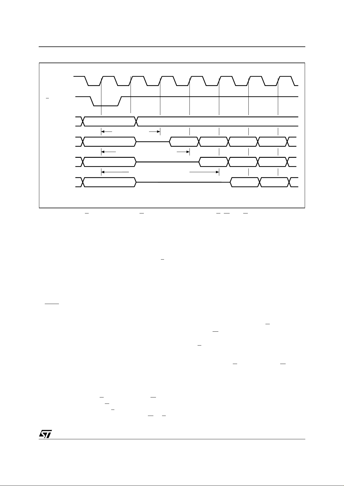
Figure 4. Single Synchronous Read Sequence (RSIG, RCFI, RSR instructions)
K
L
A20-A16
ADQ15-ADQ0
ADQ15-ADQ0
ADQ15-ADQ0
VALID ADDRESS
CONF. CODE 2
VALID ADDRESS VALID DATA NOT VALID
CONFIGURATION CODE 3
VALID ADDRESS VALID DATA
CONFIGURATION CODE 4
VALID ADDRESS NOT VALID
Both Chip Enable E and Output Enable G must be
at V
in order to read the output of the memory.
IL
Read array is the default state of the device when
exiting power down or after power up.
Burst Read. The device also supports a burst
read. In this mode a burst sequence is s tarted at
the first clock edge (risin g or falling according to
configuration settings) after th e falling edge of L
After a configurable delay of 2 to 5 clock cycles a
new data is output at each clock cycle. The burst
sequence may be configured for linear or interleaved order and for a length of 4, 8 words or for
continuous burst mode. Wrap and no-wrap modes
are also supported.
A WAIT
signal may be asserted to indicate to the
system that an output delay will occur. This delay
will depend on the starting address of the burst sequence; the worst case dela y will o ccur w hen the
sequence is crossing a 64 word boundary and the
starting address was at the end of a four word
boundary. See the Write Read Configuration Register (CR) Instruction for more details on all the
possible settings for the synchronous burst read
(see Table 14). It is possible to perform burst read
across bank boundary (all banks in read array
mode).
Write. Write operations are used to give I nstruction Commands to the memory or to latch Input
Data to be programmed. A write operation is initiated when Chip Enable E
at V
with Output Enable G at VIH. Addresses are
IL
latched on the rising edge of L
put Data are latched on the rising edge of W
and Write Enable W are
. Commands and In-
or E
whichever occurs first. Noise pulses of less than
5ns typical on E
NOT VALID
NOT VALID
VALID DATA
, W and G signals do not start a
NOT VALID
NOT VALID
write cycle. Write operations are asynchronous
and clock is ignored during write.
Dual Bank Operations. The Dual Bank allows to
run different operations simultaneously i n the tw o
banks. It is possible to read array data from one
bank while the other is programming, erasing or
reading any data (CFI, status register or electronic
.
signature).
Read and write cycles can be initiated for simulta-
neous operations in different banks without any
delay. Only one b ank at a time is all owed to be in
program or erase mode, while the other must be in
one of the read modes (see Table 8).
Commands must be writt en to an address within
the block targeted by that command.
Output Disa bl e . The data outputs are high impedance when the Output Enable G
Write Enable W
at VIH.
is at VIH with
Standby. The mem ory is in standby when C hip
Enable E
is at VIH and the P/E.C. is idle. The power consumption is reduced to the standby level
and the outputs are high impedance, independent
of the Output Enable G
or Write Enable W inputs.
Automatic Standby. When in Read mode, after
150ns of bus inactivity and when CMOS levels are
driving the addresses, the chip automatically enters a pseudo-standby mode where consumption
is reduced to the CMOS standby value, while outputs still drive the bus. The automatic standby feature is not available when the device is configured
for synchronous burst mode.
AI90022
9/52
M58MR032C, M58MR032D
Table 9. Identifier Codes
Code Address (h) Data (h)
Manufacturer Code Bank Address + 00 0020
Device Code
Block Protection
Die Revision Code Bank Address + 03
Read Configuration Register Bank Address + 05
Lock Protection Register Bank Address + 80
Protection Register
Note: 1. DRC means Die Revisio n Co de.
CR means Read Configuration Register.
LPR means Lock Protection Register.
PR means Uni q ue Device Number and User Progra mmable OTP.
Reset/Power-down. The memory is in Powerdown when the Read Configuration Register is set
for Power-down and RP
sumption is reduced to the Power-down level, and
Outputs are in high impedance, independent of the
Chip Enable E
W
inputs. The memory is in reset when the Read
, Output Enabl e G or Write Enab le
Configuration Register is set for Reset and RP
at VIL
. The power consumption is the same of the
standby and the outputs are in hig h impedance.
After a Reset/Power down t he device defaults to
Top Bank Address + 01 88DA
Bottom Bank Address + 01 88DB
Protected and Unlocked
Unprotected and Unlocked 0000
Protected and Locked 0003
Unprotected and Locked 0002
Bank Address + 02
Bank Address + 81
Bank Address + 88
Block Locking. Any combination of blocks can
be temporarily protected against Program or
is at VIL. The power con-
Erase by setting the lock register and pulling WP
to VIL. The following summarizes the locking operation. All blocks are protected on power-up. They
can then be unprotected or protected with the Unprotect and Protect commands. The Lock com-
is
mand protects a b lock and prev ents it from being
unlocked when WP
overridden. Lock is cleared only when the dev ice
is reset or powered-down (see Protect instruction).
read array mode, the status register is set to 80h
and the read configuration register defaults to
asynchronous read.
0001
(1)
DRC
(1)
CR
(1)
LPR
(1)
PR
= 0. When WP = 1, Lock is
10/52
M58MR032C, M58MR032D
INSTRUCTIONS AND COMMANDS
Eighteen instructions are available (see Tables 10
and 11) to perform Read Memory Array, Read Status Register, Read Electronic Signature, CFI Query, Block Erase, Bank Erase, Program, Tetra Word
Program, Double Word Program, Clear Status
Register, Program/Erase Suspend, Program/
Erase Resume, Block Protect, Block Unprotect,
Block Lock, Protection Register Program, Read
Configuration Register and Lock Protection Program.
Status Register ou tput may be read at any time,
during programming or erase, to monitor the
progress of the operation.
An internal Command Interface (C.I.) decodes the
instructions while an internal Program/Erase Controller (P/E.C.) handles all timing and verifies the
correct execution of the Program and Erase instructions. P/E.C. provides a Status Register
whose bits indicate operation and exit status of the
internal algorithms. The Command Interface is reset to Read Array when power is first applied,
when exiting from Reset or whenever V
than V
. Command sequence must be followed
LKO
is lowe r
DD
exactly. Any invalid combination of commands will
reset the device to Read Array.
Read (RD)
The Read instruction consists of o ne write cycle
(refer to Device Operations section) and places
the addressed bank in Read Array mode. When a
device reset occurs, the memo ry is in Read Array
as default. A read array command will be ignored
while a bank is programming or erasing. However
in the other bank a read array command will be accepted.
Read Status Register (RSR)
A bank’s Status Register indicates when a program or erase operation is complete and the success or failure of operation itself. Issue a Read
Status Register Instruction (70h) to read the Status Register content of t he addressed bank. The
status of the other bank is not affected by the command. The Read S tatus Register instruction may
be issued at any time, also when a Program/Erase
operation is ongoing. T he following Read operations output the content of the Status Register of
the addressed bank. The Status Register is
latched on th e fa lling edg e of E
can be read until E
must be toggled to update the latched data.
G
or G returns to VIH. Either E or
or G signals, and
Read Electronic Signature (RSIG)
The Read Electronic Signature instruction consists of one write cycle (refer to Device Operations
section) giving the com mand 90h to an address
Table 10. Commands
Hex Code Command
00h Invalid Reset
01h Protect Confirm
03h
10h Alterna tive Program Set-up
20h Block Erase Set-up
2Fh Lock Confirm
30h Double Word Program Set-up
40h Program Set-up
50h Clear Status Register
55h Tetra Word Program Set-up
60h
70h Read Status Register
80h Bank Erase Set-up
90h Read Electronic Signature
98h CFI Query
B0h Program/Erase Suspend
C0h
D0h
FFh Read Array
Write Read Configuration Register
Confirm
Protect Set-up and Write Read
Configuration Register
Protection Program and Lock Protection
Program
Program/Erase Resume, Erase Confirm
or Unprotect Confirm
within the bank A. A subsequent read in the ad-
dress of bank A will output the Manufacturer Code,
the Device Code, the protection Status of Blocks
of bank A, the Die Revision Code, the Protect ion
Register, or the Read Configuration Register (see
Table 9).
If the first write cycle of Read Electronic Signature
instruction is issued to an address within the bank
B, a subsequent read in an address of bank B will
output the protection Status of Blocks of bank B.
The status of the other bank is not affected by the
command (see Table 8).
See Tables 5, 6, 7 and 8 for the valid address. The
Electronic Signature can be read from the memory
allowing programming equipment or applications
to automatically match their interface to the char-
acteristics of M58MR032C and M58MR032D.
11/52
M58MR032C, M58MR032D
Table 11. Instructions
Instruction Cyc. Ope ration
Read
RD
Memory
1+ Write BKA FFh
Array
RSR
Read Status
Register
1+ Write BKA 70h
Read
READ
RSIG
Electronic
1+ Write EA 90h
Signature
RCFI Read CFI 1+ Write CA 98h
CLRS
(5)
Register
1 Write BKA 50h
Clear Status
EE Block Erase 2 Write BA 20h Write BA D0h
BE Bank Erase 2 Write BKA 80h Write BKA D0h
PG Program 2 Write WA 40h or 10h Write WA WD
DPG
TPG
Double Word
Program
Tetra Word
Program
3 Write WA1 30h Write WA1 WD1
5 Write WA1 55h Write WA1 WD1
Address
(1,2)
Data
(3)
(1)
(1)
(1)
(1)
Address
(1,2)
Read
Address
BKA
EA ED
CA CD
Operation
Read
Read
Read
Read
Write WA2 WD2
Write WA2 WD2
(3)
Data
Data
Status
Register
Write WA3 WD3
PROGRAM/ERASE
Write WA4 WD4
Program
PES
Erase
1 Write BKA B0h
Suspend
Program
PER
Erase
1 Write BKA D0h
Resume
BP Block Protect 2 Write BA 60h Write BA 01h
Block
BU
Unprotect
PROTECT
BL Block Lock 2 Write BA 60h Write BA 2Fh
2 Write BA 60h Write BA D0h
Protection
PRP
Register
2 Write PA C0h Write PA PD
Program
Lock
LPRP
Protection
Register
2 Write LPA C0h Write LPA LPD
Program
CR
Write Read
Configuration
2 Write RCA 60h Write RCA 03h
CONFIGURATION
Register
12/52

M58MR032C, M58MR032D
Note: 1. First cycle command address should be the same as the operation’s target address. The first cycle of the RD, RSR, RSIG or RCFI
CFI Query (RCFI)
The CFI Query Mode is associated to bank A. The
address of the first write cycle must be within the
bank A. The status of the other bank is not affected
by the command (see Table 8). Writing 98h the device enters the Common Flash Interface Query
mode. Next read operations in the bank A will read
the CFI data. Write a read instruction to return to
Read mode (refer to the Common Flash Interface
section).
Clear Status Register (CLSR)
The Clear Status Register uses a single write operation, which resets bits b1, b3, b4 e b5 of the status register. The Clear Status Register is executed
writing the command 50h independently of the applied V
the device returns to read array mode. The Clear
Status Register command clears only the status
register of the addressed bank.
Block Erase (EE)
Block erasure sets all the bits within the selected
block to ’1’. One block at a time can be erased. It
is not necessary to pre-program the block as the
P/E.C. will do it automatically before erasing. This
instruction use two writes cycles. The first command written is the Block Era se S et up c om m and
20h. The second command is the Erase Confirm
command D0h. An address within the block to be
erased should be given to the memory during t he
two cycles command. If the second command given is not an erase con firm, the status register bits
b4 and b5 are set and the instruction aborts.
instruction is followed by read operations in the bank array or special register. Any number of read cycles can occur after one command cycle.
2. BKA m eans Address within the bank;
BA means Block Address;
EA means Elec tronic Signature Address;
CA means C om m on Flash Interface Address;
WA means Wo rd Address;
PA means Pr otection Register Ad dress (see Ta bl e 7);
LPA means Loc k Protection Register Address (see Table 7);
RCA means Read Configuration Register Ad dress.
3. PD means Protect i on Data;
CD means Common Flash Interface Data;
ED means Electronic Si gnature Data;
WD means Data to be prog rammed at t he address loc a t i on WA;
LPD means Lock protection Register Da ta
4. WA1, WA2, WA3 and WA 4 m ust be consecutive add ress differi ng only for address bits A1- A0.
5. Read cycle after e CLSR instruction will output the memory array.
After writing the command, the device outputs status register data when any address within the bank
is read. At the end of the operation the bank will remain in read status register until a read array command is written.
Status Register bit b7 is ’0’ while the erasure is in
progress and ’1’ when it has completed. After completion the Status Register bit b5 returns ’1’ if there
has been an Erase Failure. Status register b it b1
returns ’1’ if the user is attempting t o e rase a protected block. Status Register bit b3 returns a ’1’ if
is below V
V
PP
V
. As data integrity cannot be guaranteed when
IL
. Erase aborts if RP turns to
PPLK
the erase operation is aborte d, the eras e m ust be
repeated (see Table 1 2). A Clear Status Register
voltage. After executing this comm and
PP
instruction must be issued t o reset b1, b3, b4 and
b5 of the Status Register. During the execution of
the erase by the P/E.C., the bank with the block in
erase accepts only the RS R (Read St atus Register) and PES (Program/Erase Suspend) instructions. See figure 19 for Erase Flowchart and
Pseudo Code.
Bank Erase (BE)
Bank erase sets all the bits within the selected
bank to ’1’. It is not necessary to pre-program the
block as the P/E.C. will do it automatically before
erasing.
This instruction uses two writes cycles. The first
command written is the Bank Erase set-up command 80h. The second command is the Erase
Confirm command D0h. An address within the
bank to be erased should be given to the memory
during the two cycles command. See the Block
Erase command section for status register bit details .
13/52

M58MR032C, M58MR032D
Table 12. Status Register Bits
Mnemonic Bit Name
P/ECS 7 P/ECS
Status
ESS 6 Erase
Suspend
Status
Logic
Level
1 Ready Indicates the P/E.C. status, check during
0 Busy
1 Suspended
0
Definition Note
Program or Erase, and on completion before
checking bits b4 or b5 for Program or Erase
Success.
On an Erase Suspend instruction P/ECS and
In Progress or
Completed
ESS bits are set to ’1’. ESS bit remains ’1’ until
an Erase Resume instruction is given.
ES 5 Erase
PS 4 Program
VPPS 3 V
PSS 2 Program
BPS 1 Block
0 Reserved
Note: Logic level ’1’ is VIH and ’0’ is VIL.
Status
Status
Status
PP
Suspend
Status
Protection
Status
1 Erase Error ES bit is set to ’1’ if P/E.C. has applied the
0 Erase Success
1 Program Error
Program
0
Success
VPP Invalid,
1
Abort
V
0
1 Suspended
In Progress or
0
Completed
Program/Erase
1
on protected
Block, Abort
No operation to
0
protected blocks
Program (PG)
The Program instruction programs the array on a
word-by-word basis. The first command must be
given to the target block and only one partition can
be programmed at a time; the other partition must
be in one of the read m odes or in the erase sus pended mode (see Table 8).
This instruction uses two write cycles. The first
command written is the Program Set-up command
40h (or 10h). A second write operation latches the
Address and the Dat a to be writte n a nd starts the
P/E.C.
Read operations in the t argeted bank output the
Status Register content after the programming
has started.
The Status Register bit b7 returns ’ 0’ while the programming is in progress and ’1’ when it has completed. After completion the Status register bit b4
returns ’1’ if there has been a Program Failure (see
maximum number of erase pulses to the block
without achieving an erase verify.
PS bit set to ’1’ if the P/E.C. has failed to
program a word.
VPPS bit is set if the VPP voltage is below
V
when a Program or Erase instruction is
PPLK
PP
OK
executed. V
of the erase/program operation.
On a program Suspend instruction P/ECS and
PSS bits are set to ’1’. PSS remains ’1’ until a
Program Resume Instruction is given.
BPS bit is set to ’1’ if a Program or Erase
operation has been attempted on a protected
block.
is sampled only at the beginning
PP
Table 12). Status register bit b1 returns ’1’ if the
user is attempting to p rogram a protected block.
Status Register bit b3 returns a ’1’ if V
V
. Any attempt to write a ’1’ to an already pro-
PPLK
grammed bit will result in a program fail (status
register bit b4 set) if V
nored if V
PP
= V
PP1
PP
.
Programming aborts if RP
= V
goes to VIL. As data in-
and will be ig-
PPH
tegrity cannot be guaranteed when the program
operation is aborted, the block containing the
memory location must be erased and reprogrammed. A Clear Status Register instruction
must be issued to reset b5, b4, b3 and b1 of the
Status Register.
During the execution of the program by the P/E.C.,
the bank in prog ra mming accepts only the RSR
(Read Status Register) and PES (Program/Erase
Suspend) instructions. See Figure 16 for Program
Flowchart and Pseudo Code.
is below
PP
14/52
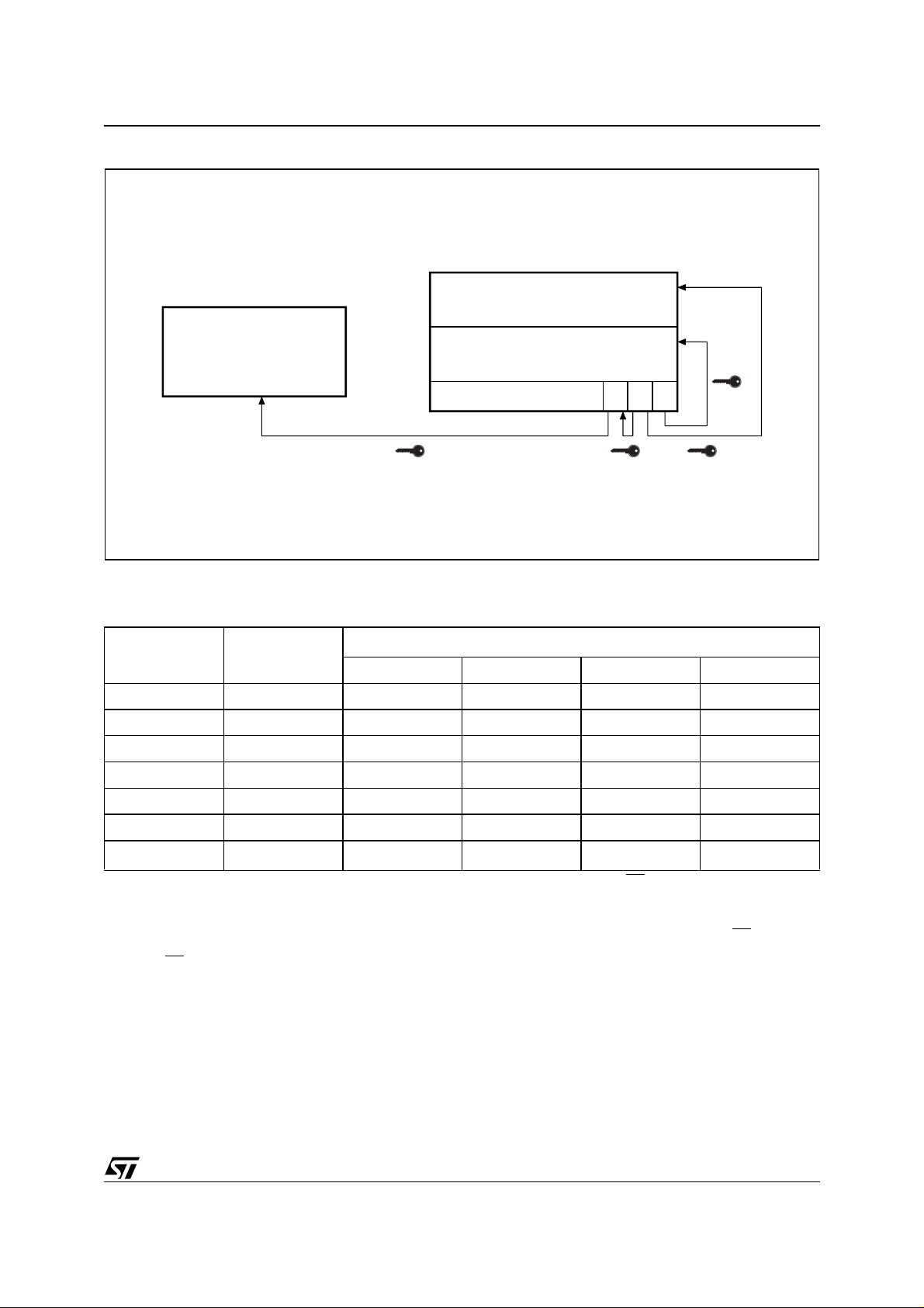
Figure 5. Security Block Memory Map
Parameter Block # 0
88h
85h
84h
81h
80h
M58MR032C, M58MR032D
User Programmable OTP
Unique device number
Protection Register Lock 2 1 0
AI90023
Table 13. Protection States
(2)
Current State
(WP, DQ1, DQ0)
Program/Erase
Allowed
(1)
Next State After Event
(3)
Protect Unprotect Lo ck WP transition
100 Yes 10 1 100 111 000
101 No 101 100 111 001
110 Yes 11 1 110 111 011
111 No 111 110 111 011
000 Yes 00 1 000 011 100
001 No 001 000 011 101
011 No 011 011 011
Note: 1. All blo cks are protected at power-up, so the default configuration i s 001 or 101 acc ording to WP status.
2. Current state and Next st at e gives the protection status of a block. Th e protecti on status is def i ned by the wr ite protec t i n and by
DQ1 (= 1 for a locked block) and DQ0 (= 1 for a protected block) as read in the Read Electronic Signature instruction with A1 = V
and A0 = VIL.
3. Next state is the protection status of a block after a Protect or Unprotect or Lock command has been issued or after WP
its logic value.
4. A WP
transition to VIH on a locked block will restore the previous DQ0 value, giving a 111 or 110.
111 or 110
(4)
IH
has changed
15/52

M58MR032C, M58MR032D
Doubl e Word Program (DP G)
This feature is offered to improve the programming
throughput, writing a page of two adjacent words
in parallel. The first command must be given to the
target block and only one partition can be programmed at a time ; the other p artition must be in
one of the read modes or in the erase suspended
mode (see Table 8).
The two words must differ only for the address A0.
Programming should not be attempted when V
is not at V
if V
is below V
PP
. The operation can also be executed
PPH
but result could be uncertain.
PPH
PP
These instructi on uses three write cycles. The first
command written is the Double Word Program
Set-Up command 30h. A second write operation
latches the Address and the Data of the first word
to be written, the third write operation latches the
Address and the Data of the second word to be
written and starts the P/E.C. (see Table 11).
Read operations in the t argeted bank output the
Status Register content after the programming
has started. The Status Register bit b7 ret urns ’0’
while the programming is in progress and ’1’ when
it has completed. After compl etion the S tatus register bit b4 returns ’1’ if there has been a Program
Failure. Status register bit b1 returns ’1’ if the user
is attempting to program a protected block. Status
Register bit b3 returns a ’1’ if V
is below V
PP
PPLK
Any attempt to write a ’1’ to an already programmed bit will result in a program fail (status
register bit b4 set). (See Table 12).
Programming aborts if RP
goes to VIL. As data integrity cannot be guaranteed when the program
operation is aborted, the memory location must be
erased and reprogrammed. A Clear Status Register instruction must be issued to reset b5, b4, b3
and b1 of the Status Register. During the execution of the program by the P/E.C., the bank in programming accepts only the RSR (Read Status
Register) instruction. See Figure 17 for Double
Word Program Flowchart and Pseudo code.
Tetra Word Program (TPG)
This feature is offered to improve the programming
throughput, writing a page of four adjacent words
in parallel. The first command must be given to the
target block and only one partition can be programmed at a time ; the other p artition must be in
one of the read modes or in the erase suspended
mode (see Table 8).
The four words must differ only for the addresses
A0 and A1. Programming should not be attempted
when V
is not at V
PP
be executed if V
PP
. The operation can also
PPH
is below V
but result could
PPH
be uncertain. These instruction uses five write cycles. The first comman d wri tten is t he Tetra Word
Program Set-Up command 55h. A second write
operation latches the Address and the Data of the
first word to be written, the third write operation
latches the Address an d the Data of the second
word to be written, the fourth write operation latches the Address and the Data of the third word to be
written, the fifth write operation latches the Address and the Data of the fourth word to be written
and starts the P/E.C. (see Table 11).
Read operations in the t argeted bank output the
Status Register content after the programming
has started. The Status Register bit b7 returns '0'
while the programming is in progress and '1' when
it has completed. After compl etion the S tatus register bit b4 returns '1' if there has been a Program
Failure. Status register bit b1 returns '1' if the user
is attempting to program a protected block. Status
Register bit b3 returns a '1' if V
is below V
PP
Any attempt to write a ’1’ to an already programmed bit will result in a program fail (status
register bit b4 set). (See Table 12).
Programming aborts if RP
goes to VIL. As data integrity cannot be guaranteed when the program
operation is aborted, the memory location must be
erased and reprogrammed. A Clear Status Register instruction must be issued to reset b5, b4, b3
and b1 of the Status Register. During the execution of the program by the P/E.C., the bank in programming accepts only the RSR (Read Status
Register) instruction. See Figure 17 for Tetra Word
Program Flowchart and Pseudo code.
.
Erase Suspend/Resume (PES/PER)
The Erase Suspend freezes , af t er a ce rtain latency period (within 25us), the erase operation and allows read in another block within the targeted bank
or program in the other block.
This instruction uses one write cycle B0h and the
address should be within the bank with the block
in erase (see Table 11). The device continues to
output status register data after the erase suspend
is issued. The status register bi t b7 and bi t b 6 are
set to ’1’ then the erase op eration has been sus pended. Bit b6 is set to '0' in case the erase is completed or in progress (see Table 12).
The valid commands while erase is suspended
are: Program/Erase Resume, Program, Read
Memory Array, Read St atus Regi ster, Read E lectronic Signature, CFI Query, Bloc k Protect, Block
Unprotect and Block Lock. The user can protect
the Block being erased issuing the B lock Protect
or Block Lock commands.
During a block erase suspend, the device goes
into standby mode by taking E
to VIH, which reduces active current draw. Erase is aborted if RP
to V
.
IL
If an Erase Suspend instruction was previously executed, the erase operation may be res umed by
issuing the command D0h using an address within
the suspended bank. The status register bit b6 and
bit b7 are cleared when erase resumes an d read
PPLK
turns
.
16/52
 Loading...