

128 Mbit (8Mb x16 or 4Mb x32, Uniform Block, Burst)
FEATURES SUMMARY
■ WIDE DATA BUS for HIGH BANDWIDTH
– M58LW128A: x16
– M58LW128B: x16/x32
■ SUPPLY VOLTAGE
–V
–V
■ SYNCHRONOUS/ASYNCHRONOUS READ
– Synchronous Burst read
– Pipelined Synchronous Burst Read
– Asynchronous Random Read
– Asynchronous Address Latch Controlled
– Page Read
■ ACCESS TIME
– Synchronous Burst Read up to 66MHz
– Asynchronous Page Mode Read 150/25ns
– Random Read 150ns
■ PROGRAMMING TIME
– 16 Word or 8 Double-Word Write Buffer
–12µs Word effective programming time
■ 128 UNIFORM 64 KWord MEMORY BLOCKS
■ BLOCK PROTECTION/ UNPROTECTION
■ PROGRAM and ERASE SUSPEND
■ OTP SECURITY AREA
■ COMMON FLASH INTERFACE
■ 100,000 PROGRAM/ERASE CYCLES per
BLOCK
■ ELECTRONIC SIGNATURE
– Manufacturer Code: 0020h
– Device Code M58LW128A: 881 8h
– Device Code M58LW128B: 8819h
= 2.7 to 3.6V core supply voltage for Pro-
DD
gram, Erase and Read operations
= 1.8 to VDD for I/O B u ffers
DDQ
Read
M58LW128A
M58LW128B
3V Supply Flash Memories
PRELIMINARY DATA
Figure 1. Packages
TSOP56 (N)
14 x 20mm
TBGA
TBGA64 (ZA)
10 x 13mm
TBGA
TBGA80 (ZA)
10 x 13mm
February 2003
This is preliminary information on a new product now in development or undergoing evaluation. Details are subject to change without notice.
1/65

M58LW128A, M58LW128B
TABLE OF CONTENTS
SUMMARY DESCRIPTION. . . . . . . . . . . . . . . . . . . . . . . . . . . . . . . . . . . . . . . . . . . . . . . . . . . . . . . . . . . 6
Figure 2. Logic Diagram . . . . . . . . . . . . . . . . . . . . . . . . . . . . . . . . . . . . . . . . . . . . . . . . . . . . . . . . . 7
Table 1. Signal Names . . . . . . . . . . . . . . . . . . . . . . . . . . . . . . . . . . . . . . . . . . . . . . . . . . . . . . . . . . 7
Figure 3. TSOP56 Connections. . . . . . . . . . . . . . . . . . . . . . . . . . . . . . . . . . . . . . . . . . . . . . . . . . . . 8
Figure 4. TBGA64 Connections for M58LW1 28A (Top view through package) . . . . . . . . . . . . . . . 9
Figure 5. TBGA80 Connections for M58LW1 28B (Top view through package) . . . . . . . . . . . . . . 10
Figure 6. Block Addresses. . . . . . . . . . . . . . . . . . . . . . . . . . . . . . . . . . . . . . . . . . . . . . . . . . . . . . . 11
SIGNAL DESCRIPTIONS . . . . . . . . . . . . . . . . . . . . . . . . . . . . . . . . . . . . . . . . . . . . . . . . . . . . . . . . . . . 11
Address Inputs (A1-A23). . . . . . . . . . . . . . . . . . . . . . . . . . . . . . . . . . . . . . . . . . . . . . . . . . . . . . . . . 11
Data Inputs/Outputs (DQ0-DQ31 ). . . . . . . . . . . . . . . . . . . . . . . . . . . . . . . . . . . . . . . . . . . . . . . . . .11
Chip Enable (E). . . . . . . . . . . . . . . . . . . . . . . . . . . . . . . . . . . . . . . . . . . . . . . . . . . . . . . . . . . . . . . . 1 1
Output Enable (G). . . . . . . . . . . . . . . . . . . . . . . . . . . . . . . . . . . . . . . . . . . . . . . . . . . . . . . . . . . . . . 11
Write Enable (W). . . . . . . . . . . . . . . . . . . . . . . . . . . . . . . . . . . . . . . . . . . . . . . . . . . . . . . . . . . . . . . 12
Reset/Power-Down (RP). . . . . . . . . . . . . . . . . . . . . . . . . . . . . . . . . . . . . . . . . . . . . . . . . . . . . . . . . 12
Latch Enable (L). . . . . . . . . . . . . . . . . . . . . . . . . . . . . . . . . . . . . . . . . . . . . . . . . . . . . . . . . . . . . . . . 12
Clock (K).. . . . . . . . . . . . . . . . . . . . . . . . . . . . . . . . . . . . . . . . . . . . . . . . . . . . . . . . . . . . . . . . . . . . . 12
Burst Address Advance (B). . . . . . . . . . . . . . . . . . . . . . . . . . . . . . . . . . . . . . . . . . . . . . . . . . . . . . . 12
Valid Data Ready (R). . . . . . . . . . . . . . . . . . . . . . . . . . . . . . . . . . . . . . . . . . . . . . . . . . . . . . . . . . . . 12
Word Organization (WORD).. . . . . . . . . . . . . . . . . . . . . . . . . . . . . . . . . . . . . . . . . . . . . . . . . . . . . . 12
Ready/Busy (RB). . . . . . . . . . . . . . . . . . . . . . . . . . . . . . . . . . . . . . . . . . . . . . . . . . . . . . . . . . . . . . . 13
Program/Erase Enable (V
V
Supply Voltage. . . . . . . . . . . . . . . . . . . . . . . . . . . . . . . . . . . . . . . . . . . . . . . . . . . . . . . . . . . . . 13
DD
Input/Output Supply Voltage (V
Ground (V
Ground (V
). . . . . . . . . . . . . . . . . . . . . . . . . . . . . . . . . . . . . . . . . . . . . . . . . . . . . . . . . . . . . . . . . . 13
SS
). . . . . . . . . . . . . . . . . . . . . . . . . . . . . . . . . . . . . . . . . . . . . . . . . . . . . . . . . . . . . . . . . 13
SSQ
). . . . . . . . . . . . . . . . . . . . . . . . . . . . . . . . . . . . . . . . . . . . . . . . . . . . . . 13
PP
). . . . . . . . . . . . . . . . . . . . . . . . . . . . . . . . . . . . . . . . . . . . . . . . 13
DDQ
BUS OPERATIONS. . . . . . . . . . . . . . . . . . . . . . . . . . . . . . . . . . . . . . . . . . . . . . . . . . . . . . . . . . . . . . . . 14
Asynchronous Bus Operations . . . . . . . . . . . . . . . . . . . . . . . . . . . . . . . . . . . . . . . . . . . . . . . . . . 14
Asynchronous Bus Read. . . . . . . . . . . . . . . . . . . . . . . . . . . . . . . . . . . . . . . . . . . . . . . . . . . . . . . . . 14
Asynchronous Latch Controlled Bus Read . . . . . . . . . . . . . . . . . . . . . . . . . . . . . . . . . . . . . . . . . . . 14
Asynchronous Page Read. . . . . . . . . . . . . . . . . . . . . . . . . . . . . . . . . . . . . . . . . . . . . . . . . . . . . . . . 14
Asynchronous Bus Write . . . . . . . . . . . . . . . . . . . . . . . . . . . . . . . . . . . . . . . . . . . . . . . . . . . . . . . . . 1 4
Asynchronous Latch Controlled Bus Write . . . . . . . . . . . . . . . . . . . . . . . . . . . . . . . . . . . . . . . . . . . 14
Output Disable. . . . . . . . . . . . . . . . . . . . . . . . . . . . . . . . . . . . . . . . . . . . . . . . . . . . . . . . . . . . . . . . . 15
Standby . . . . . . . . . . . . . . . . . . . . . . . . . . . . . . . . . . . . . . . . . . . . . . . . . . . . . . . . . . . . . . . . . . . . . . 15
Power-Down.. . . . . . . . . . . . . . . . . . . . . . . . . . . . . . . . . . . . . . . . . . . . . . . . . . . . . . . . . . . . . . . . . . 15
Table 2. Asynchronous Bus Operations . . . . . . . . . . . . . . . . . . . . . . . . . . . . . . . . . . . . . . . . . . . . 15
Synchronous Bus Operations . . . . . . . . . . . . . . . . . . . . . . . . . . . . . . . . . . . . . . . . . . . . . . . . . . .16
Synchronous Burst Read. . . . . . . . . . . . . . . . . . . . . . . . . . . . . . . . . . . . . . . . . . . . . . . . . . . . . . . . . 16
Synchronous Pipelined Burst Read. . . . . . . . . . . . . . . . . . . . . . . . . . . . . . . . . . . . . . . . . . . . . . . . .16
Synchronous Burst Read Suspend . . . . . . . . . . . . . . . . . . . . . . . . . . . . . . . . . . . . . . . . . . . . . . . . . 16
Table 3. Synchronous Burst Read Bus Operations. . . . . . . . . . . . . . . . . . . . . . . . . . . . . . . . . . . . 17
2/65

M58LW128A, M58LW128B
Table 4. Address Latch Cycle for Optimum Pipelined Synchronous Burst Read . . . . . . . . . . . . . 17
Figure 7. Synchronous Burst Read Operation. . . . . . . . . . . . . . . . . . . . . . . . . . . . . . . . . . . . . . . . 18
Figure 8. Example Synchronous Pipelined Burst Read Operation . . . . . . . . . . . . . . . . . . . . . . . . 18
Figure 9. Example Burst Address Advance and Burst Abort operations. . . . . . . . . . . . . . . . . . . . 19
Burst Configuration Register. . . . . . . . . . . . . . . . . . . . . . . . . . . . . . . . . . . . . . . . . . . . . . . . . . . . 20
Read Select Bit (M15) . . . . . . . . . . . . . . . . . . . . . . . . . . . . . . . . . . . . . . . . . . . . . . . . . . . . . . . . . . . 20
X-Latency Bits (M14-M11). . . . . . . . . . . . . . . . . . . . . . . . . . . . . . . . . . . . . . . . . . . . . . . . . . . . . . . . 20
Y-Latency Bit (M9). . . . . . . . . . . . . . . . . . . . . . . . . . . . . . . . . . . . . . . . . . . . . . . . . . . . . . . . . . . . . . 20
Valid Data Ready Bit (M8). . . . . . . . . . . . . . . . . . . . . . . . . . . . . . . . . . . . . . . . . . . . . . . . . . . . . . . . 20
Burst Type Bit (M7).. . . . . . . . . . . . . . . . . . . . . . . . . . . . . . . . . . . . . . . . . . . . . . . . . . . . . . . . . . . . . 20
Valid Clock Edge Bit (M6).. . . . . . . . . . . . . . . . . . . . . . . . . . . . . . . . . . . . . . . . . . . . . . . . . . . . . . . . 20
Latch Enable Bit (M3) . . . . . . . . . . . . . . . . . . . . . . . . . . . . . . . . . . . . . . . . . . . . . . . . . . . . . . . . . . . 20
Burst Length Bit (M2-M0). . . . . . . . . . . . . . . . . . . . . . . . . . . . . . . . . . . . . . . . . . . . . . . . . . . . . . . . . 20
Table 5. Burst Configuration Register. . . . . . . . . . . . . . . . . . . . . . . . . . . . . . . . . . . . . . . . . . . . . . 21
Table 6. Burst Type Definition (x16 Bus Width). . . . . . . . . . . . . . . . . . . . . . . . . . . . . . . . . . . . . . . 22
Table 7. Burst Type Definition (x32 Bus Width). . . . . . . . . . . . . . . . . . . . . . . . . . . . . . . . . . . . . . . 22
Table 8. Burst Performance. . . . . . . . . . . . . . . . . . . . . . . . . . . . . . . . . . . . . . . . . . . . . . . . . . . . . . 23
COMMAND INTERFACE . . . . . . . . . . . . . . . . . . . . . . . . . . . . . . . . . . . . . . . . . . . . . . . . . . . . . . . . . . . 24
Read Memory Array Command. . . . . . . . . . . . . . . . . . . . . . . . . . . . . . . . . . . . . . . . . . . . . . . . . . . .24
Read Electronic Signature Comma nd . . . . . . . . . . . . . . . . . . . . . . . . . . . . . . . . . . . . . . . . . . . . . . . 24
Read Query Command.. . . . . . . . . . . . . . . . . . . . . . . . . . . . . . . . . . . . . . . . . . . . . . . . . . . . . . . . . . 24
Read Status Register Command. . . . . . . . . . . . . . . . . . . . . . . . . . . . . . . . . . . . . . . . . . . . . . . . . . .24
Clear Status Register Command . . . . . . . . . . . . . . . . . . . . . . . . . . . . . . . . . . . . . . . . . . . . . . . . . . . 24
Block Erase Command . . . . . . . . . . . . . . . . . . . . . . . . . . . . . . . . . . . . . . . . . . . . . . . . . . . . . . . . . . 24
Write to Buffer and Program Command.. . . . . . . . . . . . . . . . . . . . . . . . . . . . . . . . . . . . . . . . . . . . . 24
Program/Erase Suspend Comm and . . . . . . . . . . . . . . . . . . . . . . . . . . . . . . . . . . . . . . . . . . . . . . . . 25
Program/Erase Resume Command . . . . . . . . . . . . . . . . . . . . . . . . . . . . . . . . . . . . . . . . . . . . . . . . 25
Set Burst Configuration Register Command. . . . . . . . . . . . . . . . . . . . . . . . . . . . . . . . . . . . . . . . . . 25
Block Protect Command.. . . . . . . . . . . . . . . . . . . . . . . . . . . . . . . . . . . . . . . . . . . . . . . . . . . . . . . . . 26
Blocks Unprotect Command.. . . . . . . . . . . . . . . . . . . . . . . . . . . . . . . . . . . . . . . . . . . . . . . . . . . . . . 26
Table 9. Commands . . . . . . . . . . . . . . . . . . . . . . . . . . . . . . . . . . . . . . . . . . . . . . . . . . . . . . . . . . . 27
Table 10. Read Electronic Signature. . . . . . . . . . . . . . . . . . . . . . . . . . . . . . . . . . . . . . . . . . . . . . . 27
Table 11. Program, Erase Times and Program Erase Endurance Cycles . . . . . . . . . . . . . . . . . . 28
STATUS REGISTER. . . . . . . . . . . . . . . . . . . . . . . . . . . . . . . . . . . . . . . . . . . . . . . . . . . . . . . . . . . . . . . 29
Program/Erase Controller Status (Bit 7) . . . . . . . . . . . . . . . . . . . . . . . . . . . . . . . . . . . . . . . . . . . . .29
Erase Suspend Status (Bit 6) . . . . . . . . . . . . . . . . . . . . . . . . . . . . . . . . . . . . . . . . . . . . . . . . . . . . . 29
Erase Status (Bit 5). . . . . . . . . . . . . . . . . . . . . . . . . . . . . . . . . . . . . . . . . . . . . . . . . . . . . . . . . . . . . 29
Program Status (Bit 4). . . . . . . . . . . . . . . . . . . . . . . . . . . . . . . . . . . . . . . . . . . . . . . . . . . . . . . . . . . 29
VPP Status (Bit 3) . . . . . . . . . . . . . . . . . . . . . . . . . . . . . . . . . . . . . . . . . . . . . . . . . . . . . . . . . . . . . . 30
Program Suspend Status (Bit 2) . . . . . . . . . . . . . . . . . . . . . . . . . . . . . . . . . . . . . . . . . . . . . . . . . . . 30
Block Protection Status (Bit 1). . . . . . . . . . . . . . . . . . . . . . . . . . . . . . . . . . . . . . . . . . . . . . . . . . . . . 30
Reserved (Bit 0). . . . . . . . . . . . . . . . . . . . . . . . . . . . . . . . . . . . . . . . . . . . . . . . . . . . . . . . . . . . . . . . 30
Table 12. Status Register Bits. . . . . . . . . . . . . . . . . . . . . . . . . . . . . . . . . . . . . . . . . . . . . . . . . . . . 31
3/65

M58LW128A, M58LW128B
MAXIMUM RATING. . . . . . . . . . . . . . . . . . . . . . . . . . . . . . . . . . . . . . . . . . . . . . . . . . . . . . . . . . . . . . . . 32
Table 13. Absolute Maximum Ratings . . . . . . . . . . . . . . . . . . . . . . . . . . . . . . . . . . . . . . . . . . . . . . 32
DC and AC PARAMETERS . . . . . . . . . . . . . . . . . . . . . . . . . . . . . . . . . . . . . . . . . . . . . . . . . . . . . . . . . 3 3
Table 14. Operating and AC Measurement Conditions. . . . . . . . . . . . . . . . . . . . . . . . . . . . . . . . . 33
Figure 10. AC Measurement Input Output Waveform . . . . . . . . . . . . . . . . . . . . . . . . . . . . . . . . . . 33
Figure 11. AC Measurement Load Circuit. . . . . . . . . . . . . . . . . . . . . . . . . . . . . . . . . . . . . . . . . . . 33
Table 15. Capacitance. . . . . . . . . . . . . . . . . . . . . . . . . . . . . . . . . . . . . . . . . . . . . . . . . . . . . . . . . . 33
Table 16. DC Characteristics. . . . . . . . . . . . . . . . . . . . . . . . . . . . . . . . . . . . . . . . . . . . . . . . . . . . . 34
Figure 12. Asynchronous Bus Read AC Waveforms. . . . . . . . . . . . . . . . . . . . . . . . . . . . . . . . . . . 35
Table 17. Asynchronous Bus Read AC Characteristics. . . . . . . . . . . . . . . . . . . . . . . . . . . . . . . . . 35
Figure 13. Asynchronous Latch Controlled Bus Read AC Waveforms . . . . . . . . . . . . . . . . . . . . . 36
Table 18. Asynchronous Latch Controlled Bus Read AC Characteristics. . . . . . . . . . . . . . . . . . . 36
Figure 14. Asynchronous Page Read AC Waveforms . . . . . . . . . . . . . . . . . . . . . . . . . . . . . . . . . 37
Table 19. Asynchronous Page Read AC Characteristics . . . . . . . . . . . . . . . . . . . . . . . . . . . . . . . 37
Figure 15. Asynchronous Write AC Waveform, Write Enable Controlled . . . . . . . . . . . . . . . . . . . 38
Figure 16. Asynchronous Latch Controlled Write AC Waveform, Write Enable Controlled. . . . . . 38
Table 20. Asynchronous Write and Latch Controlled Write AC Characteristics, Write Enable
Controlled.. . . . . . . . . . . . . . . . . . . . . . . . . . . . . . . . . . . . . . . . . . . . . . . . . . . . . . . . . . . . . . . . . . . 39
Figure 17. Asynchronous Write AC Waveforms, Chip Enable Controlled. . . . . . . . . . . . . . . . . . . 40
Figure 18. Asynchronous Latch Controlled Write AC Waveforms, Chip Enable Controlled . . . . . 40
Table 21. Asynchronous Write and Latch Controlled Write AC Characteristics, Chip Enable
Controlled . . . . . . . . . . . . . . . . . . . . . . . . . . . . . . . . . . . . . . . . . . . . . . . . . . . . . . . . . . . . . . . . . . . 41
Figure 19. Synchronous Burst Read AC Waveform . . . . . . . . . . . . . . . . . . . . . . . . . . . . . . . . . . . 42
Figure 20. Synchronous Burst Read - Continuous - Valid Data Ready Output. . . . . . . . . . . . . . . 43
Table 22. Synchronous Burst Read AC Characteristics . . . . . . . . . . . . . . . . . . . . . . . . . . . . . . . . 44
Figure 21. Reset, Power-Down and Power-Up AC Waveform . . . . . . . . . . . . . . . . . . . . . . . . . . . 45
Table 23. Reset, Power-Down and Power-Up AC Characteristics . . . . . . . . . . . . . . . . . . . . . . . . 45
PACKAGE MECHANICAL . . . . . . . . . . . . . . . . . . . . . . . . . . . . . . . . . . . . . . . . . . . . . . . . . . . . . . . . . . 46
Figure 22. TSOP56 - 56 lead Plastic Thin Small Outline, 14 x 20 mm, Package Outline . . . . . . . 46
Table 24. TSOP56 - 56 lead Plastic Thin Small Outline, 14 x 20 mm, Package Mechanical Data 46
Figure 23. TBGA64 - 10x13mm - 8 x 8 ball array, 1mm pitch, Package Outline. . . . . . . . . . . . . . 47
Table 25. TBGA64 - 10x13mm - 8 x 8 ball array, 1 mm pitch, Package Mechanical Data . . . . . . 47
Figure 24. TBGA80 - 10x13mm - 8 x 10 ball array, 1mm pitch, Package Outline. . . . . . . . . . . . . 48
Table 26. TBGA80 - 10x13mm - 8 x 10 ball array, 1mm pitch, Package Mechanical Data. . . . . . 48
PART NUMBERING. . . . . . . . . . . . . . . . . . . . . . . . . . . . . . . . . . . . . . . . . . . . . . . . . . . . . . . . . . . . . . 49
Table 27. Ordering Information Scheme . . . . . . . . . . . . . . . . . . . . . . . . . . . . . . . . . . . . . . . . . . . . 49
APPENDIX A. BLOCK ADDRESS TABLE. . . . . . . . . . . . . . . . . . . . . . . . . . . . . . . . . . . . . . . . . . . . . 50
Table 28. Block Addresses . . . . . . . . . . . . . . . . . . . . . . . . . . . . . . . . . . . . . . . . . . . . . . . . . . . . . . 50
APPENDIX B. COMMON FLASH INTERFACE - CFI. . . . . . . . . . . . . . . . . . . . . . . . . . . . . . . . . . . . . 52
Table 29. Query Structure Overview. . . . . . . . . . . . . . . . . . . . . . . . . . . . . . . . . . . . . . . . . . . . . . . 52
4/65

M58LW128A, M58LW128B
Table 30. CFI - Query Address and Data Output . . . . . . . . . . . . . . . . . . . . . . . . . . . . . . . . . . . . . 53
Table 31. CFI - Device Voltage and Timing Specification . . . . . . . . . . . . . . . . . . . . . . . . . . . . . . . 54
Table 32. Device Geometry Definition. . . . . . . . . . . . . . . . . . . . . . . . . . . . . . . . . . . . . . . . . . . . . . 55
Table 33. Block Status Register . . . . . . . . . . . . . . . . . . . . . . . . . . . . . . . . . . . . . . . . . . . . . . . . . . 55
Table 34. Extended Query information . . . . . . . . . . . . . . . . . . . . . . . . . . . . . . . . . . . . . . . . . . . . . 56
APPENDIX C. FLOW CHARTS . . . . . . . . . . . . . . . . . . . . . . . . . . . . . . . . . . . . . . . . . . . . . . . . . . . . . 57
Figure 25. Write to Buffer and Program Flowchart and Pseudo Code . . . . . . . . . . . . . . . . . . . . . 57
Figure 26. Program Suspend & Resume Flowchart and Pseudo Code . . . . . . . . . . . . . . . . . . . . 58
Figure 27. Erase Flowchart and Pseudo Code . . . . . . . . . . . . . . . . . . . . . . . . . . . . . . . . . . . . . . . 59
Figure 28. Erase Suspend & Resume Flowchart and Pseudo Code. . . . . . . . . . . . . . . . . . . . . . . 60
Figure 29. Command Interface and Program Erase Controller Flowchart (a). . . . . . . . . . . . . . . . 61
Figure 30. Command Interface and Program Erase Controller Flowchart (b). . . . . . . . . . . . . . . . 62
Figure 31. Command Interface and Program Erase Controller Flowchart (c) . . . . . . . . . . . . . . . . 63
REVISION HISTORY. . . . . . . . . . . . . . . . . . . . . . . . . . . . . . . . . . . . . . . . . . . . . . . . . . . . . . . . . . . . . . . 64
Table 35. Document Revision History . . . . . . . . . . . . . . . . . . . . . . . . . . . . . . . . . . . . . . . . . . . . . . 64
5/65

M58LW128A, M58LW128B
SUMMARY DESCRIPTION
M58LW128 is a 1 28 Mbit (8Mb x16 or 4Mb x32)
non-volatile memory that can be read, erased and
reprogrammed. These operations can be performed using a single low voltage (2.7V to 3.6V)
core supply. On power-up the memo ry d efaults to
Read mode with an asynchronous bus where it
can be read in the same way as a non-burst Flash
memory.
The memory is divided into 128 blocks of 1Mbit
that can be erased ind ependently so it is possible
to preserve valid data while old data is erased.
Program and Erase command s are written to the
Command Interface of the memory. An on-chip
Program/Erase Controller simplifies the process of
programming or erasing the memory by taking
care of all of the special operations that are required to update the memory contents. The end of
a Program or Erase operation can be detected and
any error conditions identified in the Status Register. The command set required to control the
memory is consistent with JEDEC standards.
The Write Buffer allows the microprocessor to program up t o 16 W ords (or 8 Double Words) in parallel, both speeding up the programming and
freeing up the microprocessor to perform other
work. The minimum buffer size for a program operation is an 8 Word (or 4 Double Word) page. A
page can only be programmed once between
Erase operations.
Erase can be suspended in order to perform either
read or program in any ot her block and then resumed. Program can be suspended to read data in
any other block and then resumed. Each block can
be programmed and erased over 100,000 cycles.
Individual block protection against program or
erase is provided for data security. All blocks are
protected during power-up. Th e protection of the
blocks is non-volatile; after power-up the protec-
tion status of e ach block is restored to the state
when power was last removed. Software commands are provided to allow protection of some or
all of the blocks and to cancel all block protection
bits simultaneously. All program or erase operations are blocked when the Program Erase Enable
input Vpp is low.
The Reset/Power-Down pin is used to apply a
Hardware Reset to the memory and to set the device in Power-Down mode. It can also be used to
temporarily disable the protection mechanism.
In asynchronous mode Chip Enable, Output Enable and Write Enable signals control the bus operation of the memory. An Address Latch input can
be used to latch addresses in Latch Controlled
mode. Together they allow simple , yet powerful,
connection to most microprocessors, often without
additional logic.
In synchronous mode all Bus Read operations are
synchronous with the Clock. Chip Enable and Output Enable select the Bus Read operation; the address is Latched using the Latch Enable inputs
and the address is advanced using Burst Address
Advance. The signals are compatible with most
microprocessor burst interfaces.
A One Time Programmable (OTP) area is included
for security purposes. Either 512 Words (x16 Bus
Width) or 512 Double-Words (x32 Bus Width) is
available in the OTP area. The process of reading
from and writing to the OTP area is not published
for security purposes; contact STMicroelectronics
for details on how to use the OTP area.
The memory is offered in various packages . The
M58LW128A is available in TSOP56 (14 x 20 mm)
and TBGA64 (1mm pitch). The M58LW128B is
available in TBGA80 (1mm pitch).
6/65
M58LW128A, M58LW128B
Figure 2. Logic Diagram
V
V
DD
23
A1-A23
V
PP
W
E
G
RP
L
B
K
(1)
WORD
Note: 1. M58LW12 8B onl y.
M58LW128A
M58LW128B
V
V
SS
DDQ
SSQ
16
DQ0-DQ15
16
DQ16-DQ31
RB
R
AI04314
Table 1. Signal Names
A1 Address Input (x16 Bus Width only)
A2-A23 Address inputs
DQ0-DQ15 Data Inputs/Outputs
DQ16-DQ31
B
(1)
E
G
K Clock
L
R Valid Data Ready
RB
RP
V
PP
W
WORD
V
DD
V
DDQ
V
SS
V
SSQ
NC Not Connected Internally
Data Inputs/Outputs (x32 Bus Width of
M58LW128B only)
Burst Address Advance
Chip Enable
Output Enable
Latch Enable
Ready/Busy
Reset/Power-Down
Program/Erase Enable
Write Enable
Word Organization (M58LW128B only)
Supply Voltage
Input/Output Supply Voltage
Ground
Input/Output Ground
7/65
M58LW128A, M58LW128B
Figure 3. TSOP56 Connections
A22
A21
A20
A19
A18
A17
A16
V
A15
A14
A13
A12
V
A11
A10
V
DD
PP
RP
A9
A8
SS
A7
A6
A5
A4
A3
A2
A1
1
R
E
14
M58LW128A
15
28 29
56
43
42
NC
W
G
RB
DQ15
DQ7
DQ14
DQ6
V
SSQ
DQ13
DQ5
DQ12
DQ4
V
DDQ
V
SS
DQ11
DQ3
DQ10
DQ2
V
DD
DQ9
DQ1
DQ8
DQ0
B
K
A23
L
AI04315
8/65
M58LW128A, M58LW128B
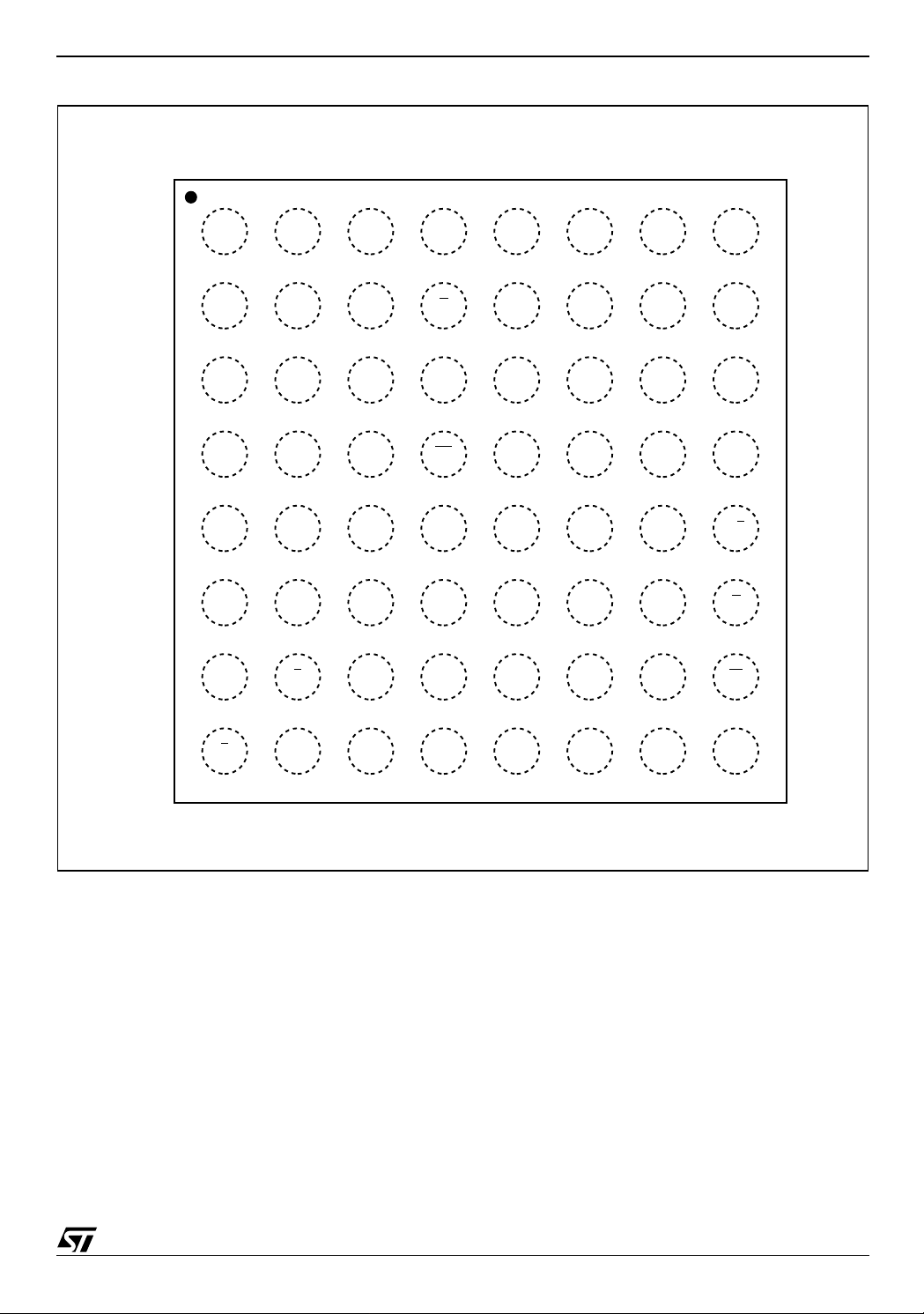
Figure 4. TBGA64 Connections for M58LW128A (Top view through package)
87654321
A
B RA19A2
C
D A16
E
F
G
A1
V
A4 A5
K
A23
DQ0
A6 V
SS
A7A3
A8
A10 A12
A11
DQ10
DQ2B
PP
EA9
RP
DDQ
A13
A14
A15
NC NC
DQ5V
V
DD
NC
NC
NC
NC NC
DQ6
DQ15 RBDQ9DQ8 DQ1 DQ4DQ3
DQ14
A20
A22A18
A21
A17
GDQ12DQ11
W
H
L
NC
V
DD
V
SS
DQ13
V
SSQ
DQ7
NC
AI04316
9/65
M58LW128A, M58LW128B
Figure 5. TBGA80 Connections for M58LW128B (Top view through package)
87654321
A
B RA19A2
C
D NC
E
F
G
A1
A4 A5
DQ24
A8 A22A18
A7
A6A3
DQ25
DQ18
V
SS
A10
A11
DQ27
LDQ17 DQ26 DQ30DQ5DQ3
E
A12A9
V
PP
RP
A13
A14
A15
A23
DQ6WORD
V
DD
A16
A17
NC
DQ28
DQ20 DQ29
W DQ21
A20
DQ22 DQ31DQ19DQ16
A21
NC
DQ23DQ13DQ10
10/65
H
J
K
K DQ15DQ2 DQ12B DQ11 GRB
DQ0
DQ8
DQ1
DQ9 DQ14
V
DD
V
DD
SS
V
SS
DQ4V
V
DDQ
V
V
SSQ
DDQ
V
V
SSQ
DDQ
DQ7
AI04318
Figure 6. Block Addresses
M58LW128A, M58LW128B
M58LW128A, M58LW128B
Word (x16) Bus Width
Address lines A1-A23
7FFFFFh
7F0000h
7EFFFFh
7E0000h
01FFFFh
010000h
00FFFFh
000000h
Note: A l so see Appe ndi x A, Table 28 for a full listing of the Block Addresses
1 Mbit or
64 KWords
1 Mbit or
64 KWords
Total of 128
1 Mbit Blocks
1 Mbit or
64 KWords
1 Mbit or
64 KWords
SIGNAL DESCRIPTIONS
See Figure 2, Logic Diagram and Table 1, Signal
Names, for a brief overview of the signals connected to this device.
Address Inputs (A1-A23). The Address Inputs are used to select the cells to access in the memory array during Bus Read operations either to read or to program data to. During Bus Write operations they control the commands sent to the Command Interface of the internal state m ac hine. Chip Enable must be low when selecting the addresses.
The address inputs are latched on the rising edge
of Chip Enable, Write Enable or Latch Enable,
whichever occurs first in a write operation. The address latch is transparent when Latch Enable is
low, V
. The address is internally latched in a pro-
IL
gram or erase operation.
With a x32 Bus Width, WORD
= VIH, Address Input
A1 is ignored; the Least Significant Word is output
on DQ0-DQ15 and the Most Significant Word is
output on DQ16-DQ31. With a x16 Bus Width,
WORD
on DQ0-DQ15 when A1 is lo w, V
= VIL, the Least Significant Word is ou tput
and the Most
IL,
Significant Word is output on DQ0-DQ15 when A1
is high, V
.
IH
Data Inputs/Outputs (DQ0-DQ31). The Data Inputs/Outputs output the data stored at the selected address during a Bus Read operation, or are used
to input the data during a Program operation. During Bus Write operations they repres ent the commands sent to the Command Interface of the
internal state machine. When used to input data or
write commands they are latched on the rising
edge of Write Enable or Chip Enable, whichever
occurs first.
When Chip Enable and Output Enable are both
low, V
ory array, the Electronic Signature, the Block Protection status, the CFI Information or the contents
of the Status Register. The data bus is high impedance when the chip is deselected, Output E nable
is High, V
Low, V
active the Ready/Busy status is given on DQ7
while DQ0-DQ6 and DQ8-DQ 31 are high impedance.
With a x16 Bus Width, WORD
are not used and are high impedance.
Chip Enable (E
vates the memory control logic, input buffers, decoders and sense amplifiers. Chip Enable, E
V
consumption to the Standby level, I
Output Enable (G
the outputs through the data output buffers during
a read operation. When Output Enable, G
M58LW128B
Double-Word (x32) Bus Width
Address lines A2-A23
(A1 is Don't Care)
3FFFFFh
3F8000h
3F7FFFh
3F0000h
00FFFFh
008000h
007FFFh
000000h
, the data bus outputs data from the mem-
IL
IH,
. When the Program/Erase Controller is
IL
1 Mbit or
32 KDouble-Words
1 Mbit or
32 KDouble-Words
1 Mbit or
32 KDouble-Words
1 Mbit or
32 KDouble-Words
AI06130
or the Reset/Power-Down signal is
= VIL, DQ16-DQ31
). The Chip Enable, E, input acti-
deselects the memory and reduces the power
IH
DD1
.
). The Output Enable, G, gates
, is at V
, at
IH
11/65

M58LW128A, M58LW128B
the outputs are high impedance. Output Enable,
G
, can be used to inhibit the data ou tput during a
burst read operation.
Write Enable (W
). The Write Enable input, W,
controls writing to the Command Interface, Input
Address and Data latches. Both addresses and
data can be latched on the rising edge of Write Enable (also see Latch Enable, L
Reset/Power-Down (RP
).
). The Reset/PowerDown pin can be used to apply a Hardware Reset
to the memory or to temporarily unprotect all
blocks that have been prot e cte d .
A Hardware Reset is achieved by holding Reset/
Power-Down Low, V
, for at least t
IL
Reset/Power-Down is Low, V
, the Status Regis-
IL
PLPH
. When
ter information is cleared and the current is reduced to I
(refer to Table 16, DC
DD2
Characteristics). The device is deselected and
outputs are high impedance. If Reset/PowerDown goes low, V
,during a Block Erase, a Write
IL
to Buffer and Program or a Block Protect/Unprotect the operation is aborted and the data may be
corrupted. In this case the Ready/Bu sy pin stays
low, V
After Reset/Power-Down goes High, V
, for a maximum timing of t
IL
PLPH
+ t
PHRH
, the
IH
.
memory will be ready for Bus Read and Bus Write
operations after t
. Note that Ready/Busy does
RHEL
not fall during a reset, see Ready/Busy Output
section.
During power-up Reset/Power-Down must be held
Low, V
Furthermore it must stay low for t
IL.
VDHPH
after the Supply Voltage inputs become stable.
The device will then be configured in Asynchronous Random Read mode.
See Table 23 and F igure 21, Reset, Power-Down
and Power-up Characteristics, for more details.
Holding RP
at VHH will temporarily unprotect the
protected blocks in the memory. Program and
Erase operations on all blocks will be possible.
In an application, it is recommended to associate
Reset/Power-Down pin, RP
, with the reset sign al
of the microprocessor. Otherwise, if a reset operation occurs while the memory is performing a program or erase operation, the memory may output
the Status Register information instead of being
initialized to the default Asynchronous Random
Read.
Latch Enable (L
). The Bus Interface can be con-
figured to latch the Address Input s on the rising
edge of Latch Enable, L
. In synchronous bus operations the address is latched on the active edge of
the Clock when Latch Enable is Low, V
. Once
IL
latched, the addresses may change without affecting the address used by the memory. When Latch
Enable is Low, V
, the latch is transparent.
IL
Clo c k (K). The Clock, K, is used to synchronize the memory with the external bus during Synchro-
nous Bus Read operations. The Clock can be configured to have an active rising or falling edge. Bus
signals are latched on the active edge of the Clock
during synchronous bus operations. In Synchronous Burst Read m ode the address is latched on
the first active clock edge when Latch Enable is
low, V
, or on the rising edge of Latch Enable,
IL
whichever occurs first.
During Asynchronous Bus operations the Clock is
not used.
Burst Address Advance (B
Advance, B
, controls the advancing of the address
). The Burst Address
by the internal address counter during synchronous bus operations.
Burst Address Advance, B
, is only sampled on the
active clock edge of the Clock when the X- or Y latency time has expired. If Burst Address Advance is Low, V
vances. If Burst Address Advance is High, V
, the internal address counter ad-
IL
IH
, the
internal address counter does not change; the
same data remains on the Data Inputs/Outputs
and Burst Address Advance is not sampled until
the Y-latency expires.
The Burst Address Advance, B
, may be tied to VIL.
Valid Data Ready (R). The Valid Data Ready output, R, is an open drain output that can be used to identify if the memory is ready to output data or not. The Valid Data Ready output is only active during Synchronous Burst Read operat ions when the Burst Length is set to Continuous. The Valid Data Ready output can be configured to be active on the clock edge of the invalid data read cycle or one cycle before. Valid Data Ready Low, VOL, indicates that the data is not, or will not be valid. Valid Data Ready in a high-impedance state indicates that valid data is or will be available.
Unless the Burst Length is set to Cont inuous and
Synchronous Burst Read has been selected, Valid
Data Ready is high-impedance. It may be tied t o
other components with the same Valid Data
Ready signal to create a unique System Ready
signal.
When the system clock frequency is between
33MHz and 50MHz and the Y latency is set to 2,
values of B
sampled on odd clock cycles, starting
from the first read are not considered.
Designers should use an external pull-up resistor
of the correct value to meet the external timing requirements for Valid Data Ready rising. Refer to
Figure 20.
Word Organization (WORD
zatio n inpu t, WORD
, selects the x16 or x32 B us
). The Word Organi-
Width on the M58L W128B. The Word Organization input is not available on the M58LW128A.
When WORD
is Low, VIL, Word-wide x16 Bus
Width is selected; data is read and written to DQ0DQ15; DQ16-DQ31 are at high impedance and A1
12/65

M58LW128A, M58LW128B
is the LSB of the address bus. When WORD is
High, V
, the Double-Word wide x32 Bus Width is
IH
selected and the data is read and written to on
DQ0-DQ31; A2 is the LSB of the address bus and
A1 is don’t care.
Ready/Busy (RB
). The Ready/Busy output, RB,
is an open-drain output that can be used to identify
if the Program/Erase Controller is currently active.
When Ready/Busy is high impedance, the mem ory is ready for any read, program or erase operation. Ready/Busy is Low, V
, during program and
OL
erase operations. When the de vice is busy it will
not accept any additional Program or Erase commands except Program/Erase Suspend. When the
Program/Erase Controller is idle, or suspended,
Ready Busy can float High through a pull-up resistor.
The use of an open-drain output allows the Ready/
Busy pins from several memories to be connected
to a single pull-up resistor. A Low will then indicate
that one, or more, of the memories is busy.
Ready/Busy is not Low during a reset unless the
reset was applied when the Program/Erase Controller was active; Ready/Busy can rise before Reset/Power-Down rises.
Program/Erase Enable (V
Erase Enable input, V
). The Program/
PP
is used to protect all
PP,
blocks, preventing Program and Erase operations
from affecting their data.
When Program/Erase Enable is Low, V
, any pro-
IL
gram or erase operation sent to the Command Interface will cause the V
Status bit (bit3) in the
PP
Status Register to be set. When Program/Erase
Enable is High, V
, program and erase operations
IH
can be performed on unprotected blocks. Program/Erase Enable must be kept High during all
Program, Erase, Block P rotect and Block Unpro-
tect operations, otherwise the operation is not
guaranteed to succeed and data may become corrupt.
V
Supply Voltage. The Supply Voltage, VDD,
DD
is the core power supply. Al l internal c ircuits draw
their current from the V
pin, including the Pro-
DD
gram/Erase Controller.
A 0.1µF capacitor should be connec ted between
the Supply Voltage, V
, and the Ground, VSS, to
DD
decouple the current surges from the power supply. The PCB track widths must be sufficient to
carry the currents required during all operations of
the parts, see Table 16, DC Characteristics, for
maximum current supply requirements.
Input/Output Supply Voltage (V
put/Output Supply Voltage, V
DDQ
). The In-
DDQ
, is the input/output buffer power supply. All input and output pins
and voltage references are powered and measured relative to the Input /Output Suppl y Voltage
pin, V
The Input/Output Supply Volt age, V
ways be equal or less than the V
DDQ
.
, mus t al-
DDQ
Supply Volt-
DD
age, including during Power-Up.
A 0.1µF capacitor should be connec ted between
the Input/Output Supply Voltage, V
Ground, V
from the power supply. If V
, to decouple the current surges
SSQ
and VDD are con-
DDQ
DDQ
, and the
nected together then onl y one decoupling capac itor is required.
Ground (V
). Ground, V
SS
is the reference for
SS,
all core power supply voltages.
Ground (V
). Ground, V
SSQ
is the reference
SSQ,
for input/output voltage measurements. It is essential to connect V
ground
.
SS
and V
to the same
SSQ
13/65

M58LW128A, M58LW128B
BUS OPERATIONS
The bus operations that control the memory are
described in this section, see Tables 2 and 3, Bus
Operations, for a summary. The bus operation is
selected through the Burst Configuration Register;
the bits in this register are described at the end of
this secti on.
On Power-up or after a Hardware Reset the memory defaults to Asynchronous Bus Read and Asynchronous Bus Write, n o other bus operation can
be performed until the Burst Control Register has
been configured.
Synchronous Read operations and Latch Controlled Bus Read operations can only be used to
read the memory array. The Electr onic Sign ature,
CFI or Stat us Register will b e read in asynchro nous mode regardless of the Burst Control Register se tt i n gs.
Typically glitches of less than 5ns on Chip Enable
or Write Enable are ignored by the memory and do
not affect bus operations.
Asynchronous Bus Operation s
For asynchronous bus operations refer to Tabl e 3
together with the text below.
Asynchronous Bus Read. Asynchronous Bus
Read operations read from the memory cells, or
specific registers (Electronic Signature, Status
Register, CFI and Block Prot ection Status) in the
Command Interface. A valid bus operation involves setting the desired address on the Address
Inputs, applying a Low sig nal, V
and Output Enable and keeping Write Enable
High, V
. The Data Inputs/Outputs will output the
IH
value, see Figure 12, Asynchronous Bus Read AC
Waveforms, and Table 17, Asynchronous Bus
Read AC Characteristics, for details of when the
output becomes valid.
Asynchronous Latch Controlled Bus Read.
Asynchronous Latch Controlled Bus Read operations read from the m emory cells. T he address is
latched in the memory before the value is ou tput
on the data bu s, allowing the address to cha nge
during the cycle without affecting the address that
the memo r y uses.
A valid bus operation i nvolves set ting the des ired
address on the Address Inputs, setting Chip Enable and Address Latch Low, V
Write Ena ble Hig h, V
; the address is latched on
IH
the rising edge of Address Latch. Once latched,
the Address Inputs can change. Set Output Enable Low, V
, to read the data on the Data Inputs/
IL
Outputs; see Figure 13, Asynchronous Latch Controlled Bus Read AC Waveforms and Table 18,
Asynchronous Latch Controlled Bus Read AC
Characteristics for details on when the out put becomes valid.
, to Chip Enable
IL
and keeping
IL
Note that, since the Latch Enable input is transparent when set Low, V
, Asynchronous Bus Read
IL
operations can be performed when the memory is
configured for Asynchronous Latch Enable bus
operations by holding Latch Enable Low, V
throughout the bus operation.
Asynchronous Page Read. Asynchronous Page
Read operations are used to read from several addresses within the same memory page. Each
memory page is 8 Words or 4 Double-Words and
has the same A 4-A23, only A1, A2 and A3 may
change.
Valid bus operations are the same as Asynchronous Bus Read operations but with different timings. The first read operation within the page has
identical timings, subsequent reads within the
same page have much sh orter access t i mes. If the
page changes then the normal, longer timings apply again. See Figure 14, Asynchronous Page
Read AC Waveforms and Table 19, Asynchronous Page Read AC Characteristics for details on
when the outputs become valid.
Asynchronous Bus Write. Asynchronous Bus
Write operations write to the Command Interface
in order to send commands to the memory or to
latch addresses and in put data to program. Bus
Write operations are asynchronous, the clock, K,
is don’t care during Bus Write operations.
A valid Asynchronous Bus Write operation begins
by setting the desired address on the A ddress I nputs and setting Latch Enabl e Low, V
. The Ad-
IL
dress Inputs are latched by the Command
Interface on the rising edge of Chip Enable or
Write Enable, whichever occurs first. The Data Inputs/Outputs are la tched by the Comm and Interface on the rising edge of Chip Enable or Write
Enable, whichever occurs first. Output Enable
must remain High, V
, during the whole Asyn-
IH
chronous Bus Write operation. See Figures 15,
and 17, Asynchronous Write AC Wavef orms, and
Tables 20 and 21, Asynchronous Write and Latch
Controlled Write AC Characteristics, for details of
the timing requirements.
Asynchronous Latch Controlled Bus Write.
Asynchronous Latch Controlled Bus W rite operations write to the Command Interface in order to
send commands to the memory or to latch addresses and input data t o p rogram . Bus W r ite operations are asynchronous, the clock , K, is don’t
care during Bus Write operations.
A valid Asynchronous Latch Controlled Bus Write
operation begins by setting the desired address on
the Address Inputs and pulsing Latch Enable Low,
V
. The Address Inputs are latched b y the Com-
IL
mand Interface on the rising edge of Latch Enable,
Chip Enable or Write Enable, whichever occurs
IL
14/65
M58LW128A, M58LW128B
first. The Data Inputs/Outputs are latched by the
Command Interface on the rising edge of Chip Enable or Write Enable, whichever occurs first. Ou tput Enable must remain High, V
, during the
IH
whole Asynchronous Bus Write operation. See
Figures 16 and 18 Asynchronous Latch Controlled
Write AC Waveforms, and Tables 20 and 21,
Asynchronous Write and Latch Controlled Write
AC Characteristics, for details of the timing requirements.
Output Disa bl e . The Data Inputs/Outputs are in the high impedance state when the Output Enable is High.
Standby. When Chip Enable is High, V
IH
, the
puts/Outputs pins are placed in the high impedance state regardless of Output Enable or Write
Enable. The Supply Current is reduced to the
Standby Supply Current, I
During Program or Erase operations the memory
will continue to use the Program/Erase Supply
Current, I
til the operation completes.
Power-Down. The memory is in Power-Down mode when Reset/Power-Down, RP current is reduced to I high impedance, independent of Chip Enable, Output Enable or Write Enable.
memory enters Standby mode and the Data In-
Table 2. Asynchronous Bus Operations
Bus Operation Step E G W RP
Asynchronous Bus Read
Asynchronous Latch
Controlled Bus Read
Asynchronous Page Read
Asynchronous Bus Write
Asynchronous Latch
Controlled Bus Write
Output Disable
Standby
Power-Down X X X
Note: 1. X = Don’t Car e VIL or VIH. High = VIH or VHH.
2. M15 = 1, Bit s M15 and M3 are in the Burst Configura tion Register.
Address Latch
Read
Address Latch
V
ILVILVIH
V
ILVILVIH
V
ILVILVIH
V
ILVILVIH
V
ILVIHVIL
V
ILVIHVIL
V
ILVIHVIH
V
X X High X X X High Z
IH
.
DD1
, for Program or Erase operations un-
DD3
, is Low. The
, and the outputs are
DD2
(2)
M3
High 0 X Address Data Output
High 1
High 1
High 0 X Address Data Output
High X
High X
High X X X High Z
V
IL
L A1-A23 DQ0-DQ31
V
Address High Z
IL
V
IH
V
IL
V
IL
X X X High Z
X Data Output
Address Data Input
Address Data Input
15/65

M58LW128A, M58LW128B
Synchronous Bus Operations
For synchronous bus operat ions refer to Table 3
together with the text below.
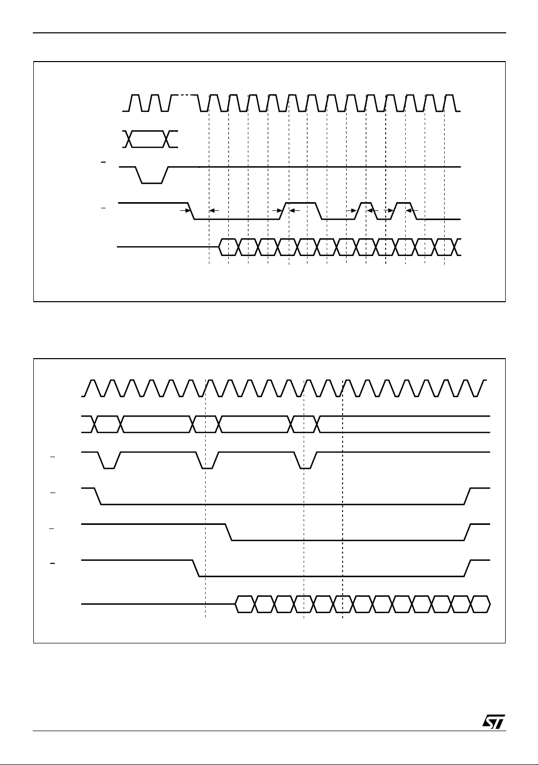
Synchronous Burst Read. Synchronous Burst
Read operations are used to read from the memory at specific times synchronized to an external reference clock. The burst type, length and latency
can be configured. The different configurations for
Synchronous Burst Read operations are described in the Burst Configuration Register section.
A valid Synchronous Burst Read operation begins
when the address is set on the Address Inputs,
Write Enable is High, V
Latch Enable are Low, V
, and Chip Enable and
IH
, during the active edge
IL
of the Clock. The address is latched on the first active clock edge when Latch Enable i s low, or on
the rising edge of Latch Enable, whichever occurs
first. The data becomes available for output after
the X-latency specified in the Burst Control Register has expired. The output buffers are activated
by setting Output E nable Low, V
. See Figure 7
IL
for an example of a Synchron ous Burst Read operation.
The Burst Address Advance input and the Y-latency specified in the Burst Control Register determine whether the internal address counter is
advanced on the active edge of the Clock. When
the internal address counter is advanced the Data
Inputs/Outputs change to output the v alue for t he
next address.
In Continuous Burst mode (Burst Length Bit M2-
M0 is set to ‘111’), one Burst Read operation can
access the entire m emory sequentially and wrap
at the last address. The Burst Address Advance,
B
, must be kept low , VIL, for the appropriate number of clock cycles. If Burst Address Advance, B
is pulled High, V
, the Burst Read will be sus-
IH
pended.
In Continuous Burst Mode , if the starting addres s
is not associated with a page (4 Word or 2 Double
Word) boundary the Va lid Data Ready, R, ou tput
goes Low, V
, to indicate that the data will not be
IL
ready in time and additional wait-states are required. The Valid Data Ready output timing (bit
M8) can be changed in the Burst Configuration
Register.
When using the x32 Bus Width certain X-latencies
are not valid and must not be used; s ee Table 5,
Burst Configuration Register.
The Synchronous Burst Read timing diagrams
and AC Characteristics a re described in the AC
and DC Parameters section. See Figures 19, 20
and Table 22.
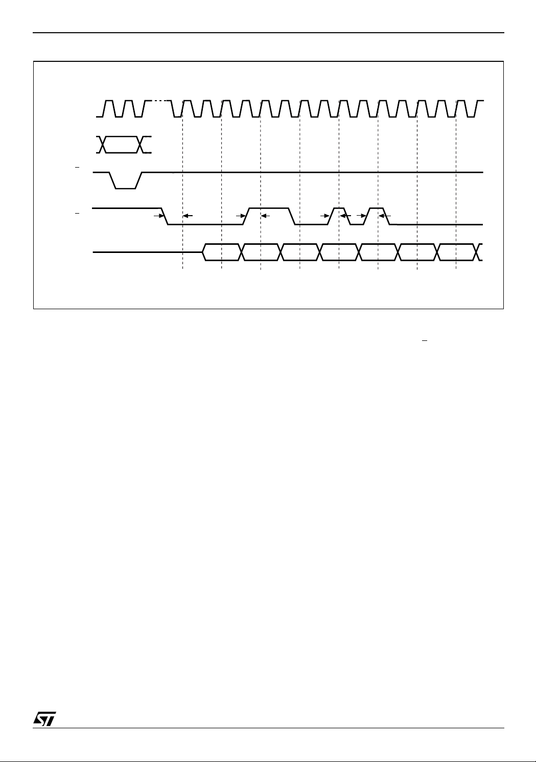
Synchronous Pipelined Burst Read. Synchronous Burst Read operations can be overlapped to
avoid or reduce the X-latency. Pipelined operations should only be used with Burst Configuration
Register bit M9 = 0 (Y-latency setting).
A valid Synchronous Pipelined Burst Read operation occurs during a Sy nchronous Burs t Read operation when the new address is set on the
Address Inputs and a Low pulse is applied to Latch
Enable. The data for the new address becomes
valid after the X-latency specified in the Burst Configuration Register has expired.
For optimum operation the address should be
latched on the correct clock cycle. Table 4 gives
the clock cycle for each valid X- and Y-latency setting. Only these settings are valid, other settings
must not be used. There is always one Y-Latency
period where the data is not valid. If the address is
latched later than the clock cycle s pecified in Tables 4 then additional cycles where the data is not
valid are inserted. See Figure 8 for an example of
a Synchronous Pipelined Burst Read operation.
Here the X-latency is 8, the Y-latency is 1 and the
burst length is 4; the first address is latched on cycle 1 while the next address is latched on cycle 6,
as shown in Table 4.
Synchronous Pipelined Burst Read operations
should only be performed on Burst Lengths of 4 or
8 with a x16 Bus Width or a Burst Length of 4 with
a x32 Bus Width.
Suspending a Pipelined S ynch ronous B urst Read
operation is not recommended.
,
Synchronous Burst Read Suspend. During a
Synchronous Burst Read operation it is possible to
suspend the operation, freeing the data bus for
other higher priority devices.
A valid Synchronous Burst Read operation is suspended when b oth Output Enable an d Burst Address Advance are H igh, V
Advance going High, V
and the Output Enable going High, V
. The Burst Address
IH
, stops the burst counter
IH
IH
data outputs. The Synchronous Burst Read operation can be resumed by setting Output Enable
Low. See Figure 7 for an example o f a Synchronous Burst Read Suspend operation.
, inhibits the
16/65
M58LW128A, M58LW128B
Table 3. Synchronous Burst Read Bus Operation s
Bus Operation Step E G RP
X
VILV
VILV
VILV
VILV
X
V
V
Address Latch
Read (no address advance)
Read (with address advance)
Synchronous Burst Read
Pipelined Synchronous
Burst Read
Read Suspend
Read Resume (no address
advance)
Read Resume (with address
advance)
Read Abort
Note: 1. X = Don’t Care, VIL or VIH.
2. M15 = 0, Bit M 15 i s in the Burs t C onfiguration Register.
3. T = tra nsition, see M6 in the Burst Conf i guration Register for details on the active edge of K.
V
IL
V
IL
V
IL
V
ILVIHVIH
V
IL
V
IL
V
IH
Table 4. Addre s s Lat ch Cycle for Optimum Pipelin ed S ynchronous Burst Read
X-Latency Y-Latency
Burst Length = 4 Burst Length = 8
81 6 10
Address Latch Clock Cycle
K
IH
IH
IH
IH
IH
IH
(3)
L B
V
T
IL
TX
TX
XX
TX
TX
XX
A1-A23
DQ0-DQ31
X Address Input
V
Data Output
IH
V
Data Output
IL
V
IH
V
IH
V
IL
X
High Z
Data Output
Data Output
High Z
91 7 11
12 1 10 14
13 1 11 15
15 2 11 19
17/65
M58LW128A, M58LW128B
Figure 7. Synchronous B urst Re ad Operation
1
0
K
Address
Inputs
L
B
Data Inputs/
Outputs
Note: I n this exa mple t he Bur st Co nfigur ati on Reg ist er is set with M 2-M 0 = 001 (B urst Lengt h = 4 Wo rds or Doubl e Word s) , M6 = 1 (Valid
Clock Edge = Rising Clock Edge), M7 = 0 or 1 (Burst Type = Interleaved or Sequential), M9 = 0 (Y-Latency = 1), M14-M11 = 0011 (X-
Latency = 8) and M15 = 0 (Rea d Se l ect = Synchronous Burst Read), other bi ts are don’t care.
Q1
X-1
X
tBLKH
Q1
X+1
Q2
tBHKH
tBHKH
Q5Q5Q5Q4Q3 Q7Q6 Q8Q8Q7
tBHKH
AI03454b
Figure 8. Exam pl e Synchronous Pipelined Burst Read Op era ti on
01234567891011121314
K
15
Address
Inputs
L
E
G
B
Data
Inputs/ Outputs
Note: I n this exa mple t he Bur st Co nfigur ati on Reg ist er is set with M 2-M 0 = 001 (B urst Lengt h = 4 Wo rds or Doubl e Word s) , M6 = 1 (Valid
Clock Edge = Rising Clock Edge), M7 = 0 or 1 (Burst Type = Interleaved or Sequential), M9 = 0 (Y-Latency = 1), M14-M11 = 0011 (XLatency = 8) and M15 = 0 (Rea d Se l ect = Synchronous Burst Read), other bi ts are don’t care.
Q1 R1 S1
Q1
Q2 Q3 Q4 NV R1 R2 R3 R4 NV S1 S2
NV= Not Valid
S3
AI03455
18/65
M58LW128A, M58LW128B
Figure 9. Example Burst Address Advance and Burst Abort operations
1
0
K
Address
Inputs
L
B
Data Inputs/
Outputs
Note: 1. In this exam pl e the Bur st Co nf igurat ion Reg ister is set with M 2-M 0 = 010 (B urst Lengt h = 8 Words ), M 6 = 1 (V alid C loc k Edg e =
Rising Clock Edge), M 7 = 0 or 1 (Burst Type = In te rl eaved or Se quential) , M9 = 1 (Y-Lat ency = 2), M14-M11 = 0011 (X-Latency =
8) and M15 = 0 (Read Select = Sy nchronous Burst Read ), other bits a re don’t care.
2. Whe n t he system clock fre quency is be tween 33MHz and 50MHz and th e Y latenc y i s set to 2, values of B
cycles, starting from t he first read are not conside red.
Q1
X-2
tBLKH
X
Q1 Q2
X+2
tBHKH
X+6X+4 X+12X+10X+8
tBHKH
Q3 Q4 Q4
tBHKH
Q4Q3
AI03457b
sampled on odd clock
19/65

M58LW128A, M58LW128B
Burst Configuration Register
The Burst Configuration Register is used to configure the type of bus access that the memory will
perform.
The Burst Configuration Register is set through
the Command Interface and will retain its information until it is re-configured, the device is reset, or
the device goes into Reset/Power-Down mode.
The Burst Configuration Register bits are described in Table 5. They specify the selection of
the burst length, burst type, burst X and Y latencies and the Read operation.
Read Select Bit (M15). The Read Select bit,
M15, is used to switch between asynchronous and
synchronous Bus Read operations. When the
Read Select bit is set to ’1’, Bus Read operations
are asynchronous; when the Read Select but is
set to ’0’, Bus Read operations are synchronous.
On reset or power-up the Read Sel ect bi t is set
to’1’ for asynchronous accesses.
X-Latency Bits (M14-M11). The X-Latency bits are used during Synchronous Bus Read operations to set the number of clock cycles between the address being latched and the first data becoming available. For correct operation the X-Latency bits can only assume the values in Table 5, Burst Configuration Register. The X -Latency bits should also be sele cted in con junction with Table 8, Burst Performance to ensure valid settings.
Y-Latency Bit (M9). The Y-Latency bit is used
during Synchronous Bus Read operations to set
the number of clock cycles between consecutive
reads. The Y-Latency value depends on both the
X-Latency value and the setting in M9.
When the Y-Latency is 1 the data changes each
clock cycle; when the Y-Latency is 2 the data
changes every seco nd clock cycle. See Tab le 5,
Burst Configuration Register and Table 8, Burst
Performance, for valid co mbinations of the Y-Latency, the X-Latency and the Clock frequency.
Valid Data Ready Bit (M8). The Valid Data Ready bit controls the timing of the Valid Data
Ready output pin, R. When the Valid Data Ready
bit is ’0’ the Valid Data Ready output pin is driven
Low for the active clock edge when invalid data is
output on the bus. When the Valid Data Ready bit
is ’1’ the Valid Data Ready output pin is driven Low
one clock cycle prior to invalid data being output
on the bus.
Burst Type Bit ( M7 ). The Burst Type bit is used to configure the sequence of addresses read as sequential or interleaved. When the Burst Type bit is ’0’ the memory outputs from interleaved addresses; when the Burst Type bit is ’1’ the memory outputs from sequential ad dresses. See Tables 6 and 7, Burst Type Definition, for t he sequence of addresses output from a give n starting a ddress in each mode.
Valid Clock Edge Bit (M6). The Valid Clock Edge bit, M6, is used to configure the active edge of the Clock, K, during Synchronous Burst Read operations. When the Valid Clock Edge bit is ’0’ the falling edge of the Clock is the active edge; when the Valid Clock Edge bit is ’1 ’ the rising edge of the Clock is active.
Latch Enable Bit (M3). The Latch Enable bit is
used to select between Asynchronous Random
Read and Asynchronous La tch Enable Controlled
Read. When the Latch Enable bit is set to ‘0’ Random read is selected; when it is set to ‘1’ Latch Enable Controlled Read is selected. To enable these
Asynchronous Read configuration s M15 must be
set to ‘1’.
Burst Length Bit (M2-M0). The Burst Length bits set the maximum number of Words or DoubleWords that can be ou tput during a Synchronous Burst Read operation before the address wraps.
Table 5, Burst Configuration Register gives the
valid combinations of the Burst Length bits that the
memory accepts; Tables 6 and 7, Burst Type Definition, give the sequence of addresses output
from a given starting address for each length.
M10, M5 an d M4 are reserved for future use.
20/65

Table 5. Burst Configuration Registe r
Address
Bit
17 M15
Mnemonic Bit Name
Read
Select
Reset
Value
1
M58LW128A, M58LW128B
Value Description
0 Synchronous Burst Read x16 or x32
1 Asynchronous Bus Read x16 or x32
Valid Bus
Width
16
to
13
11 M9
10 M8
M14-M11 X-Latency XXXX
Y-Latency
Valid Data
Ready
0010
0011 X- Laten cy = 8 x16 or x32
0100 X- Laten cy = 9 x16 or x32
0101
0110
1001 X-Latency = 12 x16 only
1010 X-Latency = 13 x16 only
1011
1101 X- Laten cy = 15 x16 or x32
Others Reserved, Do Not Use.
X
X
X-Latency = 7, use only with Continuous Burst
Length
X-Latency = 10, use only with Continuous Burst
Length
X-Latency = 11, use only with Continuous Burst
Length
X-Latency = 13, use only with Continuous Burst
Length
When X-Latency < 13, Y-Latency = 1
0
When M14-M11 = 1011 or 1101, Y-Latency = 2
When X-Latency ≤15 but M14-M11≠1011 or
1101, Y-Latency = 2,
1
When M14-M11=1011 or 1101 DO NOT USE.
0 R valid Low during valid Clock edge x16 or x32
1 R valid Low one cycle before valid Clock edge x16 or x32
x16 or x32
x16 only
x16 only
x16 or x32
x16 or x32
x16 or x32
9 M7 Burst Type X
8M6
5M3
4
to
2
M2-M0
Valid Clock
Edge
Latch
Enable
Burst
Length
XXX
0 Interleaved x16 or x32
1 Sequential x16 or x32
0 Falling Clock edge x16 or x32
X
1 Rising Clock edge x16 or x32
0 Random Read x16 or x32
0
1 Latch Enable Controlled Read x16 or x32
100 1 Word or Double-Word x16 or x32
101 2 Words or Double-Words x16 or x32
001 4 Words or Double-Words x16 or x32
010 8 Words x16 only
111 Continuou s x16 or x32
Others Reserved, Do Not Use.
21/65

M58LW128A, M58LW128B
Table 6. Burst Type Definition (x16 Bus Width)
Starting Addres s
Burst Length
2
4
8
(binary)
A3 A2 A1
XX0 0, 1 0, 1
XX1 1, 0 1, 0
X00 0, 1, 2, 3 0, 1, 2, 3
X01 1, 2, 3, 0 1, 0, 3, 2
X10 2, 3, 0, 1 2, 3, 0, 1
X11 3, 0, 1, 2 3, 2, 1, 0
000 0, 1, 2, 3, 4, 5, 6, 7 0, 1, 2, 3, 4, 5, 6, 7
001 1, 2, 3, 4, 5, 6, 7, 0 1, 0, 3, 2, 5, 4, 7, 6
010 2, 3, 4, 5, 6, 7, 0, 1 2, 3, 0, 1, 6, 7, 4, 5
011 3, 4, 5, 6, 7, 0, 1, 2 3, 2, 1, 0, 7, 6, 5, 4
100 4, 5, 6, 7, 0, 1, 2, 3 4, 5, 6, 7, 0, 1, 2, 3
101 5, 6, 7, 0, 1, 2, 3, 4 5, 4, 7, 6, 1, 0, 3, 2
110 6, 7, 0, 1, 2, 3, 4, 5 6, 7, 4, 5, 2, 3, 0, 1
111 7, 0, 1, 2, 3, 4, 5, 6 7, 6, 5, 4, 3, 2, 1, 0
Sequential
(decimal)
Interleaved
(decimal)
Continuous A A, A+1, A+2... Not Valid
Note: X = 0 or 1.
Table 7. Burst Type Definition (x32 Bus Width)
Starting Addres s
Burst Length
2
4
8 Not Valid
Continuous A A, A+1, A+2... Not Valid
Note: X = 0 or 1.
(binary)
A3 A2
X0 0, 1 0, 1
X1 1, 0 1, 0
00 0, 1, 2, 3 0, 1, 2, 3
01 1, 2, 3, 0 1, 0, 3, 2
10 2, 3, 0, 1 2, 3, 0, 1
11 3, 0, 1, 2 3, 2, 1, 0
Sequential
(decimal)
Interleaved
(decimal)
22/65

M58LW128A, M58LW128B
Table 8. Burst Performance
X-Latency Y-Latency Bus Width Clock Frequency Mode
7
continuous only
8
9
7
8
9
10
11
12
13
10
11
12
13
13
15 continuous, length
1
x16, x32
2
1
x16 only
2
2(M9=0) x16, x32
33 MHz
≤
50 MHz
≤
66 MHz
≤
continuous, length
continuous only
continuous, length
continuous only
continuous, length
continuous only
continuous, length
continuous only
23/65

M58LW128A, M58LW128B
COMMAND INTERFACE
All Bus Write operations t o the me mory are in terpreted by the Command Interface. Commands
consist of one or more sequential Bus Write operations. The Commands are summarized in Table
9, Commands. Refer to Table 9 in conjunction with
the text descriptions below.
After Power-Up or a Reset operation the memory
enters Read mode.
Synchronous Read operations and Latch Controlled Bus Read operations can only be used to
read the memory array. The Electr onic Sign ature,
CFI or Status Register will be read in Asynchronous mode regardless of the Burst Control Register settings. Once the memory returns to Read
Memory Array mode the bus will resume the setting in the Burst Configuration Register automatically.
Read Memory A rray Command. The Read Memory Array command returns the memory to Read
mode. One Bus Write cycle is required to issue the
Read Memory Array command and return the
memory to Read mode. Once the command is issued the memory remains in Read mode until another command is issued. From Read mode Bus
Read operations will access the memory array.
While the Program/Erase Controller is executing a
Program, Erase, Bl ock Protect or Blocks Unprotect operation the memory will not accept the Read
Memory Array command until the operation completes.
Read Electronic S ignature C o mmand. The Read
Electronic Signature command is used to read the
Manufacturer Code, the Device Code and the
Block Protection Status. One Bus Write cycle is required to issue the Read Electronic Signature
command. Once the command is issued subsequent Bus Read operations read the Manufacturer
Code, the Device Code or the Block Protection
Status until another command is issued; see Table
10, Read Electronic Signature.
Read Query Command. The Read Query Command is used to read data from the Common Flash Interface (CFI) Memory Area. One Bus Write cycle is required to issue the Read Query Command. Once the command is issued subsequent Bus Read operations read from the Common Flash Interface Memory Area. See Appendix B, Tables 29, 30, 31, 32, 33 and 34 for details on the information contained in the Common Flash Interface (CFI) memory area.
Note that the addresses for the Common Flash Interface Memory Area are A1-A23 for the
M58LW128A and A2-A23 for the M58LW128B, regardless of the Bus Width selected.
Read Statu s Register Command. The Read Status Register command is used to read the Status
Register. One Bus Write cycle is required to issue
the Read Status Register command. Once the
command is issued subsequent Bus Read operations read the Status Register until another command is issued.
The Status Register information is present on the
output data bus (DQ1-DQ 7) when both Chip Enable and Output Enable are low, V
.
IL
See the section on the Status Register and Table
12 for details on the definitions of the Status Register bits
Clear Status Register Command. The Clear Status Register command can be used to reset bits 1,
3, 4 and 5 in the Status Register to ‘0’. One Bus
Write is required to issue the Clear Status Register
command.
The bits in the Status Register are stic ky and do
not automatically return to ‘0’ when a new Write to
Buffer and Program, Erase, Block Protect or Block
Unprotect command is issued. If any error occurs
then it is essential to clear any error bits in the Status Register by issuing the Clear Status Register
command before attempting a new Program,
Erase or Resume command.
Block Erase Command. The Block Erase command can be used to e rase a block. I t sets all of
the bits in the block to ‘1’. All previous data in the
block is lost. If the block is protected then the
Erase operation will abort, the data in the block will
not be changed and the Status Register will output
the error.
Two Bus Write operations are required to issue the
command; the second Bus Write cycle latches the
block address in the internal state machine and
starts the Program/Erase Controller. Once the
command is issued subsequent Bus Read operations read the Status Register. See the section on
the Status Register for details on the definitions of
the Status Register bits.
During the Erase operation the memory will only
accept the Read Status Register command and
the Program/Erase Su spend command. All ot her
commands will be ignored. Typical Erase times
are given in Table 11.
See Appendix C, Figure 27, Block Erase Flowchart and Pseudo Code, for a suggested flowchart
on using the Block Erase command.
Write to Buffer and Program Command. The Write to Buffer and Program comm and is used to program the memory array.
Up to 2 pages of 8 Words (or 4 Double Words) can
be loaded into the Write Buffer and program med
into the memory. The 2 pages are selected by address A4. Each Write Buffer has the same A5 -A23
addresses.
24/65

M58LW128A, M58LW128B
Four successive steps are required to issue the
command.
1. One Bus Write operation is required to set up
the Write to Buffer and Program Comm and. Issue the set up command with the selected
memory Block Address where the program operation should occur (any address in the block
where the values will be programmed can be
used). Any Bus Read operations will start to output the Status Register after the 1st cycle.
2. Us e one Bus Write operation to write the same
block address along with the value N on the
Data Inputs/Output, where N+1 is the number of
Words (x16 Bus Wi dth) or Double Words (x32
Bus Width) to be programmed.
3. Us e N+1 Bus Write operations to load the address and data for each Word or Double Word
into the Write Buffer. See the constraints on the
address combinations listed below. The addresses must have the same A5-A23.
4. Finally, use one Bus Write operation to issue the
final cycle to confirm the command and start the
Program operation.
Invalid address combinations or failing to follow
the correct sequence of Bus Write cycles will set
an error in the Status Register and abort the operation without affecting the data in the memory array. The Status Register should be cleared before
re-issuing the command.
The minimum buffer size f or a program operation
is an 8 Word (or 4 Doub le W ord) page. Inside the
page the 8 Words a re select ed by addres ses A3,
A2 and A1.
For any page, only one Write to Bu ffer and Program Command can be issued inside a previously
erased block. Any further Program operations on
that page must be preceded by an Erase operation
on the respective block.
If the block being program m ed i s prote cted an error will be set in the Status Register and the operation will abort without affecting the data in the
memory array. The block must be unprotected using the Blocks Unprotect command or by using the
Blocks Temporary Unprotect feature of the Reset/
Power-Down pin, RP
.
See Appendix C, Figure 25, Write to Buffer and
Program Flowchart and Pseudo Code, for a suggested flowchart on using the W rite to Buf fer and
Program command.
Program/Erase Suspend Command. The Program/Erase Suspend command is used to pause a
Write to Buffer and Program or Erase operation.
The command will on ly be acc ep t ed du ring a Program or an Erase operation. It can be issued at
any time during an Erase operation but will only be
accepted during a Write to Buffer and Program
command if the Program/Erase Controller is running.
One Bus Write cycle is required to i ssue the P rogram/Erase Suspend command and pause the
Program/Erase Controller. Once the command is
issued it is necessary to poll the Program/Erase
Controller Status bit (bit 7) to find out when the
Program/Erase Controller has paused; no other
commands will be accepted until the Program/
Erase Controller has paused. After the Program/
Erase Controller has paused, the memory will continue to output the Status Register until another
command is issued.
During the polling period between issuing the Program/Erase Suspend command and the Program/
Erase Controller pausing it is possible for the operation to complete. Once the Program/Erase
Controller Status bit (bit 7) i ndicates that the P rogram/Erase Controller is no longer active, the Program Suspend Status bit (bit 2) or the Erase
Suspend Status bit (bit 6) can be used to determine if the operation has completed or is suspended. For timing on the delay between issuing the
Program/Erase Suspend command and the Program/Erase Controller pausing see Table 11.
During Program/Erase Suspend the Read Memory Array, Read Status Register, Read Elect ronic
Signature, Read Query and Program/Erase Resume commands will be accepted by the Command Interface. Additionally, if the suspended
operation was Erase then the W rite to B uffer and
Program, and the Program Suspend commands
will also be ac cepted. W hen a program o peration
is completed inside a Block Erase Suspend the
Read Memory Array command m ust be issued to
reset the device in Read mode, then the Erase Resume command can be issued to complete the
whole sequence. Only the blocks not being erased
may be read or programmed correctly.
See Appendix C, Figure 26 , Program Suspend &
Resume Flowchart and Pseudo Code, and Figure
28, Erase Suspend & Resume Flowchart and
Pseudo Code, for suggested flowcharts on using
the Program/Erase Suspend command .
Program / Erase Resume Command. The Program/Erase Resume com m and c an be used to restart the Program/Erase Controller after a
Program/Erase Suspend operat ion h as paused it.
One Bus Write cycle is required to i ssue the P rogram/Erase Resume command. Once the command is issued subsequ ent Bus Read operations
read the Status Register.
Set Burst Configuration Register Command.
The Set Burst Configuration Register command is
used to write a new value t o the Burst Conf iguration Control Register which defines the burst
length, type, X and Y latencies, Synchronous/
25/65

M58LW128A, M58LW128B
Asynchronous Read mode and the valid Clock
edge configuration.
Two Bus Writ e cycles a re required to i ssue the Set
Burst Configuration Register command. Once the
command is issued the memory returns to Read
mode as if a Read Mem ory Array command had
been issued.
The value for the Burst Configuration Register is
always presented on A2-A17, regardless of the
bus width that is selected. M0 is on A2, M1 on A3,
etc.; the other address bits are ignored.
Block Protect Command. The Block Protect command is used to protec t a block and prevent Program or Erase operations from changing the data in it. Two Bus Write cycles are required to issue the Block Protect command; the second Bus Write cycle latches the block address in the internal state machine and sta rt s the Program/Erase Controller. Once the command is issued subsequent Bus Read operations read the Status Register. See the section on the Status Register for details on the definitions of the Status Register bits.
During the Block Protect operation the memory will
only accept the Read Sta tus Register command.
All other commands will be ignored. Typical Block
Protection times are given in Table 11.
The Block Protection bits are non-volatile, once
set they remain set through Reset and PowerDown/Power-Up. They are cleared by a Blocks
Unprotect command or temporary disabled by
raising the Reset/Power-Down pin to V
HH
and
holding it at that level throughout a Block Erase or
Write to Buffer and Program command.
Blocks Unprotect Command. The Blocks Unprotect command is used to unprotect all of the blocks. Two Bus Write cycles are requir ed to issue the Blocks Unprotect command ; the second Bus Write cycle starts the Program/Erase Controller. Once the command is issued subsequent Bus Read operations read the Status Register. See the section on the Stat us Register for details on the definitions of the Status Register bits.
During the Block Unprotect operation the memory
will only accept the Read Status Register command. All other commands will be ignored. Typical
Block Protection times are given in Table 11.
26/65

M58LW128A, M58LW128B
Table 9. Commands
Bus Write Operations
Command
Cycles
Read Memory Array 1 X FFh
Read Electronic Signature 1 X 90h
Read Query 1 X 98h
Read Status Register 1 X 70h
Clear Status Register 1 X 50h
Block Erase 2 X 20h BA D0h
Write to Buffer and Program 4 + N BA E8h BA N PA PD X D0h
Program/Erase Suspend 1 X B0h
Program/Erase Resume 1 X D0h
Set Burst Configuration Register 2 BCR 60h BCR 03h
Block Protect 2 BA 60h BA 01h
Blocks Unprotect 2 X 60h X D0h
Note: X Don’t C are; PA Program Address; PD P rogram Data; BA A ny address in th e Block; N+1 Num ber of Addresse s to Program;
BCR Burst Confi guration Register value.
1st 2nd Subsequent Final
Addr Data Addr Data Addr Data Addr Data
Table 10. Read Electronic Signature
Code
Bus Width
Manufacturer Code
Device Code
Block Protection Status
Note: 1. SBA is the Start Base Ad dress of each bl ock.
2. DQ3 1-DQ16 are av ai l able in the M58LW128B only.
3. x32 Bus Width is available in th e M 58LW128B only.
4. The address is presented on A22-A2 in x32 mode, and on A2 2-A1 in x16 mode.
(3)
Address
x16
000000h
x32 00000020h
x16
000001h
x32 00008819h (M58LW128B)
x16
(1)
+02h
SBA
x32
(4)
Data (DQ31-DQ0)
(2)
0020h
8818h (M58LW128A)
8819h (M58LW128B)
0000h (Block Unprotected)
0001h (Block Protected)
00000000h (Block Unprotected)
00000001h (Block Protected)
27/65

M58LW128A, M58LW128B
Table 11. Program, Erase Times and Progr am Eras e Endur ance Cycles
M58LW128A/B
Parameters
Min Typ
Typical after
100k W/E Cycles
Max
Block (1Mb) Erase 0.75 0.75 5 s
Block Program 0.8 0.8 s
Program Write Buffer 192 192 µs
Program Suspend Latency Time 3 10 µs
Erase Suspend Latency Time 10 30 µs
Block Protect Time 192 µs
Blocks Unprotect Time 0.75 s
Program/Erase Cycles (per Block) 100,000 cycles
Data Retention 20 years
Note: (TA = 0 to 70°C; VDD = 2.7V to 3.6V; V
DDQ
=1.8V)
Unit
28/65

STATUS REGISTER
The Status Register provides information on the
current or previous Program, Erase, Block Protect
or Blocks Unprotect operation. The various bits in
the Status Register convey information and errors
on the operation. They are output on DQ7-DQ0.
To read the Status Register the Read Status Register command can be issued. The Status Register
is automatically read after Program, Erase, Block
Protect, Blocks Unprotect and Program/Erase Resume commands. The Status Register can be
read from any address.
The Status Register can only be read using Asynchronous Bus Read operations. Once the memory
returns to Read Memory Array mode the bus will
resume the setting in the Burst Configuration Register automatically.
The contents of the Status Register can be updated during an Erase or Program operation by toggling the Output Enable pin or by dis-activating
(Chip Enable, V
able and Output Enable, V
) and then reactivating (Chip En-
IH
) the device.
IL
During a Program, Block Erase, Block Prote ct or
Block Unprotect operation only bit 7 is valid, all
other bits are high impedance. Once the operation
is complete bit 7 is High and all other Status register bits are valid.
Status Register bits 5, 4, 3 and 1 are associated
with various error conditions and can only be reset
with the Clear Status Register command. The Status Register bits are summarized in Table 12, Status Register Bits. Refer to Table 12 in conjunction
with the following text descriptions.
Program/Erase Controller Status (Bit 7). The Progra m/Erase Controller Status bit indicates whether
the Program/Erase Controller is active or inactive.
When the Program/Erase Controller Status bit is
Low, V
, the Program/Erase Controller is active
OL
and all other Status Register bits are High Impedance; when the bit is High, V
, the Program/
OH
Erase Controller is inactive.
The Program/Erase Controller Status is Low im-
mediately after a Program/Erase Suspend command is issued until the Program/Erase Controller
pauses. After the Program/Erase Controller pauses the bit is High.
During Program, Erase, Block Protect and Blocks
Unprotect operations the Program/Erase Controller Status bit can be polled to find the end of the
operation. The other bits in the Status Register
should not be tested until the Program/Erase Controller completes the operation and the bit is High.
After the Program/Erase Cont roller completes its
operation the Erase S tatus, Program Status and
Block Protection Status bits should be tested for
errors.
M58LW128A, M58LW128B
Erase Suspend Status (Bit 6). The Erase Sus-
pend Status bit indicates that an Erase o peration
has been suspended and is waiting to be resumed. The Erase Suspend Status should only be
considered valid when the Program/Erase Controller Status bit is High (Program/Erase Controller
inactive); after a Program/Erase Suspend command is issued the memory may still complete the
operation rather than entering the Suspend mode.
When the Erase Suspend Statu s bit is Low, V
the Program/Erase Controller is active or has completed its operation; when the bit is High, V
Program/Erase Suspend com mand has been issued and the memory is waiting for a Program/
Erase Resume command.
When a Program/Erase Re sume command is issued the Erase Suspend Status bit returns Low.
Erase Status (Bit 5). The Erase Status bit can be
used to identify if the memory has failed to verify
that the block has erased correctly or that all
blocks have been unprotected successfully. The
Erase Status bit should be read once the Program/
Erase Controller Status bit is High (Program/Erase
Controller inactive).
When the Erase St atu s bit i s Low, V
, the mem-
OL
ory has successfully verified that the block has
erased correctly or all blocks have been unprotected successfully. When the Erase Status bit is
High, V
, the erase operation has failed. De-
OH
pending on the cause of the failure othe r Status
Register bits may also be set to High, V
■ If only the Erase Status bit (bit 5) is set High,
then the Program/Erase Controller has
V
OH,
OH
applied the maximum number of pulses to the
block and still failed to verify that the block has
erased correctly or that all the blocks have been
unprotected successfully.
■ If the failure is due to an erase or blocks
unprotect with V
(bit 3) is also set High, V
■ If the failure is due to an erase on a protected
low, VOL, then VPP Status bit
PP
OH
.
block then Block Protection Status bit (bit 1) is
also set High, V
■ If the failure is due to a program or erase
OH
.
incorrect command sequence then Program
Status bit (bit 4) is also set High, V
OH
.
Once set High, the Erase Status bit can only be reset Low by a Clear Status Register command or a
hardware reset. If set High it should be reset before a new Program or Erase command is issued,
otherwise the new command will appear to fail.
Program Status (Bit 4). The Program Status bit
is used to identify a Program or Block Pr otect failure. The Program S tatus bit shoul d be read once
OL
, a
OH
.
,
29/65

M58LW128A, M58LW128B
the Program/Erase Controller Status bit is High
(Program/Erase Controller inactive).
When the Program Status bit is Low, V
OL
, the
memory has successfully verified that the Write
Buffer has programmed correc tl y or the block is
protected. When the Program Status bit is High,
V
, the program or block protect operation has
OH
failed. Depending on the cause of the failure other
Status Register bits may also be set to High, V
■ If only the Program Status bit (bit 4) is set High,
V
then the Program/Erase Controller has
OH,
OH
applied the maximum number of pulses to the
byte and still failed to verify that the Write Buffer
has programmed correctly or that the Block is
protected.
■ If the failure is due to a program or block protect
with V
also set High, V
■ If the failure is due to a program on a protected
low, VOL, then VPP Status bit (bit 3) is
PP
OH
.
block then Block Protection Status bit (bit 1) is
also set High, V
■ If the failure is due to a program or erase
OH
.
incorrect command sequence then Erase
Status bit (bit 5) is also set High, V
OH
.
Once set High, the Program Status bit can only be
reset Low by a Clear Status Register command or
a hardware reset. If set High it should be reset before a new Program or Erase command is issued,
otherwise the new command will appear to fail.
Status (Bit 3). The VPP Status bit can be
V
PP
used to identify if a Program, Erase, Block Protection or Block Unprotection operation has been a ttempted when V
is Low, VIL. The VPP pin is only
PP
sampled at the beginnin g of a Program or Erase
operation.
When the V
Status bit is Low, VOL, no Program,
PP
Erase, Block Protection or Block Unprotection operations have been attempted with V
Low, VIL,
PP
since the last Clear Status Register command, or
hardware reset. When the V
V
, a Program, Erase, Block Protection or B lock
OH
Status bit is High,
PP
Unprotection operation has been a ttempted with
Low, VIL.
V
PP
Once set High, the V
Status bit can only be reset
PP
by a Clear Status Register command or a hardware reset. If set High it should be reset befo re a
new Program, Erase, Block Protection or Block
Unprotection command is issued, otherwise the
new command will appear to fail.
Program Suspend Status (Bit 2). The Program
Suspend Status bit indicates that a Program oper-
.
ation has been suspended and is waiting to be resumed. The Program Suspend Status should only
be considered valid when the Program/Erase
Controller Status bit is High (Program/Erase Controller inactive); after a Program/Erase Suspend
command is issued the memory may still complete
the operation rather than entering the Suspend
mode.
When the Program Suspend Status bit is Low,
, the Program/Erase Controller is active or has
V
OL
completed its operation; when the bit is High, V
a Program/Erase Suspend command has been issued and the memory is waiting for a Program/
Erase Resume command.
When a Program/Erase Re sume command is issued the Program Suspend Status bit returns Low.
Block Protection Status (Bit 1). The Block Protection Status bit can be used to identify if a Program or Erase operation has tried to modify the
contents of a protected block.
When the Block Protection Status bit is Low, V
no Program or Erase operations have been attempted to protected blocks si nce the last Clear
Status Register command or hardware reset;
when the Block Protection Status bit is High, V
a Program (Program Status bit 4 set High) or
Erase (Erase Status bit 5 set High) operation has
been attempted on a protected block.
Once set High, the Block Protection Status bit can
only be reset Low by a Clear Status Register command or a hardware reset. If set High it should be
reset before a new Program or Erase command is
issued, otherwise the new command will appear to
fail.
Reserved (Bit 0). Bit 0 of the Status Register is
reserved. Its value should be masked.
OH
OL
OH
,
,
,
30/65

M58LW128A, M58LW128B
Table 12. Status Register Bits
Operation Bit 7 Bit 6 Bit 5 Bit 4 Bit 3 Bit 2 Bit 1 RB
Program/Erase Controller Active ‘0’ Hi-Z
Write Buffer not ready ‘0’ Hi-Z
Write Buffer ready ‘1’
Program suspended ‘1’
Program/Block Protect completed successfully ‘1’
Program/Block Protect failure due to incorrect command
sequence
Program/Block Protect failure due to V
PP
Error
’1’
’1’
Program failure due to Block Protection ‘1’
Program/Block Protect failure due cell failure or unerased cell ‘1’
(1)
X
X
X
X
X
X
X
‘0’ ‘0’ ‘0’ ‘0’ ‘0’ Hi-Z
(1)
‘0’ ‘0’ ‘0’ ‘1’ ‘0’ Hi-Z
(1)
‘0’ ‘0’ ‘0’ ‘0’ ‘0’ Hi-Z
(1)
‘1’ ‘1’ ‘0’ ‘0’ ‘0’ Hi-Z
(1)
‘0’ ‘1’ ‘1’ ‘0’ ‘0’ Hi-Z
(1)
‘0’ ‘1’ ‘0’ ‘0’ ‘1’ Hi-Z
(1)
‘0’ ‘1’ ‘0’ ‘0’ ‘0’ Hi-Z
Erase suspended ‘1’ ‘1’ ‘0’ ‘0’ ‘0’ ‘0’ ‘0’ Hi-Z
Erase/Blocks Unprotect completed successfully ‘1’ ‘0’ ‘0’ ‘0’ ‘0’ ‘0’ ‘0’ Hi-Z
Erase/Blocks Unprotect failure due to incorrect command
sequence
‘1’
‘1’ ‘1’ ‘0’ ‘0’ ‘0’ Hi-Z
X
V
V
OL
OL
Erase/Block Unprotect failure due to V
PP
Error
’1’ ‘0’ ‘1’ ‘0’ ‘1’ ‘0’ ‘0’ Hi-Z
Erase failure due to Block Protection ‘1’ ‘0’ ‘1’ ‘0’ ‘0’ ‘0’ ‘1’ Hi-Z
Erase/Blocks Unprotect failure due to failed cell(s) in block ‘1’ ‘0’ ‘1’ ‘0’ ‘0’ ‘0’ ‘0’ Hi-Z
Note: 1. For Pro gram operati o ns during Erase Suspend Bit 6 is ‘1’, otherwise B i t 6 is ‘0’.
31/65

M58LW128A, M58LW128B
MAXIMUM RATIN G
Stressing the device above the ratings listed in Table 13, Absolute Maximum Ratings, may cause
permanent damage to the device. These are
stress ratings only and operation of the dev ice at
these or any other conditions above those indicated in the Operating sections of this specification is
Table 13. Absolute Maximum Ratings
Symbol Parameter
not implied. Exposure to Absol ute Maxim um Ra ting conditions for extended periods may affect device reliability. Refer also to the
STMicroelectronics SURE Program and other relevant quality documents.
Value
Unit
Min Max
T
BIAS
T
STG
T
LEAD
V
IO
V
, V
DD
DDQ
V
HH
Note: 1. Cumu l ative time at a high voltage l evel of 10V should not exce ed 80 hours on RP pin.
Temperature Under Bias –40 125 °C
Storage Temperature –55 150 °C
Maximum TLEAD Temperature during soldering t.b.a. °C
Input or Output Voltage –0.6
Supply Voltage –0.6 5.0 V
RP Hardware Block Unprotect Voltage –0.6
V
DDQ
10
+0.6
(1)
V
V
32/65

DC AND AC PARAMETERS
This section summarizes the operat ing and measurement conditions, and the DC and AC characteristics of the device. The parameters in t he DC
and AC characteristics Tables that follow, are derived from tests performed under the Measure-
ment Conditions summarized in Table 14,
Operating and AC Measurem ent Conditions. Designers should check that the operating conditions
in their circuit match the measurement conditions
when relying on the quoted parameters.
Table 14. Operating and AC Measurement Conditions
Parameter
M58LW128A, M58LW128B
M58LW128
Units
Min Max
Supply Voltage (V
Input/Output Supply Voltage (V
) M58LW128
DD
DDQ
2.7 3.6 V
)
1.8
V
DD
Grade 1 0 70 °C
Ambient Temperature (T
Load Capacitance (C
)
A
)
L
Grade 6 –40 85 °C
30 pF
Clock Rise and Fall Times 3 ns
Input Rise and Fall Times 4 ns
0.1µF
V
DD
0 to V
DDQ
0.5 V
DDQ
DEVICE
UNDER
TEST
CL includes JIG capacitance
1.3V
1N914
3.3kΩ
CL
Input Pulses Voltages
Input and Output Timing Ref. Voltages
Figure 10. AC Measurement Input Output Waveform
V
DDQ
0.5 V
0V
DDQ
AI00610
Figure 11. AC Measureme nt Load Circui t
V
DDQ
0.1µF
DQ
V
V
V
S
AI03459
Table 15. Capacitance
Symbol Parameter Test Condition Typ Max Unit
V
V
IN
OUT
= 0V
= 0V
68pF
812pF
C
IN
C
OUT
Note: 1. TA = 25°C, f = 1 MHz
2. Sampled only, not 100% tested.
Input Capacitance
Output Capacitance
33/65

M58LW128A, M58LW128B
Table 16. DC Characteristics
Symbol Parameter Test Condition Min Max Un it
I
Input Leakage Curren t
LI
I
I
I
DDB
I
DD1
I
DD2
I
DD3
I
DD4
V
V
V
V
V
HH
Output Leakage Current
LO
Supply Current (Random Read)
DD
Supply Current (Burst Read)
E
Supply Current (Standby)
Supply Current (Reset/Power-Down)
Supply Current (Program or Erase,
Set Protect Bit, Erase Protect Bit)
Supply Current
(Erase/Program Suspend)
Input Low Voltage –0.5 0.8 V
IL
Input High Voltage
IH
Output Low Voltage
OL
Output High Voltage
OH
RP Hardware Block Unprotect
(1)
Voltage
0V≤ V
0V
E
= VIL, G = VIH, f
= VIL, G = VIH, f
E
Program or Erase operation in
Block Erase in progress,
Write to Buffer and Program
≤ V
IN
DDQ
V
≤
≤V
OUT
DDQ
= 6MHz
add
= 50MHz
clock
= VIH, RP = V
RP
= V
IH
IL
progress
= V
E
IH
I
= 100µA
OL
I
= –100µA V
OH
±1 µA
±5 µA
30 mA
50 mA
120 µA
120 µA
50 mA
50 mA
V
DDQ
–0.8 V
DDQ
+ 0.5
0.1 V
–0.1
DDQ
8.5 9.5 V
V
V
I
V
Note: 1. Biasi ng RP pi n to VHH is allowed for a maximum cum ulative peri od of 80 hours .
RP Hardware Block Unprotect
HH
Current
VDD Supply Voltage (Erase and
LKO
Program lockout)
RP
= V
HH
1
µ
2.2 V
A
34/65

Figure 12. Asynchronous Bus Read AC Waveforms
tAVAV
A1-A23
VALID
M58LW128A, M58LW128B
tELQV
tELQX
E
tGLQV
tGLQX
G
tAVQV
DQ0-DQx
Note: A synchron ous Read (M15 = 1), Random Read (M3 = 0)
OUTPUT
Table 17. Asynchronous Bus Read AC Characteristics .
Symbol Parameter Test Condition
t
AVAV
t
AVQV
t
ELQX
t
ELQV
t
GLQX
t
GLQV
t
EHQX
t
GHQX
t
AXQX
t
EHQZ
t
GHQZ
Address Valid to Address Valid
Address Valid to Output Valid
Chip Enable Low to Output Transition
Chip Enable Low to Output Valid
Output Enable Low to Output Transition
Output Enable Low to Output Valid
Chip Enable High to Output Transition
Output Enable High to Output Transition
Address Transition to Output Transition
Chip Enable High to Output Hi-Z
Output Enable High to Output Hi-Z
E
= VIL, G = V
E
= VIL, G = V
G
= V
G
= V
E
= V
E
= V
G
= V
E
= V
E
= VIL, G = V
G
= V
E
= V
IL
IL
IL
IL
IL
IL
IL
IL
tAXQX
tEHQZ
tEHQX
tGHQZ
tGHQX
AI06131
M58LW128
Unit
150
IL
IL
Min 150 ns
Max 150 ns
Min 0 ns
Max 150 ns
Min 0 ns
Max 30 ns
Min 0 ns
Min 0 ns
IL
Min 0 ns
Max 10 ns
Max 10 ns
35/65

M58LW128A, M58LW128B
Figure 13. Asynchronous Latch Controlled Bus Read AC Waveforms
A1-A23
tAVLL
L
E
G
DQ0-DQx
Note: Asynchronous Read (M15 = 1), Latch Enable Controlled (M3 = 1)
tAVLH
VALID
tELLL
tLHAX
tLLLH
tELLH
tGLQV
tGLQX
tLLQX
tLLQV
tEHLXtLHLL
tEHQZ
tEHQX
tGHQX
OUTPUT
Table 18. Asynchronous Latch Controlled Bus Read AC Characteris tics
Symbol Parameter Test Condition
E
t
AVLL
t
AVLH
t
LHLL
t
LLLH
t
ELLL
t
ELLH
t
LLQX
t
LLQV
t
LHAX
t
GLQX
t
GLQV
t
EHLX
Note: F or other tim i ngs see Tabl e 17, Asynchronous B us Read Characteristi cs.
Address Valid to Latch Enable Low
Address Valid to Latch Enable High
Latch Enable High to Latch Enable Low Min 10 ns
Latch Enable Low to Latch Enable High
Chip Enable Low to Latch Enable Low Min 0 ns
Chip Enable Low to Latch Enable High Min 10 ns
Latch Enable Low to Output Transition
Latch Enable Low to Output Valid
Latch Enable High to Address Transition
Output Enable Low to Output Transition
Output Enable Low to Output Valid
Chip Enable High to Latch Enable Transition Min 0 ns
= V
E
= V
E
= V
E
= VIL, G = V
E
= VIL, G = V
E
= V
E
= V
E
= V
IL
IL
IL
IL
IL
IL
Min 0 ns
Min 10 ns
Min 10 ns
Min 0 ns
IL
Min 150 ns
IL
Min 10 ns
Min 0 ns
Max 20 ns
tGHQZ
AI06132b
M58LW128
Unit
150
36/65

Figure 14. Asynchronous Page Read AC Waveforms
M58LW128A, M58LW128B
A1-A2
A3-A23
tAVQV
E
G
DQ0-DQx
Note: A synchron ous Read (M15 = 1), Random (M 3 = 0)
VALID VALID
VALID
tELQV
tELQX
tGLQV
tGLQX
OUTPUT OUTPUT
tAXQX1
Table 19. Asynchronous Page Read AC Characteristics
Symbol Parameter Test Condition
E
t
AXQX1
t
AVQV1
Note: F or other tim i ngs see Tabl e 17, Asynchronous B us Read Characteristi cs.
Address Transition to Output Transition
Address Valid to Output Valid
= VIL, G = V
E
= VIL, G = V
tAXQX
tAVQV1
tEHQZ
tEHQX
tGHQZ
tGHQX
M58LW128
150
Min 6 ns
IL
Max 25 ns
IL
AI06133
Unit
37/65

M58LW128A, M58LW128B
Figure 15. Asynchronous Write AC Waveform, Write Enable Controlled
A1-A23
E
L
G
W
DQ0-DQ15
RB
V
PP
tELWL
tGHWL
tAVWH
tVPHWH
VALID
tWHEH
tWLWH
tDVWH
INPUT
tWHAX
tWHDX
tWHBL
tWHWL
tWHGL
Figure 16. Asynchronous Latch Cont rol le d W ri te AC Waveform, Wri te Ena bl e Cont ro ll ed
AI06134
A1-A23
L
E
G
W
DQ0-DQ15
RB
V
PP
tELLL
tELWL
tGHWL
tAVWH
tAVLH
tLLLH
tWLLH
tLHWH
tWLWH
tVPHWH
VALID
tDVWH
INPUT
tLHAX
tWHAX
tWHEH
tWHDX
tWHBL
tWHWL
tLHGL
tWHGL
AI06135
38/65

M58LW128A, M58LW128B
Table 20. Asynchronous Write and Latch Controlled Write AC Characteristics, Write Enable Controlled.
Symbol Parameter Test Condition
t
AVLH
t
AVWH
t
DVWH
t
ELWL
t
ELLL
t
LHAX
t
LHGL
t
LHWH
t
LLLH
t
LLWH
t
VPHWH
t
WHAX
t
WHBL
t
WHDX
t
WHEH
t
GHWL
t
WHGL
t
WHWL
t
WLWH
t
WLLH
Address Valid to Latch Enable High Min 10 ns
E
E
= V
= V
IL
IL
Address Valid to Write Enable High
Data Input Valid to Write Enable High
Chip Enable Low to Write Enable Low Min 0 ns
Chip Enable Low to Latch Enable Low Min 0 ns
Latch Enable High to Address Transition Min 3 ns
Latch Enable High to Output Enable Low Min 35 ns
Latch Enable High to Write Enable High Min 0 ns
Latch Enable low to Latch Enable High Min 10 ns
Latch Enable Low to Write Enable High Min 50 ns
Program/Erase Enable High to Write Enable High Min 0 ns
E
Write Enable High to Address Transition
= V
IL
Write Enable High to Ready/Busy low Max 90 ns
E
Write Enable High to Input Transition
= V
IL
Write Enable High to Chip Enable High Min 0 ns
Output Enable High to Write Enable Low Min 20 ns
Write Enable High to Output Enable Low Min 35 ns
Write Enable High to Write Enable Low Min 30 ns
E
E
= V
= V
IL
IL
Write Enable Low to Write Enable High
Write Enable Low to Latch Enable High
Min 50 ns
Min 50 ns
Min 10 ns
Min 0 ns
Min 70 ns
Min 10 ns
M58LW128
150
Unit
39/65

M58LW128A, M58LW128B
Figure 17. Asynchronous Write AC Waveforms, Chip Enable Controlled
A1-A23
W
G
E
L
DQ0-DQ15
RB
V
PP
tWLEL
tAVEH
VALID
tELEH
tDVEH
tVPHEH
INPUT
tEHAX
tEHWH
tEHDX
tEHBL
tEHEL
tEHGLtGHEL
Figure 18. Asynchronous Latch Controlled Write AC Waveforms, Chip Enable Controlled
AI06136
A1-A23
L
W
G
E
DQ0-DQ15
RB
V
PP
tWLLL
tWLEL
tGHEL
tAVLH
tAVEH
VALID
tLLLH
tELLH
tELEH
tDVEH
tVPHEH
INPUT
tLHAX
tEHAX
tLHEH
tEHWH
tEHDX
tEHBL
tEHEL
tLHGL
tEHGL
AI06137
40/65

M58LW128A, M58LW128B
Table 21. Asynchronous Write and Latch Control led W rite AC Characteri stics, Chip Enable
Controlled
Symbol Parameter Test Condition
t
AVLH
t
AVEH
t
DVEH
t
WLEL
t
WLLL
t
LHAX
t
LHGL
t
LHEH
t
LLLH
t
LLEH
t
VPHEH
t
EHAX
t
EHBL
t
EHDX
t
EHWH
t
GHEL
t
EHGL
t
EHEL
t
ELEH
t
ELLH
Address Valid to Latch Enable High Min 10 ns
W
W
= V
= V
IL
IL
Address Valid to Chip Enable High
Data Input Valid to Chip Enable High
Write Enable Low to Chip Enable Low Min 0 ns
Write Enable Low to Latch Enable Low Min 0 ns
Latch Enable High to Address Transition Min 3 ns
Latch Enable High to Output Enable Low Min 35 ns
Latch Enable High to Chip Enable High Min 0 ns
Latch Enable low to Latch Enable High Min 10 ns
Latch Enable Low to Chip Enable High Min 50 ns
Program/Erase Enable High to Chip Enable High Min 0 ns
W
Chip Enable High to Address Transition
= V
IL
Chip Enable High to Ready/Busy low Max 90 ns
W
Chip Enable High to Input Transition
= V
IL
Chip Enable High to Write Enable High Min 0 ns
Output Enable High to Chip Enable Low Min 20 ns
Chip Enable High to Output Enable Low Min 35 ns
Chip Enable High to Chip Enable Low Min 30 ns
W
W
= V
= V
IL
IL
Chip Enable Low to Chip Enable High
Chip Enable Low to Latch Enable High
Min 50 ns
Min 50 ns
Min 10 ns
Min 10 ns
Min 70 ns
Min 10 ns
M58LW128
Unit
150
41/65

M58LW128A, M58LW128B
Figure 19. Synchronous Burst Read AC Waveform
X+2Y+2
AI06138
X+2Y+1
X+2YX+YX
X-1
2
tKHAX
tLHAX
tEHQX
tEHQZ
tGHQZ
tGHQX
tGLKH
tKHBL
tBHKH
Q2 Q3
tKHBH
tKHQX
Q1
tBLKH
tQVKH
tKHQV
1
0
K
Note: V al i d Clock Edg e = Ri sing (M6 = 1)
VALID
tKHLL
42/65
tLLKH
A1-A23
tLLLH
tELLH
tELKH
tAVLH
tAVKH
L
E
G
B
DQ0-DQx

M58LW128A, M58LW128B
Figure 20. Synchronous Burst Read - Continuous - Valid Data Ready Output
K
(2)
Output
R
Note: 1. Valid Data Re ad y = Va l i d Lo w during valid cl ock edge (M8 = 0)
2. V= Valid output, NV= Not Valid output.
3. R is an open drain output. Dependin g on t he Va lid Da ta Ready pin c ap acita nc e load an ext ernal pul l up re sist or mu st be cho sen
accordin g to the system c l ock period.
4. Whe n t he system cl ock frequency is between 33MHz and 5 0M Hz and th e Y latenc y is set to 2, values of B
cycles, starting from t he first read are not conside red.
V
V V NV NV V V
tRLKH
(3)
sampled on odd clock
AI06139
43/65

M58LW128A, M58LW128B
Table 22. Synchronous Burst Read AC Characteristics
Symb
ol
t
t
t
t
t
t
t
t
t
t
t
KHQX
t
t
t
KHQV
t
QVKH
t
t
t
Note: F or other tim i ngs see Tabl e 17, Asynchronous B us Read Characteristi cs.
Address Valid to Active Clock Edge
AVKH
Address Valid to Latch Enable High
AVLH
Burst Address Advance High to Active Clock Edge
BHKH
Burst Address Advance Low to Active Clock Edge
BLKH
Chip Enable Low to Active Clock Edge
ELKH
Chip Enable Low to Latch Enable High
ELLH
Output Enable Low to Valid Clock Edge
GLKH
Valid Clock Edge to Address Transition
KHAX
Valid Clock Edge to Latch Enable Low
KHLL
Valid Clock Edge to Latch Enable High
KHLH
Valid Clock Edge to Output Transition
Latch Enable Low to Valid Clock Edge
LLKH
Latch Enable Low to Latch Enable High
LLLH
Valid Clock Edge to Output Valid
Output Valid to Active Clock Edge
Valid Data Ready Low to Valid Clock Edge
RLKH
Active Clock Edge to Burst Address Advance Low
KHBL
Active Clock Edge to Burst Address Advance High
KHBH
Parameter Test Condition
E
= VIL, G = VIL, L = V
E
= VIL, G = VIL, L = V
E
= VIL, G = VIL, L = V
E
= VIL, G = VIL, L = V
E
= VIL, G = VIL, L = V
E
= VIL, G = VIL, L = V
E
= VIL, G = VIL, L = V
E
= VIL, G = VIL, L = V
E
= V
E
= V
E
= V
E
= V
E
= VIL, L = V
E
= V
E
= V
E
= V
E
= V
E
= V
M58LW128 Unit
150
IL
IL
IL
IL
IH
IL
IL
IL
IL
IL
Min 10 ns
Min 10 ns
Min 10 ns
IH
Min 10 ns
IH
Min 10 ns
Min 10 ns
Min 20 ns
Min 10 ns
Min 0 ns
Min 0 ns
Min 3 ns
IH
Min 10 ns
Min 10 ns
Max 20 ns
IH
Min 5 ns
IH
Min 5 ns
IH
Min 0 ns
IH
Min 0 ns
IH
44/65

Figure 21. Reset, Power-Down and Power-Up AC Waveform
W
E, G
DQ0-DQ15
tPHQV
RB
RP
tVDHPH tPLPH
VDD, VDDQ
M58LW128A, M58LW128B
tRHWL
tRHEL
tRHGL
tPLRH
Power-Up
and Reset
Note: Write Enable (W) and Output Enable (G) cannot be low together.
Table 23. Reset, Power-Down and Power-Up AC Character istics
Symbol Parameter
t
PHQV
t
RHWL
t
RHEL
t
RHGL
t
PLPH
t
PLRH
t
VDHPH
Reset/Power-Down High to Data Valid Min 150 ns
Ready/Busy High to Write Enable Low, Chip Enable Low, Output
Enable Low
(Program/Erase Controller Active)
Reset/Power-Down Low to Reset/Power-Down High Min 100 ns
Reset/Power-Down Low to Ready High Max 30 µs
Supply Voltages High to Reset/Power-Down High Min 0 µs
Reset during
Program or Erase
AI06140
M58LW128
Unit
150
Min 10 µs
45/65

M58LW128A, M58LW128B
PACKAGE MECHANICAL
Figure 22. TSOP56 - 56 lead Plastic Thin Small Outline, 14 x 20 mm, Package Outline
A2
1 N
e
E
B
N/2
D1
D
DIE
A
CP
C
TSOP-a
Note: Drawing is not to scale.
LA1 α
Table 24. TSOP56 - 56 lead Plastic Thin Small Outline, 14 x 20 mm, Package M echa nical Data
Symbol
Typ Min Max Typ Min Max
A 1.2 0 0.0472
A1 0.05 0.15 0.0020 0.0059
A2 0.95 1.05 0.0374 0.0413
B 0.17 0.2 7 0.0067 0.0106
C 0.10 0.21 0.0039 0.0083
D 19.80 20.20 0.7795 0.7953
mm inches
D1 18.30 18.5 0 0.7205 0.7283
E 13.90 14.10 0.5472 0.5551
e 0.50 – – 0.0197 – –
L 0.50 0.70 0.0197 0.0276
α
N56 56
CP 0.10 0.0039
46/65
0° 5° 0° 5°

M58LW128A, M58LW128B
Figure 23. TBGA64 - 10x13mm - 8 x 8 ball array, 1mm pitch, Packa ge Ou tline
D
FD
FE
D1
SD
SE
ddd
A2
A1
BGA-Z23
Note: Drawing is not to scale.
E1E
BALL "A1"
eb
A
Table 25. TBGA64 - 10x13mm - 8 x 8 ball array, 1 mm pitch, Package Mechanical Data
Symbol
Typ Min Max Typ Min Max
A 1.200 0.0472
A1 0.300 0.200 0.350 0.0118 0.0079 0.0138
A2 0.850 0.0335
b 0.400 0.500 0.0157 0.0197
D 10.000 9.900 10.100 0.3937 0.3898 0.3976
millimeters inches
D1 7.000 – – 0.2756 – –
ddd 0.100 0.0039
e 1.000 – – 0.0394 – –
E 13.000 12.900 13.100 0.5118 0.5079 0.5157
E1 7.000 – – 0.2756 – –
FD 1.500 – – 0.0591 – –
FE 3.000 – – 0.1181 – –
SD 0.500 – – 0.0197 – –
SE 0.500 – – 0.0197 – –
47/65

M58LW128A, M58LW128B
Figure 24. TBGA80 - 10x13mm - 8 x 10 ball array, 1mm pitch, Pack age Ou tline
D
FD
FE
E1E
BALL "A1"
D1
SD
SE
e
ddd
A
eb
Note: Drawing is not to scale.
A2
A1
BGA-Z27
Table 26. TBGA80 - 10x13mm - 8 x 10 ball array, 1mm pitch, Package Mechanical Data
Symbol
Typ Min Max Typ Min Max
A 1.200 0.0472
A1 0.300 0.200 0.350 0.0118 0.0079 0.0138
A2 0.850 0.0335
b 0.400 0.500 0.0157 0.0197
D 10.000 9.900 10.100 0.3937 0.3898 0.3976
D1 7.000 – – 0.2756 – –
ddd 0.100 0.0039
E 13.000 12.900 13.100 0.5118 0.5079 0.5157
E1 9.000 – – 0.3543 – –
millimeters inches
e 1.000 – – 0.0394 – –
FD 1.500 – – 0.0591 – –
FE 2.000 – – 0.0787 – –
SD 0.500 – – 0.0197 – –
SE 0.500 – – 0.0197 – –
48/65

M58LW128A, M58LW128B
PART NUMBERING
Table 27. Ordering Information Scheme
Example: M58LW128A 150 N 1 T
Device Type
M58
Architecture
L = Multi-Bit Cell, Burst Mode, Page Mode
Operating Voltage
W = V
Device Function
128A = 128 Mbit (x16), Uniform Block
128B = 128 Mbit (x16/x32), Uniform Block
Speed
150 = 150 ns
= 2.7V to 3.6V; V
DD
= 1.8 to V
DDQ
DD
Package
N = TSOP56: 14 x 20 mm (M58LW128A)
ZA = TBGA64: 10x13mm, 1mm pitch (M58LW128A)
ZA = TBGA80: 10x13mm, 1mm pitch (M58LW128B)
Temperature Range
1 = 0 to 70 °C
6 = –40 to 85 °C
Option
T = Tape & Reel Packing
E = Lead-free Package, Standard Packing
F = Lead-free Package, Tape & Reel Packing
Note: Devices are shipped from the factory with the memory content bits erased to ’1’.
For a list of available options (Speed, Pac kage, etc...) or for furthe r information on any aspect of this de-
vice, please contact the ST Sales Office nearest to you.
49/65

M58LW128A, M58LW128B
APPENDIX A. BLOCK ADDRESS TABLE
Table 28. Block Addresses
Block
Number
128 7F0000h-7FFFFFh 3F8000h-3FFFFFh
127 7E0000h-7EFFFFh 3F0000h-3F7FFFh
126 7D0000h-7DFFFFh 3E8000h-3EFFFFh
125 7C0000h-7CFFFFh 3E0000h-3E7FFFh
124 7B0000h-7BFFFFh 3D8000h-3DFFFFh
123 7A0000h-7AFFFFh 3D0000h-3D7FFFh
122 790000h-79FFFFh 3C8000h-3CFFFFh
121 780000h-78FFFFh 3C0000h-3C7FFFh
120 770000h-77FFFFh 3B8000h-3BFFFFh
119 760000h-76FFFFh 3B0000h-3B7FFFh
118 750000h-75FFFFh 3A8000h-3AFFFFh
117 740000h-74FFFFh 3A0000h-3A7FFFh
116 730000h-73FFFFh 398000h-39FFFFh
115 720000h-72FFFFh 390000h-397FFFh
114 710000h-71FFFFh 388000h-38FFFFh
113 700000h-70FFFFh 380000h-387FFFh
112 6F0000h-6FFFFFh 378000h-37FFFFh
111 6E0000h-6EFFFFh 370000h-377FFFh
110 6D0000h-6DFFFFh 368000h-36FFFFh
109 6C0000h-6CFFFFh 360000h-367FFFh
108 6B0000h-6BFFFFh 358000h-35FFFFh
107 6A0000h-6AFFFFh 350000h-357FFFh
106 690000h-69FFFFh 348000h-34FFFFh
105 680000h-68FFFFh 340000h-347FFFh
104 670000h-67FFFFh 338000h-33FFFFh
103 660000h-66FFFFh 330000h-337FFFh
102 650000h-65FFFFh 328000h-32FFFFh
101 640000h-64FFFFh 320000h-327FFFh
100 630000h-63FFFFh 318000h-31FFFFh
99 620000h-62FFFFh 310000h-317FFFh
98 610000h-61FFFFh 308000h-30FFFFh
97 600000h-60FFFFh 300000h-307FFFh
96 5F0000h-5FFFFFh 2F8000h-2FFFFFh
Address Range
(x16 Bus Width)
Address Range
(x32 Bus Width)
Block
Number
95 5E0000h-5EFFFFh 2F0000h-2F7FFFh
94 5D0000h-5DFFFFh 2E8000h-2EFFFFh
93 5C0000h-5CFFFFh 2E0000h-2E7FFFh
92 5B0000h-5BFFFFh 2D8000h-2DFFFFh
91 5A0000h-5AFFFFh 2D0000h-2D7FFFh
90 590000h-59FFFFh 2C8000h-2CFFFFh
89 580000h-58FFFFh 2C0000h-2C7FFFh
88 570000h-57FFFFh 2B8000h-2BFFFFh
87 560000h-56FFFFh 2B0000h-2B7FFFh
86 550000h-55FFFFh 2A8000h-2AFFFFh
85 540000h-54FFFFh 2A0000h-2A7FFFh
84 530000h-53FFFFh 298000h-29FFFFh
83 520000h-52FFFFh 290000h-297FFFh
82 510000h-51FFFFh 288000h-28FFFFh
81 500000h-50FFFFh 280000h-287FFFh
80 4F0000h-4FFFFFh 278000h-27FFFFh
79 4E0000h-4EFFFFh 270000h-277FFFh
78 4D0000h-4DFFFFh 268000h-26FFFFh
77 4C0000h-4CFFFFh 260000h-267FFFh
76 4B0000h-4BFFFFh 258000h-25FFFFh
75 4A0000h-4AFFFFh 250000h-257FFFh
74 490000h-49FFFFh 248000h-24FFFFh
73 480000h-48FFFFh 240000h-247FFFh
72 470000h-47FFFFh 238000h-23FFFFh
71 460000h-46FFFFh 230000h-237FFFh
70 450000h-45FFFFh 228000h-22FFFFh
69 440000h-44FFFFh 220000h-227FFFh
68 430000h-43FFFFh 218000h-21FFFFh
67 420000h-42FFFFh 210000h-217FFFh
66 410000h-41FFFFh 208000h-20FFFFh
65 400000h-40FFFFh 200000h-207FFFh
64 3F0000h-3FFFFFh 1F8000h-1FFFFFh
63 3E0000h-3EFFFFh 1F0000h-1F7FFFh
62 3D0000h-3DFFFFh 1E8000h-1EFFFFh
Address Range
(x16 Bus Width)
Address Range
(x32 Bus Width)
50/65

M58LW128A, M58LW128B
Block
Number
61 3C0000h-3CFFFFh 1E0000h-1E7FFFh
60 3B0000h-3BFFFFh 1D8000h-1DFFFFh
59 3A0000h-3AFFFFh 1D0000h-1D7FFFh
58 390000h-39FFFFh 1C8000h-1CFFFFh
57 380000h-38FFFFh 1C0000h-1C7FFFh
56 370000h-37FFFFh 1B8000h-1BFFFFh
55 360000h-36FFFFh 1B0000h-1B7FFFh
54 350000h-35FFFFh 1A8000h-1AFFFFh
53 340000h-34FFFFh 1A0000h-1A7FFFh
52 330000h-33FFFFh 198000h-19FFFFh
51 320000h-32FFFFh 190000h-197FFFh
50 310000h-31FFFFh 188000h-18FFFFh
49 300000h-30FFFFh 180000h-187FFFh
48 2F0000h-2FFFFFh 178000h-17FFFFh
47 2E0000h-2EFFFFh 170000h-177FFFh
46 2D0000h-2DFFFFh 168000h-16FFFFh
45 2C0000h-2CFFFFh 160000h-167FFFh
44 2B0000h-2BFFFFh 158000h-15FFFFh
Address Range
(x16 Bus Width)
Address Range
(x32 Bus Width)
Block
Number
26 190000h-19FFFFh 0C8000h-0CFFFFh
25 180000h-18FFFFh 0C0000h-0C7FFFh
24 170000h-17FFFFh 0B8000h-0BFFFFh
23 160000h-16FFFFh 0B0000h-0B7FFFh
22 150000h-15FFFFh 0A8000h-0AFFFFh
21 140000h-14FFFFh 0A0000h-0A7FFFh
20 130000h-13FFFFh 098000h-09FFFFh
19 120000h-12FFFFh 090000h-097FFFh
18 110000h-11FFFFh 088000h-08FFFFh
17 100000h-10FFFFh 080000h-087FFFh
16 0F0000h-0FFFFFh 078000h-07FFFFh
15 0E0000h-0EFFFFh 070000h-077FFFh
14 0D0000h-0DFFFFh 068000h-06FFFFh
13 0C0000h-0CFFFFh 060000h-067FFFh
12 0B0000h-0BFFFFh 058000h-05FFFFh
11 0A0000h-0AFFFFh 050000h-057FFFh
10 090000h-09FFFFh 048000h-04FFFFh
9 080000h-08FFFFh 040000h-047FFFh
Address Range
(x16 Bus Width)
Address Range
(x32 Bus Width)
43 2A0000h-2AFFFFh 150000h-157FFFh
42 290000h-29FFFFh 148000h-14FFFFh
41 280000h-28FFFFh 140000h-147FFFh
40 270000h-27FFFFh 138000h-13FFFFh
39 260000h-26FFFFh 130000h-137FFFh
38 250000h-25FFFFh 128000h-12FFFFh
37 240000h-24FFFFh 120000h-127FFFh
36 230000h-23FFFFh 118000h-11FFFFh
35 220000h-22FFFFh 110000h-117FFFh
34 210000h-21FFFFh 108000h-10FFFFh
33 200000h-20FFFFh 100000h-107FFFh
32 1F0000h-1FFFFFh 0F8000h-0FFFFFh
31 1E0000h-1EFFFFh 0F0000h-0F7FFFh
30 1D0000h-1DFFFFh 0E8000h-0EFFFFh
29 1C0000h-1CFFFFh 0E0000h-0E7FFFh
28 1B0000h-1BFFFFh 0D8000h-0DFFFFh
27 1A0000h-1AFFFFh 0D0000h-0D7FFFh
8 070000h-07FFFFh 038000h-03FFFFh
7 060000h-06FFFFh 030000h-037FFFh
6 050000h-05FFFFh 028000h-02FFFFh
5 040000h-04FFFFh 020000h-027FFFh
4 030000h-03FFFFh 018000h-01FFFFh
3 020000h-02FFFFh 010000h-017FFFh
2 010000h-01FFFFh 008000h-00FFFFh
1 000000h-00FFFFh 000000h-007FFFh
51/65

M58LW128A, M58LW128B
APPENDIX B. COMMON FLASH INTERFACE - CFI
The Common Flash Interface is a JEDEC approved, standardized data structure that can be
read from the Flash memory device. It allows a
system software to query the device to det ermine
various electrical and t iming parameters, density
information and functions supported by the memory. The system can interface easily with the device, enabling the software to upgrade itself when
necessary.
When the CFI Query Co mmand (RCFI) is issued
the device enters CFI Query mode and the data
structure is read from the memory. Tables 29 , 30,
Table 29. Query Structure Overvi ew
Offset Sub-section Name Description
00h Manufacturer Code
01h Device Code
10h CFI Query Identification String Command set ID and algorithm data offset
1Bh System Interface Information Device timing and voltage information
27h Device Geometry Definition Flash memory layout
31, 32, 33 and 34 show the addresses used to retrieve the data.
When the M58LW128B is used in x16 mode, A1
is the Least Significant Addres s. Toggling A1 wi ll
not change the CFI information available on the
DQ15-DQ0 outputs.
To read the CFI, in the M58LW128A and
M58LW128B devices, in x16 mode, addresses
A23-A1 are used; for the x32 mode of the
M58LW128B device o nly addresses A23-A2 are
used. To read the CFI, in the M58LW128B device,
in x16 mode, the add ress offsets show n must be
multiplied by two in hexadecimal.
(1)
P(h)
A(h)
(SBA+02)h Block Status Register Block-related Information
Note: 1. Offset 0015h (x 16) or 00000015h (x32) defines P whi ch points to the Primary Algorithm Exte nded Query A ddress Tabl e.
2. Offs et 0019h (x16) or 00000019h (x32) defines A which points to the Alternate Al gorithm Ext ended Query A ddress Table.
3. SBA i s t he S tart Base Ad dress for each block.
Primary Algorithm-specific Extended Query Table
(2)
Alternate Algorithm-specific Extended Query Table
Additional information specific to the Primary
Algorithm (optional)
Additional information specific to the Alternate
Algorithm (optional)
52/65

Table 30. CFI - Query Address and Data Output
Address
(4)
A23-A1 (M58LW128A)
A23-A2 (M58LW128B)
10h 0000 0051h
11h 0000 0052h
12h 0000 0059h
13h 0000 0001h
14h 0000 0000h
15h 0000 0031h
16h 0000 0000h
DQ31-DQ16
Data
(6)
DQ15-DQ0
M58LW128A, M58LW128B
Instruction
0051h; "Q"
Query ASCII String 0052h; "R"
0059h; "Y"
Primary Vendor:
Command Set and Control Interface ID Code
Primary algorithm extended Query Address Table:
P(h)
17h 0000 0000h
18h 0000 0000h
Alternate Vendor:
Command Set and Control Interface ID Code
19h 0000 0000h
(5)
1Ah
Note: 1. The x8 or Byte Address mode is not av ai l able.
2. Wit h th e x16 Bus Widt h, the value of th e address location of the CFI Query is independent of A1 pad (M58 LW128B).
3. Que ry Data are alw ays presented on DQ7-DQ0. DQ31-D Q8 are set to ’0’.
4. For M58LW128B, A1 = Don’t Care.
5. Offs et 19h defines A whi ch points to th e Alternate Algorithm Ext ended Query Address Tabl e.
6. DQ3 1-DQ16 are av ai l able in the M58LW128B only. They are in the high-impedance state when the device operates In x16 mode.
0000 0000h
Alternate Algorithm Extended Query address Table
53/65

M58LW128A, M58LW128B
Table 31. CFI - Device Voltage and Timing Specification
Address
A23-A1 (M58LW128A)
A23-A2 (M58LW128B)
Note: 1. Bits are coded in Binary Code Dec i m al , bi t7 to bit4 are scaled in Volt s and bit3 to bit 0 i n m V .
2. Bit7 t o bi t4 are coded in Hexadecimal and scaled in Volts while bi t3 to bit0 are in B i nary Code Deci m al and scaled i n 100mV.
3. Not supported .
4. For M58LW128B, A1 = Don’t Care.
5. DQ3 1-DQ16 are av ai l able in the M58LW128B on l y. T hey are in the hi gh-impedance state wh en the device operates In x 16 m ode.
(4)
(5)
DQ31-DQ16
1Bh 0000
1Ch 0000
1Dh 0000
1Eh 0000
1Fh 0000
DQ15-DQ0 Description
0027h
0036h
0000h
0000h
0000h
20h 0000 0008h
21h 0000 000Ah
22h 0000
23h 0000
0000h
0000h
24h 0000 00 04 h
25h 0000 0004h
26h 0000
0000h
(1)
VDD Min, 2.7V
(1)
VDD max, 3.6V
(2)
VPP min – Not Available
(2)
VPP max – Not Available
2n µs typical time-out for Word Program – Not Available,
(3)
DWord Program – Not Available
n
µs typical time-out for max Buffer Write
2
n
ms, typical time-out for Erase Block
2
(3)2n
ms, typical time-out for Chip Erase – Not Available
2n x typical for Word Program time-out max – (Word and
(3)
Dword Not Available)
n
x typical for Buffer Write time-out max
2
n
x typical for individual Block Erase time-out maximum
2
(3)2n
x typical for Chip Erase max time-out – Not Available
54/65

M58LW128A, M58LW128B
Table 32. Device Geometry Definition
Address
A23-A1 (M58LW128A)
A23-A2 (M58LW128B)
Note: 1. For M58LW128B, A1 = Don’t Care. N/A = Not Applicable.
2. DQ3 1-DQ16 are av ai l able in the M58LW128B on l y. T hey are in the hi gh-impedance state wh en the device operates In x 16 m ode.
(1)
(2)
DQ31-DQ16
27h 0000 0018h
DQ15-DQ0 Description
n
2
number of bytes memory Size
N/A 0001h Device Interface M58LW128A
28h
0000 0004h
Device Interface M58LW128B
29h 0000 0000h
2Ah 0000 0005h
2Bh 0000 0000h
Maximum number of bytes in Write Buffer, 2
n
2Ch 0000 0001h Bit7-0 = number of Erase Block Regions in device
2Dh 0000 007Fh
Number (n-1) of Erase Blocks of identical size; n=128
2Eh 0000 0000h
2Fh 0000 0000h
30h 0000 0002h
Erase Block Region Information
x 256 bytes per Erase block (128K bytes)
Table 33. Block Status Register
Address
A23-A1 (M58LW128A)
A23-A2 (M58LW128B)
(BA+2)h
Note: 1. BA specifies the block address lo cation, A23-A17.
(1)
bit0
bit7-1 0 Reserved for future features
Data Selected Block Information
0 Block Unprotected
1 Block Protected
55/65

M58LW128A, M58LW128B
Table 34. Extended Query information
Address
offset
Address
A23-A1 (M58LW128A)
A23-A2 (M58LW128B)
DQ31-DQ16
(1)
DQ15-DQ0 Description
(P)h 31h 0000h 0050h
(P+1)h 32h 0000h 0052h
(P+2)h 33h 0000h 0049h
Query ASCII string - Extended Table 0052h; “R”
0050h; “P”
0049h; “I”
(P+3)h 34h 0000h 0031h Major version number
(P+4)h 35h 0000h 0031h Minor version number
(P+5)h
36h 0000h 008Eh
(P+6)h 37h 0000h 0001h
(P+7)h 38h 0000h 0000h
Optional Feature: (1=yes, 0=no)
bit0, Chip Erase Supported (0=no)
bit1, Suspend Erase Supported (1=yes)
bit2, Suspend Program Supported (1=yes)
bit3, Protect/Unprotect Supported (1=yes)
bit4, Queue Erase Supported (0=no)
bit5, Instant individual block locking Supported
(0=no)
(P+8)h 39h 0000h 0000h
bit6, Protection Bits Supported (0=no)
bit7, Page Read Supported (1=yes)
bit8, Synchronous Read Supported (1=yes)
Bit 31-9 reserved for future use
Supported functions after Suspend:
(P+9)h 3Ah 0000h 0001h
Program allowed after Erase Suspend (1=yes)
(refer to Commands for other allowed functions)
Bit 7-1 reserved for future use
(P+A)h 3Bh 0000h 0001h Block Status Register
bit 0 Block Protect Bit Status active (1=yes)
(P+B)h 3Ch 0000h 0000h
(P+C)h 3Dh 0000h 0033h
(P+D)h 3Eh 0000h 0033h
bits 1-15 are reserved
OPTIMUM Program/Erase voltage conditions
V
DD
V
OPTIMUM Program/Erase voltage condition s
PP
(P+E)h 3Fh 0000h 0002h OTP protection: 00 NA, 01 128-bit, 02 OTP area
(P+F)h 40h 0000h 0004h
Page Read: 2
n
Bytes (n = bits 0-7)
(P+10)h 41h 0000h 0004h Synchronous mode configuration fields
n+1
(P+11)h 42h 0000h 0000h
(P+12)h 43h 0000h 0001h
(P+13)h 44h 0000h 0002h
n where 2
for the burst Length (= 2)
n where 2
for the burst Length (= 4)
n where 2
for the burst Length (= 8) (x16 mode only)
is the number of Words/Double-Words
n+1
is the number of Words/Double-Words
n+1
is the number of Words/Double-Words
(P+14)h 45h 0000h 0007h burst continuous
Note: 1. DQ31-DQ16 are av ai l able in the M58LW128B only. They are in the high-impedance state when the device operat es In x16 mode.
56/65
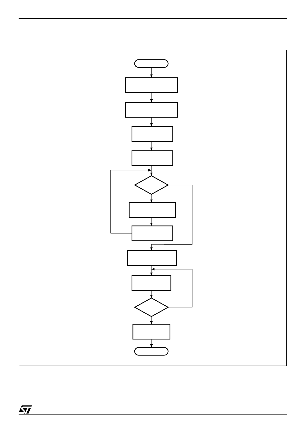
APPENDIX C. FLOW CHARTS
Figure 25. Write to Buffer and Program Flowchart and Pseudo Code
Start
Write to Buffer E8h
Command, Block Address
M58LW128A, M58LW128B
Note 1: N+1 is number of Words or Double
Words to be programmed
Note 2: Next Program Address must
have same A5-A22.
(1)
Write N
Block Address
Write Buffer Data,
Start Address
Write Next Buffer Data,
Next Program Address
X = X + 1
Program Buffer to Flash
Confirm D0h
,
X = 0
X = N
NO
YES
(2)
Note 3: A full Status Register Check must be
done to check the program operation's
success.
Read Status
Register
b7 = 1
YES
Full Status
Register Check
End
NO
(3)
AI03635
57/65

M58LW128A, M58LW128B
Figure 26. Program Suspend & Resume Flowchart and Pseudo Code
Start
Write B0h
Write 70h
Read Status
Register
b7 = 1
YES
b2 = 1
YES
Write FFh
Read data from
another block
Write D0h
Program Continues
NO
NO
Program Complete
Write FFh
Read Data
Program/Erase Suspend Command:
– write B0h
– write 70h
do:
– read status register
while b7 = 1
If b2 = 0, Program completed
Read Memory Array instruction:
– write FFh
– one or more data reads
from other blocks
Program Erase Resume Command:
– write D0h
to resume erasure
– if the program operation completed
then this is not necessary. The device
returns to Read Array as normal
(as if the Program/Erase Suspend
command was not issued).
58/65
AI00612

Figure 27. Erase Flowchart and Pseudo Code
Start
M58LW128A, M58LW128B
Write 20h
Write D0h to
Block Address
Read Status
Register
b7 = 1
YES
b3 = 0
YES
b4, b5 = 1,1
NO
b1 = 0
YES
NO
NO
YES
NO
NO
Suspend
VPP Invalid
Sequence Error
Erase to Protected
Block Error
YES
Error (1)
Command
Suspend
Loop
Erase command:
– write 20h
– write D0h to Block Address
(A12-A17)
(memory enters read Status
Register after the Erase command)
do:
– read status register
– if Program/Erase Suspend command
given execute suspend erase loop
while b7 = 1
If b3 = 1, VPP invalid error:
– error handler
If b4, b5 = 1,1 Command Sequence error:
– error handler
If b1 = 1, Erase to Protected Block Error:
– error handler
b5 = 0
End
Note: 1. If an error is found, the Status Regist er must be cleared (Cl ear Status Regist er Command) before further P rogram or Erase oper-
ations.
NO
YES
Erase
Error (1)
If b5 = 1, Erase error:
– error handler
AI00613C
59/65

M58LW128A, M58LW128B
Figure 28. Erase Suspend & Resume Flowchart and Pseudo Code
Start
Write B0h
Write 70h
Read Status
Register
b7 = 1
YES
b6 = 1
YES
Write FFh
Read data from
another block
or Program
Write D0h
Erase Continues
NO
NO
Erase Complete
Write FFh
Read Data
Program/Erase Suspend Command:
– write B0h
– write 70h
do:
– read status register
while b7 = 1
If b6 = 0, Erase completed
Read Memory Array command:
– write FFh
– one o more data reads
from other blocks
Program/Erase Resume command:
– write D0h to resume the Erase
operation
– if the Program operation completed
then this is not necessary. The device
returns to Read mode as normal
(as if the Program/Erase suspend
was not issued).
60/65
AI00615

M58LW128A, M58LW128B
Figure 29. Command Interface and Program E rase Con trolle r Flowchart (a)
WAIT FOR
COMMAND
WRITE
NO
90h
YES
READ
SIGNATURE
98h
YES
CFI
QUERY
NO
70h
YES
READ
STATUS
NO
50h
CLEAR
STATUS
PROGRAM
COMMAND
ERROR
YES
NO
NO
PROGRAM
BUFFER
E8h
LOAD
D0h
C
YES
YES
NO
20h
YES
ERASE
SET-UP
D0h
YES
A
READ
ARRAY
NO
(1)
NO
FFh
YES
NO
ERASE
COMMAND
ERROR
B
Note 1. The Erase command (20h) can only be issued if the flash is not already in Erase Suspend.
AI03618
61/65

M58LW128A, M58LW128B
Figure 30. Command Interface and Program E rase Con trolle r Flowchart (b)
WAIT FOR
COMMAND
WRITE
B
READ
ARRAY
YES
FFh
NO
ERASE
SUSPENDED
YES
NO
READ
STATUS
YES
YES
A
ERASE
READY
?
NO
B0h
YES
ERASE
SUSPEND
READY
?
NO
READ
STATUS
(READ STATUS)
Program/Erase Controller
Status bit in the Status
Register
NO
READ
STATUS
PROGRAM
COMMAND
ERROR
READ
STATUS
READ
SIGNATURE
CFI
QUERY
PROGRAM
BUFFER
LOAD
NO
D0h
YES
c
YES
YES
YES
YES
70h
NO
90h
NO
98h
NO
E8h
NO
D0h
READ
ARRAY
NO
YES
READ
STATUS
(ERASE RESUME)
AI03619
62/65

M58LW128A, M58LW128B
Figure 31. Command Interface and Program E rase Con trolle r Flowchart (c)
B
C
WAIT FOR
COMMAND
WRITE
READ
STATUS
YES
PROGRAM
SUSPENDED
YES
READ
ARRAY
FFh
NO
70h
YES
NO
NO
READ
STATUS
YES
YES
PROGRAM
READY
?
NO
B0h
YES
PROGRAM
SUSPEND
READY
?
NO
READ
STATUS
(READ STATUS)
Program/Erase Controller
Status bit in the Status
Register
NO
READ
STATUS
READ
SIGNATURE
CFI
QUERY
READ
ARRAY
YES
YES
NO
90h
98h
D0h
NO
NO
YES
READ
STATUS
(PROGRAM RESUME)
AI00618
63/65

M58LW128A, M58LW128B
REVISION HIST ORY
Table 35. Document Revision History
Date Version Revision Details
07-Dec-2001 -01 First Issue.
Version number format modified (major.minor),
Revision History moved to end of document.
16-Dec-2002 1.1
25-Feb-2003 1.2
M58LW128A and M58LW128B device codes changed; Manufacturer code clarified.
Table 10, Read Electronic Signature, clarified.
Data Retention information added to Table 11, Program, Erase Times and Program
Erase Endurance Cycles. CFI information (Table 30, Table 31, Table 32 and Table
34) clarified. Document Status changed to Preliminary Data.
OTP size corrected. Word program not supported clarified in Table 31, CFI - Device
Voltage and Timing Specification and DQ15-DQ0 values changed to 0000h for
addresses 1Fh and 23h. Number (n-1) of Erase Blocks of identical size corrected in
Table 32, Device Geometry Definition. ASCII for 0049h corrected in Table 34,
Extended Query information.
E and F lead-free packing options added to Table 27, Ordering Information Scheme.
64/65

M58LW128A, M58LW128B
Information furnished is believed to be ac curate and reli able. Howev er, STMicroel ectronics assumes no responsibilit y for the consequence s
of use of such information nor for any infringement of patents or other rights of third parties which may result from its use. No license is granted
by implic ation or otherwise under any patent or patent rights of STMi croelectr onics. Specifications mentioned in thi s publicati on are subject
to change without notice. This publication supersedes and replaces all information previously supplied. STMicroelectronics products are not
authorized for use as cri tical comp onents in life support dev i ces or systems wi t hout express written ap proval of STMi croelect ro nics.
The ST log o i s registered trademark of STMicroelectronics
All other nam es are the pro perty of their respective owners
© 2003 STMicroelectronics - All Rights Reserved
STMicroelectron ic s group of com panies
India - Israel - Italy - Japan - Malaysia - Malta - Morocc o - S in gapore - Spain - Sweden - S wi t zerland - Uni t ed Kingdom - United States.
Austra lia - Brazil - Can ada - China - Finl and - France - Germany - Hong Kong -
www.st.com
65/65
 Loading...