

64 Mbit (x16 and x16/x32, Block Erase)
■ M58LW064A x16 organisation,
■ M58LW064B x16/x32 selectable
■ MULTI-BIT CELL for HIGH DENSITY andLOW
COST
■ SUPPLY VOLTAGE
–VDD= 2.7V to 3.6V Supply Voltage
–V
■ PIPELINED SYNCHRONOUS BURST
INTERFACE
■ SYNCHRONOUS/ASYNCHRONOUS READ
– Synchronous Burst read
– Asynchronous Random and Latch Enabled
■ ACCESS TIME
– Synchronous Burst Read up to 66MHz
– Asynchronous Page Mode Read 150/25ns,
■ PROGRAMMING TIME
– 16 Word or 8 Double-Word Write Buffer
– 12us Word effective programming time
■ MEMORY BLOCKS
– 64 Equal blocks of 1 Mbit
■ ELECTRONIC SIGNATURE
– Manufacturer Code: 20h
– Device Code M58LW064A:17h
– Device Code M58LW064B:14h
= 2.7V to 3.6V or 1.8V to 2.5V
DDQ
Input/Output Supply Voltage
Controlled Read, with Page Read
Random Read 150ns
M58LW064A
M58LW064B
Low Voltage Flash Memories
PRODUCT PREVIEW
86
1
TSOP56 (NF)
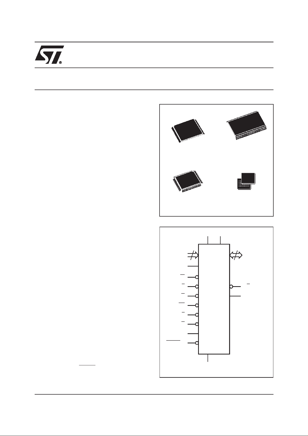
Figure 1. Logic Diagram
V
DD
22
A1-A22
V
PP
W
E
G
RP
M58LW064A
M58LW064B
V
DDQ
TSOP86 II (NH)
FBGA
LBGA54 (ZA)PQFP80 (T)
32
DQ0-DQ31
RB
R
DESCRIPTION
The M58LW064 is a non-volatile Flash memory
that may be erased electrically at the block level
and programmed in-system on a 16 Word or 8
Double-Word basis usinga2.7V to 3.6V supply for
the circuit and a supply down to 1.8V for the Input
WORD
L
B
K
(1)
and Output buffers. TheM58LW064A is organised
as 4M by 16 bit. The M58LW064B has 4M by 16
bit or 2M by 32 bit organisation selectable by the
Word Organisation WORD input. Both devices are
V
SS
internally configured as 64 blocks of 1 Mbit each.
Note: 1. Only on M58LW064B.
May 2000
This is preliminary information on a new product now in development. Details are subject to change without notice.
AI03223
1/53
M58LW064A, M58LW064B
Table 1. Signal Names
A1-A22 Address Inputs x16 Organisation
A2-A22 Address inputs x32 Organisation
Data Input/Output x16 and x32
Organisation Command Input,
DQ0-DQ7
DQ8-DQ15
DQ16-DQ31 Data Input/Output x32 Organisation
B Burst Address Advance
E Chip Enable
G Output Enable
K Burst Clock
L Latch Enable
R Valid Data Ready (open drain output)
RB Ready/Busy (open drain output)
RP Reset/Power-down
V
PP
W Write Enable
WORD Word Organisation (M58LW064B only)
V
DD
V
DDQ
V
SS
NC No internal connection
DU Don’t Use (internally connected)
Electronic Signature Output, Block
Protection Ststus Output, Status
Register Output
Data Input/Output x16 and x32
Organisation
Program/Erase Enable
Supply Voltage
Input/Output Supply Voltage
Ground
The devices support Asynchronous Random and
Latch EnableControlledRead withPage mode as
well as Synchronous Burst Read with a configurable burst. They also support pipelined synchronous Burst Read. Writing is Asynchronous or
Asynchronous Latch Enable Controlled.
The configurablesynchronous burst read interface
allows a high data transfer rate controlled by the
Burst Clock K signal. It is capable of bursting fixed
or unlimited lengths of data. The burst type, latency and length are configurable and can be easily
adapted to a large variety of system clockfrequencies and microprocessors. A 16 Word or 8DoubleWord Write Buffer improves effective programming speed by up to 20 times when data is programmed in full buffer increments. Effective Word
programming takes typically 12µs. The array matrix organisation allows each block to be erased
and reprogrammed without affecting other blocks.
Program and Erase operations can be suspended
in order to perform either Read or Program in any
other block and then resumed. All blocks are protected against spurious programming and erase
cycles at power-up. Any block can be separately
protected at any time. The block protection bits
can also be deleted, this is executed as one sequence for all blocks simultaneously. Block protection can be temporarily disabled. Each block can
be programmed and erased over 100,000 cycles.
Block erase is performed in typically 1 second.
An internal Command Interface (C.I.) decodes Instructions to access/modify the memory content.
The Program/Erase Controller (P/E.C.) automatically executes the algorithms taking care of the
timings required by the program and erase operations. Verification is internally performed and a
Status Register tracks thestatus of the operations.
The Ready/Busy output RB indicates the completion of operations.
Instructions are written to the memory through the
Command Interface (C.I.) using standard microprocessor write timings. The device supports the
Common Flash Interface (CFI) command set definition.
A Reset/Power-down mode is entered when the
RP input is Low. In this modethe power consumption is lower than in the normalstandbymode, the
device is write protected and both the Status and
the Burst Configuration Registers are cleared. A
recovery time is required when the RP input goes
High.
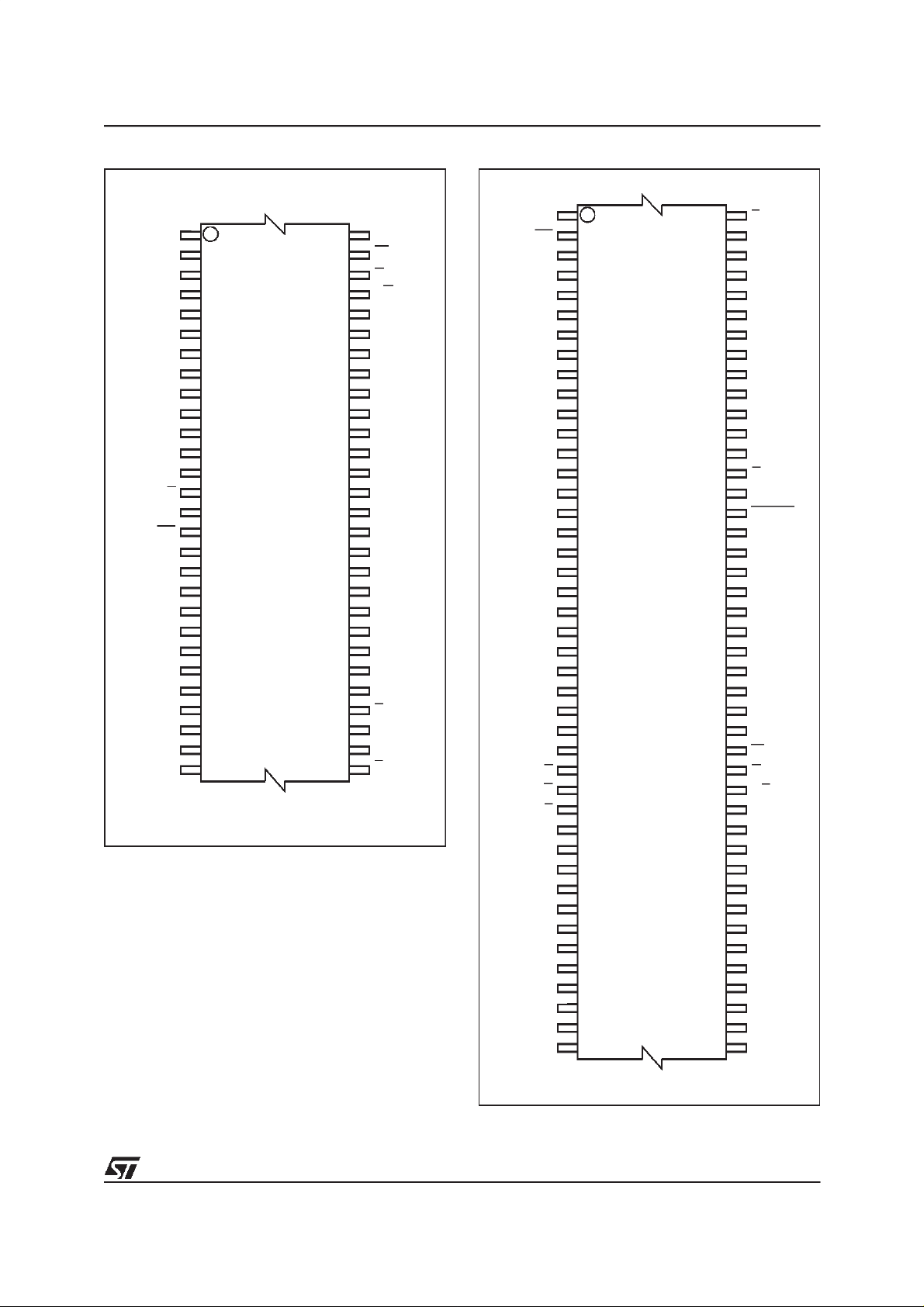
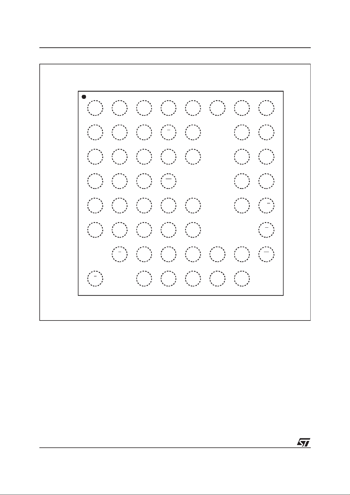
The device is offered in various package versions,
TSOP56 (14 x 20 mm), TSOP86 Type II (11.76 x
22.22 mm) and LBGA54 1mm ball pitch for the
M58LW064A and PQFP80 for the M58LW064B.
2/53
M58LW064A, M58LW064B
Figure 2. TSOP56 Connections
A22
A21
A20
A19
A18
A17
A16
V
A15
A14
A13
A12
V
A11
A10
V
DD
PP
RP
SS
1
R
14
E
M58LW064A
15
A9
A8
A7
A6
A5
A4
A3
A2
28 29
A1
AI03224
56
43
42
NC
W
G
RB
DQ15
DQ7
DQ14
DQ6
V
SS
DQ13
DQ5
DQ12
DQ4
V
DDQ
V
SS
DQ11
DQ3
DQ10
DQ2
V
DD
DQ9
DQ1
DQ8
DQ0
B
K
NC
L
Figure 3. TSOP86 Type II Connections
V
PP
RP
A11
A10
A9
A8
V
SS
SS
A7
A6
A5
A4
A3
A2
A1
NC
NC
NC
NC
NC
DQ16
DQ24
DQ25
DQ18
DQ26
DQ19
DQ27
DQ0
DQ8
DQ1
DQ9
V
DD
V
DD
DQ2
DQ10
DQ3
DQ11
V
SS
V
SS
1
21
M58LW064A
22
L
K
B
43 44
86
66
65
AI03634
E
A12
A13
A14
A15
V
DD
V
DD
A16V
A17
A18
A19
A20
A21
R
A22
WORD
NC
NC
NC
DQ31
DQ23
DQ30
DQ22DQ17
DQ29
DQ21
DQ28
DQ20
W
G
RB
DQ15
DQ7
DQ14
DQ6
V
SS
V
SS
DQ13
DQ5
DQ12
DQ4
V
DDQ
V
DDQ
V
DDQ
3/53
M58LW064A, M58LW064B
Figure 4. LBGA Connections for M58LW064A (Top view through package)
87654321
A
B RA19A2
C
D A16
E
F
G
A1
A4 A5
K
A6 V
V
SS
A7A3
DQ0
A8
A10 A12
A11
DQ10
DQ2B
PP
EA9
RP
DDQ
A13
A14
A15
DQ5V
V
DD
DQ6
A20
DQ15 R/BDQ9DQ8 DQ1 DQ4DQ3
DQ14
A22A18
A21
A17
GDQ12DQ11
W
4/53
H
L
V
DD
V
SS
DQ13
V
SS
DQ7
AI03536
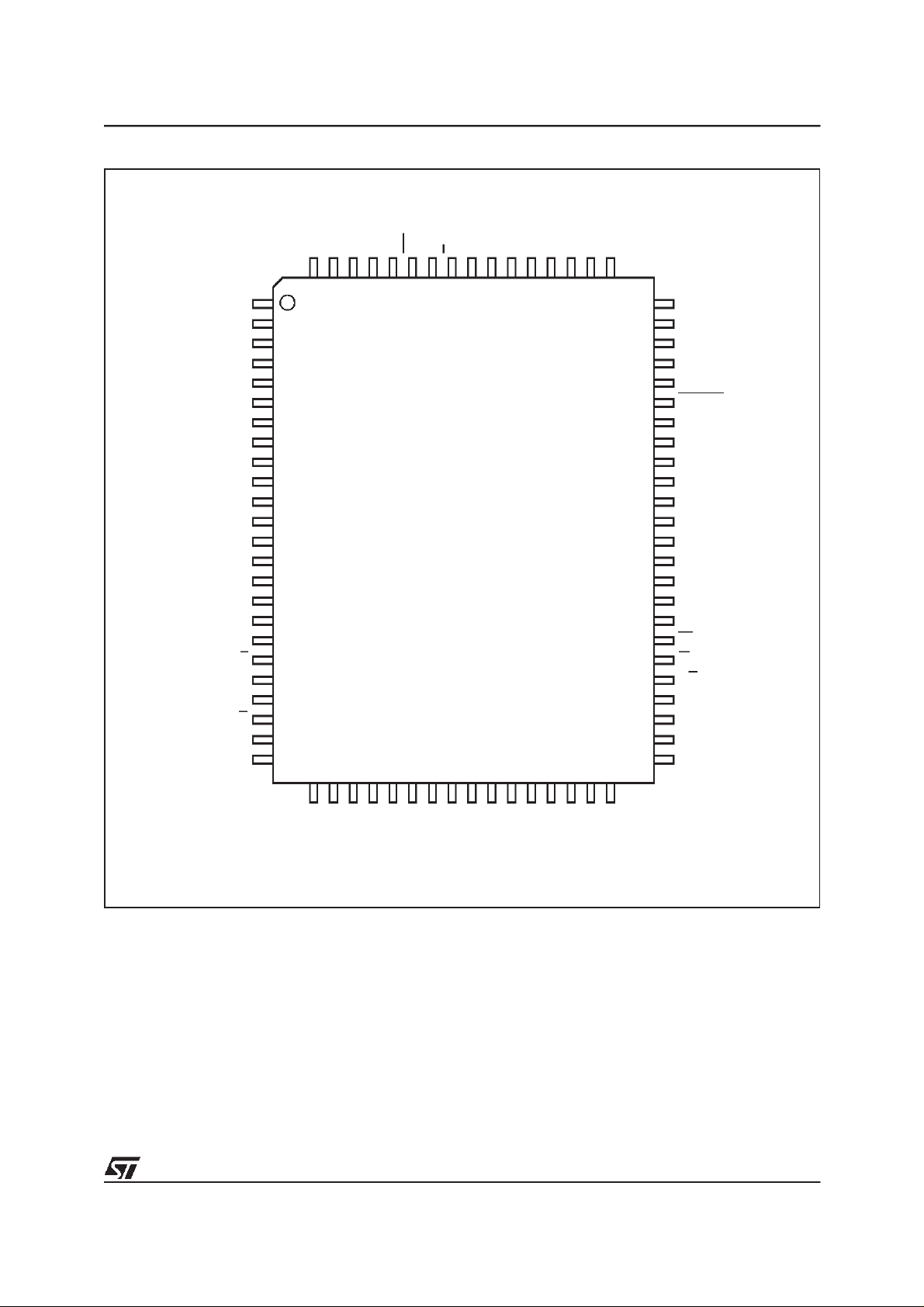
Figure 5. PQFP Connections
M58LW064A, M58LW064B
A7
A6
A5
A4
A3
A2
A1
NC
NC
NC
DQ16
DQ24
DQ17
DQ25
DQ18
DQ26
DQ19
DQ27
NC
DQ0
DQ8
SS
A9
A10
A8
V
1
A11
RP
V
PP
73
A13
E
A12
A14
A15
12 M58LW064B 53
L
K
B
32
DD
V
A16
A17
A18
A19
A20
A21
R
A22
WORD
NC
NC
NC
DQ31
DQ23
DQ30
DQ22
DQ29
DQ21
DQ28
DQ20
W
G
RB
DQ15
DQ7
DQ14
DQ6
DQ1
DQ9
DD
V
DQ2
DQ3
DQ10
SS
V
DQ11
DDQ
V
DDQ
V
DQ4
DQ5
DQ12
VSSV
DQ13
SS
AI03546
5/53
M58LW064A, M58LW064B
Table 2. Absolute Maximum Ratings
(1)
Symbol Parameter Value Unit
Grade 1 0 to 70 °C
T
A
T
BIAS
T
STG
V
IO
V
DD,VDDQ
V
HH
Note: 1. Except for the rating ”Operating Temperature Range”, stresses above those listed in the Table ”Absolute Maximum Ratings” may
cause permanent damage to the device. These are stress ratings only and operation of the device at these or any other conditions
above those indicated in the Operating sections of this specification is not implied. Exposure to Absolute Maximum Rating conditions for extended periods may affect device reliability. Refer also to theSTMicroelectronics SURE Program and otherrelevant quality documents.
2. Cumulative time at a high voltage level of 10V should not exceed 80 hours on RP pin.
Ambient Operating Temperature
Grade 6 –40 to 85
Temperature Under Bias –40 to 125 °C
Storage Temperature –55 to 150 °C
Input or Output Voltage
–0.6 to V
DDQ
+0.6
V
Supply Voltage –0.6 to 5.0 V
RP Hardware Block Unlock Voltage
–0.6 to 10
(2)
V
6/53
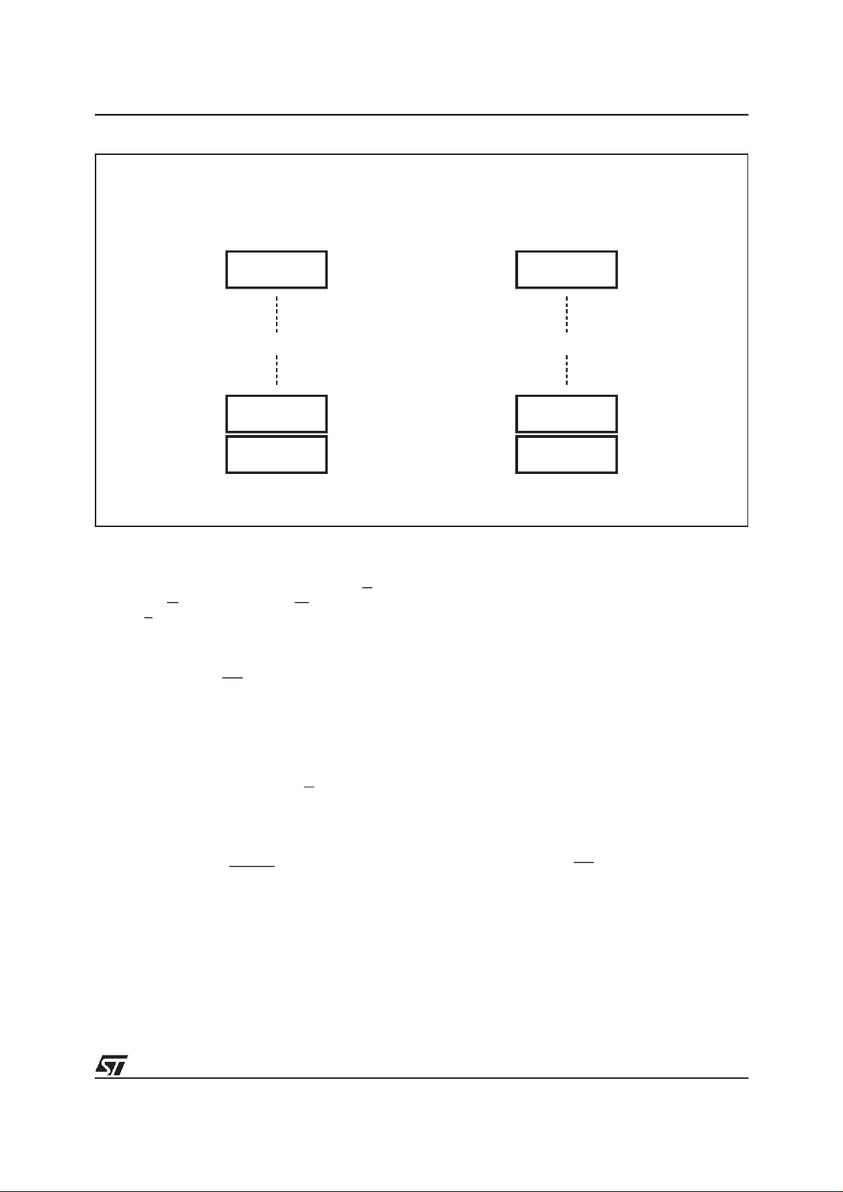
Figure 6. Memory Map
M58LW064A, M58LW064B
M58LW064A,
Word (x16)
Address lines A1-A22
3FFFFFh
3F0000h
01FFFFh
010000h
00FFFFh
000000h
M58LW064B
Organisation
1Mbit or
64 KWords
x64
1Mbit or
64 KWords
1Mbit or
64 KWords
ORGANISATION
Memory control is provided by Chip Enable E,Output Enable G and Write Enable W inputs. A Latch
Enable L input latches an address for both Read
and Write operations. The Burst Clock K and the
Burst Address Advance B inputs synchronize the
memory to the microprocessor during burst read.
Reset/Power-down RP is used to reset all the
memory circuitry, excluding the block protection
bits, andtosetthe chip indeep power down mode.
Erase and Program operations are controlled by
an internal Program/Erase Controller (P/E.C.). A
Status Register data output on DQ7 provides a
Ready/Busy signal to indicate the state of the P/
E.C. operations. A Ready/Busy RB output also indicates the completion of the internal algorithms. A
Valid Data Ready R output indicates the memory
data output valid status during the synchronous
burst mode operations.
A Word Organisation WORD input selects the x16
or x32data width for the M58LW064B. For the x16
only organisation of the M58LW064A or the x16
organisation of the M58LW064B theaddress lines
are A1-A22 and the Data Input/Output is on DQ0DQ15. For the x32 organisation of the
M58LW064B the address lines are A2-A22 and
the Data Input/Output is DQ0-DQ31.
Double-Word (x32)
1FFFFFh
1F8000h
00FFFFh
008000h
007FFFh
000000h
M58LW064B
Address lines
(A1 is Don’t Care)
32 KDouble-Words
32 KDouble-Words
32 KDouble-Words
Organisation
A2-A22
1Mbit or
x64
1Mbit or
1Mbit or
AI03228
MEMORY BLOCKS
The device has a uniform block architecture with
an array of 64 separate blocks of 1Mbit each. The
memory features a software erase suspend of a
block allowing read or programming within any
other block. A suspended erase operation can be
resumed to complete block erasure. A program
suspend operation on a block allows reading only
within any other block. A suspend program operation can be resumedto complete programming.At
any moment of the sequence the Status Register
indicates the status of the operation.
Each block is erased separately. An Erase or Program operation is managed automatically by the
P/E.C. Individual block protection against Program
or Erase provides additional data security. All
blocks are protected during power-up. A software
instruction is provided to cancel all block protection bits simultaneously in an application and a
higher level input on RP can temporarily disable
the protection mechanism. A software instruction
is provided to allow protection of some or all of the
blocks in an application. All Program or Erase operations are blocked when the Program/Erase Enable input VPPis Low.
7/53
M58LW064A, M58LW064B
BUS OPERATIONS
The following operations can be performed using
the appropriate bus configuration:
Asynchronous
– Read Array
– Read Electronic Signature
– Read Block Protection
– Read Status Register
– Read Query
– Write
– Output Disable
– Standby
– Reset/Power-down
Synchronous
– Address Latch
– Burst Read
– Burst Read Suspend
– Burst Read Interrupt
– Burst Read Resume
– Burst Address Advance
See Tables 3, 4, 5, 6 and 7.
COMMAND INTERFACE
Instructions, made up of Commands written in Cycles, can be given to the Program/Erase Controller
(P/E.C.) by writing to the Command Interface
(C.I.). At power-up or on exit from power down or
if VDDis lower than V
, the Command Interface
LKO
is resetto Read Array. Any incorrect commandwill
reset the device to Read Array. Anyimproper command sequence will cause the Status Register to
report the error condition and the device will default to Read Status Register.
The internal Program/Erase Controller (P/E.C.)
automatically handles all timing and verification of
the Program and Erase operations. The Status
Register information P/ECS on DQ7 can be read
at any time, during programming or erase, to monitor the progress of the operation.
Table 3. Asynchronous Bus Operations
Operation E G W RP L DQ0-DQ31
Read Array
Read Electronic Signature or
Block Protection Status
Read Status
P/E.C. Active
Read Query
Write V
Output Disable
Standby
Reset/Power-down X X X
Note: 1. X = Don’t Care VILor VIH. High = VIHor VHH.
2. ? = need to check with designers - X or V
V
IL
V
IL
V
IL
V
IL
IL
V
IL
V
IH
(1)
V
IL
V
IL
V
IL
V
IL
V
IH
V
IH
X X High X High Z
???
IL
V
IH
V
IH
V
IH
V
IH
V
V
IH
High X Data Output
High X
High X Status Register Output
High X CFI Query Output
High V
IL
High X High Z
V
IL
IL
X High Z
Manufacturer or Device Code
Output Block Protection Status
Data Input
8/53
M58LW064A, M58LW064B
Table 4. Synchronous Burst Read Operations
(1)
Operation E G RP K L B
Address Latch
Burst Read
Burst Read Suspend
Burst Read Interrupt (E)
V
IL
V
IL
V
IL
V
IH
Burst Read Interrupt (RP) X X
Burst Read Resume
Burst Address Advance
No Data Output Burst Address
Advance with valid Data Output
Note: 1. X = Don’t Care, VILor VIH.
2. ? need to check with designers for various X and clock _/ definitions
V
IL
V
IL
V
IL
V
IH
V
IL
V
IH
X
V
IL
V
IH
V
IL
V
IH
V
IH
V
IH
V
IH
V
IL
V
IH
V
IH
V
IH
Table 5. Asynchronous Read Electronic Signature Operation
Code Device E G W A22-A1 A22-A2 DQ7-DQ0
Manufacturer All
M58LW064A
Device
M58LW064B
Note: 1. For M58LW064B, A1 = Dont’Care
(1)
V
IL
V
IL
V
IL
V
IL
V
IL
V
IL
V
V
V
A1-A22
DQ0-DQ31
_/
_/
X
X
V
IL
V
IH
V
IH
V
IH
V
IH
V
IH
V
IH
V
IH
Addess Input
Data Output
High Z
High Z
X X X High Z
_/
_/
_/ V
IH
IH
IH
V
IH
V
IH
IH
00000h 00000h 20h
00001h – 17h
V
IL
V
IL
V
IL
Data Output
High Z
Data Output
– 00001h 14h
Table 6. M58LW064A CFI Block Protection Status Query Operation
(1)
Block Status E G W A1 A2 A3-A16 A17-A22 DQ7-DQ0
Protected
Unprotected
Note: 1. X = Dont’Care, VILor VIH.
V
IL
V
IL
Table 7. M58LW064B CFI Block Protection Status Query Operation
V
IL
V
IL
V
IH
V
IH
V
IH
V
IH
V
IH
V
IH
X Block Address 01h
X Block Address 00h
(1)
Block Status E G W A1 A2 A3 A4-A16 A17-A22 DQ7-DQ0
Protected
Unprotected
Note: 1. X = Dont’Care, VILor VIH.
V
IL
V
IL
V
V
V
IL
IL
IH
V
IH
V
X
V
X
V
IH
IH
IH
V
IH
X Block Address 01h
X Block Address 00h
9/53

M58LW064A, M58LW064B
SIGNAL DESCRIPTIONS
See Figure 1 and Table 1.
Address Inputs (A1-A22). A1 is used to select
between the high and low Word in the x16 configuration of the M58LW064A or B. For the
M58LW064B A1 is not used in the x32 mode.
When Chip Enable E is at VILthe address bus is
used to input addresses for the memory array in
Read mode, or addresses for the data to be programmed, or to input addresses associated with
Commands to be written to the Command Interface. Theaddress latch is transparent when Latch
Enable L is at VIL. The address inputs for the
memory array are latched on the rising edge of
Chip Enable E or Latch Enable L or Write Enable
W, whichever occurs first in a writeoperation. The
address is also internally latched in the command
for an Erase or Program Instruction.
Data Inputs/Outputs (DQ0-DQ31). Input data
for a Write to Buffer andProgram operation andfor
writing Commands to the Command Interface are
latched on the rising edge of Write Enable W or
Chip Enable E, whichever occurs first.
When Chip Enable E and Output Enable G are at
VILdata is output from the Array, the Electronic
Signature - the Manufacturer and the Device code
- the Block Protection status, the CFI Query information or the Status Register.The databus is high
impedance when the device is deselected with
Chip Enable E at VIH, Output Enable Gis at VIHor
RP is at VIL. When the P/E.C. is active the Status
Register content is output on DQ0-DQ7 and DQ8DQ31 are at VIL.
Chip Enable (E). The Chip Enable E input activates the memory control logic, input buffers, decoders and sense amplifiers. Chip Enable E at V
IH
deselects thememory and reduces the power consumption to the standby level.
Output Enable (G). The Output Enable G gates
the outputs through the data output buffers during
a read operation. When Output Enable G is at V
IH
the outputs are high impedance. Output Enable G
can be used to suspend the data output in a burst
read operation.
Write Enable (W). The Write Enable W input
controls writing to the Command Interface, Input
Address and Data latches. Both addresses and
data are latched onthe rising edge of W (see also
Latch Enable L).
Reset/Power-down (RP). The Reset/Power-
down RP input provides a hardware reset of the
memory and power-down functions. Reset/Powerdown of the memory is achieved by pulling RP to
VILfor at least t
. Writing is inhibited to protect
PLPH
data, the Command Interface and the P/E.C. are
reset. The Status Register information is cleared
andpower consumptionis reduced to deep powerdown level. The device acts as deselected, that is
the data outputs are high impedance.
When RP rises to VIH, the device will be available
for new operations after a delay of t
PHQV
and will
be configured by default for Asynchronous Random Read. The minimum delay required toaccess
the Command Interface by a write cycle is t
PHWL
If the RP input is activated during a Block Erase, a
Write to Buffer and Program ora Block Protect/Unprotect operation the cycle is aborted and data is
altered and may be corrupted. The Ready/Busy
output RB may remain low for a maximum time of
t
PLPH+tPHRH
beyond the completion of the Reset/
Power-down RP pulse.
Applying the highervoltage VHHtothe Reset/Pow-
er-down input RP temporarily unprotects and enables Erase and Program operations on allblocks.
Thus it acts as a hardware block unprotect input.
In an application, it is recommended to associate
RP to the reset signal of the microprocessor. Otherwise, if a reset operation occurs while the device
is performing an Erase or Program cycle, the
Flash memory may output the Status Register information instead of being re-initialized to the default Asynchronous Random Read.
Latch Enable (L). Latch Enable L latches the address bits A1-A22 on its rising edge for the Asynchronous Latch Enable Controlled Read or Write,
or Synchronous Burst Read operations. The address latch is transparent when Latch Enable L is
at VIL. Latch Enable Lmust remain at VILforAsynchronous Random Read and Write operations.
.
10/53

M58LW064A, M58LW064B
Burst Clock (K). The Burst Clock K is used only
in burst mode. It is the fundamental synchronous
signal that allows internal latching of the address
from the address bus, together with Latch Enable
L; increment of the internal address counter in association with Burst Address Advance B;and to indicate valid data on the external data bus. All
these operations are synchronously controlled on
the valid edge of the Burst Clock K, which can be
selected to be the rising or falling edge depending
on the definition in the Burst Configuration Register.
For Asynchronous Read or Write, the Burst Clock
K input level is Don’tCare. For Synchronous Burst
Read the address is latched on the first valid clock
edge when Latch Enable L is at VIL, or the rising
edge of Latch Enable L, whichever occurs first.
Burst Address Advance (B). Burst Address Advance Benables increment of the internal address
counter when it falls to VILduring Synchronous
Burst Read. It is sampled on the last valid edge of
the Burst Clock K at the expiry of the X-latency
time. If sampled at VIL, new data will be output on
the next Burst Clock K valid edge (or second next
depending on the definitionin the Burst Configuration Register). If it is at VIHwhensampled, the previous data remains on the Data Outputs. The Burst
Address Advance B may be tied to VIL.
Ready (R). The Valid Data Ready R is an output
signal used during Synchronous Burst Read. It indicates, at the valid clock edge (or one cycle before depending on the definition in the Burst
Configuration Register), if valid data is ready on
the Data Outputs. New Data Outputs are valid if
Valid Data Ready R is at VIH, the previous Data
Outputs remain active if Valid Data Ready R is at
VIL.
In all operations except Burst Read, Valid Data
Ready R is at VIH. It may be tied to other components with the same Valid Data Ready R signal to
create a unique system Ready signal. The Valid
Data Ready R output has an internalpull-up resistor ofaround 1 MΩ powered from V
, designers
DDQ
should use an external pull-up resistor of the correct value to meet the external timing requirements for R going to VIH.
Word Organisation (WORD). The Word Organisation WORD input is present only on the
M58LW064B and selects x16 or x32 organisation.
The WORD input selects the data width as Word
wide (x16) or Double-Word wide (x32). When
WORD is at VIL, Word-wide x16 width is selected
and data is read and programmedon DQ0-DQ15,
DQ16-DQ31 are at high impedance and A1 is the
LSB address. When WORD is at VIH, the DoubleWord wide x32 width is selected and the data is
read and programmed on DQ0-DQ31, and A2 is
the LSB address.
Ready/Busy (RB). Ready/Busy RB is an opendrain output and gives the internal state of the P/
E.C. When Ready/Busy RB is at VILthe device is
busy with a Program or Erase operation and it will
not accept any additional program or erase instructions except for the Program or Erase Suspend instructions. When a Program or Erase
Suspend is given the RB signal rises to VIH, after
a latency time, to indicate that the Command Interface is ready for a new instruction. When RB is at
VIH, the device is ready for any Read, Program or
Erase operation. Ready/Busy RB is also at V
IH
whenthe memory isin Erase/Program Suspend or
Standby modes.
Program/Erase Enable (VPP). Program/Erase
Enable VPPautomatically protects all blocks from
programming or erasure when at VIL.
Supply Voltage (VDD). The Supply Voltage V
DD
is the main power supply for all operations (Read,
Program and Erase).
Input/Output Supply Voltage (V
put/Output Supply Voltage V
DDQ
). The In-
DDQ
is the Input and
Output buffer power supply for all operations
(Read, Program and Erase).
Ground (VSS). Ground VSSisthe reference for all
the voltage measurements.
11/53

M58LW064A, M58LW064B
DEVICE OPERATIONS
See Tables 5, 6, 7 and 10.
Address Latch. An address is latched on the ris-
ing edge of the Latch Enable L input for Asynchronous Latch Enable Controlled Read. For
Asynchrouns Latch Enable Controlled Write, the
address is latched on the rising edge of Chip Enable E, Write Enable W or Latch Enable L, whichever occurs first.
For Synchronous Burst Read the address is
latched on the first valid Burst Clock K edge when
Latch Enable L is at Low, or on the rising edge of
Latch Enable L, whichever occurs first.
Asynchronous Random Read. Asynchronous
Random Read outputs the contents of the Array.
Both Chip Enable E andOutput Enable G must be
Low in order to read the output of the memory.
By first writing the appropriate Instruction, the
Electronic Signature (RSIG), the Status Register
(RSR), the Read Query Instruction (RCFI) or the
Block Protection Status (RSIG) can be read.
Asynchronous Random Read is the default read
mode which the device enters on power-up or on
return fromReset/Power-down.
Asynchronous Page Read. Asynchronous
Page Read may be used for Random or Latch Enable Controlled Reads of the Array, which are performed independent of the Burst Clock signal. A
page has a size of 4 Words or 2 Double-Words
and is addressed by the address inputs A1 and A2
in the x16, or A2 only in the x32 organisation. Data
is read internally and stored in the Page Buffer.
The page read starts when both Chip Enable E
and Output Enable G are Low. The first data is internally read and is output after the normal access
time t
. Successive Words or Double-Words
AVQV
can be read with a much reduced access time of
t
AVQV1
by changing only the low address bits.
Synchronous Burst Read. The memory supports different types of burst access using a Burst
Configuration Register to configure the burst type,
length and latency.
In continuous burst read, one burst read operation
can access the entire memory sequentially by
keeping the Burst Address Advance B Low for the
appropriate number of clock cycles. At the end of
the memory address space the burst read restarts
from the beginning at address 000000h.
Synchronous Burst Read is activated when the
Burst Clock K input is clocking and Chip Enable E
is Low. The burst start address is latched and
loaded into the internal Burst Address Counter on
the valid Burst Clock K edge (rising or falling depending on the M6 bit value for the Burst Clock
Edge Configuration in the Burst Configuration
Register) when Latch Enable Lis Low, orupon the
rising edge of Latch Enable L when the Burst
Clock K is valid. After an initial memory latency
time, the memory outputs data each clock cycle
(or two clock cycles depending onM9 bit value defined in the Burst Configuration Register). The
Burst Address Advance B input controls the memory burst output. The second burst output is on the
next clock valid edge after the Burst Address Advance B has been pulled Low.
The Valid Data Ready output signal R monitors if
the memory burst boundary is exceeded and the
Burst Controller of the microprocessor needs to insert wait states. When Valid Data Ready R is Low
on the active clock edge, no new data is available
and the memory does not increment the internal
address counter at the active clock edge even if
Burst Address Advance B is Low.
Synchronous Burst Read will be suspended when
Burst Address Advance B is High. The Valid Data
Ready signal R may be configured (by bit M8 of
Burst Configuration Register) to be valid immediately at the valid clock edge or one data cyclebefore the valid clock edge.
To increase the data throughput the device has
been built with an internal pipelined architecture
allowing the user to enter a burst read input command and the next starting address location to be
read while the device is filling the output data bus
with its current burst content. This pipelined structure is intended to produce no wait-states on the
output data bus for successive burst read mode
operations.
Asynchronous and Latch Enable Controlled
Write. Asynchronous Write is used to give com-
mands to the Command Interface for Instructions
tothe memory or to latch addressesand input data
to be programmed. To perform any Instruction the
Command Interface is activated starting with a
write cycle. A write cycle is also required give the
Instruction to clear the Status Register information. Two write cycles are needed to define the
Block Erase and the Write to Buffer and Program
Instructions. The first write cycle defines the Instruction selection and the second indicates the
appropriate block address to be erased for the
Block Erase instruction, or the address locations to
program with the number of Words or DoubleWords in the Write to Buffer and Program Instruction.
An Asynchronous Write is initiated when Chip Enable E, Write Enable W and Latch Enable L are
Low with Output Enable G High. Commands and
Input Data are latched on the rising edge of Chip
Enable E or Write Enable W, whichever occurs
first. For an Asynchronous Latch Enable Controlled Write the address is latched on the rising
edge of Latch Enable L, Write Enable W or Chip
Enable E, whichever occurs first.
12/53

M58LW064A, M58LW064B
Data to be programmed in the array is internally
latched inthe Write Bufferbefore theprogramming
operation starts and a minimum of 4 Words or 2
Double-Words need to be programmed in the
same sequence and must be contained in the
same address location boundary defined by A1 to
A2 for the x16 and A2 for the x32 organisation.
Write operations are asynchronous and the Burst
Clock signal K is ignored during a write operation.
Output Disable. The data outputs are high impedance when the Output Enable G is High.
Standby. The memory is in standby when Chip
Enable E goes High and the P/E.C. is idle. The
power consumption is reduced tothe standby level
and the outputs are high impedance, independent
of the Output Enable G or Write Enable W inputs.
Automatic Low Power. After a short time of bus
inactivity (no Chip Enable E, Latch Enable L or Address transitions) the chip automatically enters a
pseudo-standby mode where consumption is reduced to the Automatic Low Power standby value,
while theoutputs may still drive the bus. The Automatic Low Power feature is available only for
Asynchronous Read.
Power-down. The memory is in Power-down
when Reset/Power-down RP is Low. The power
consumption is reduced to the power-down level
and the outputs are high impedance, independent
of the Chip Enable E, Output Enable G or Write
Enable W inputs.
Electronic Signature. Two codes identifying the
manufacturer and the device can be read from the
memory allowing programming equipment or applications to automatically match their interface to
the characteristics of the memory. The Electronic
Signature is output by givingthe RSIG Instruction.
The manufacturer code is output when all the Address inputs are Low. The device code is output
when A1 (M58LW064A) or A2 (M58LW064B) input is High, the other pins A3-A22 must be Low.
The codes are output on DQ0-DQ7. A return to
Read mode is achieved by writing the Read Array
instruction.
INITIALIZATION
The device must be powered up and initialized in
a predefined manner. Procedures other than
specified may result in undefined operation.
Power should be applied simultaneously to V
and V
with the RP input held Low. When the
DDQ
DD
supplies are stable RP is taken High. The Output
Enable G, Chip Enable E and Write Enable W inputs should also be held High during power-up.
The memory will be ready to accept the first Instruction after the power-up time t
. The device
PUR
is automatically configured for Asynchronous Random Read at power-up or after leaving Reset/
Power-down.
BURST CONFIGURATION REGISTER
See Tables 8, 9, 10 and 11.
The Synchronous Burst Read, Asynchronous
Random Read, Asynchronous Latch Enable Controlled Read are selected using the Burst Configuration Register.
For Synchronous Read the register defines the X
and Y Latencies, Valid Data Ready signal timing,
Burst Type, Valid Clock Edge and Burst Length.
The Burst Configuration Register is programmed
usingthe SetBurst Configuration Register (SBCR)
Instruction and will retain the stored information
until it is programmed again or the device is reset
or goes into the Reset/Power-down.
The Burst Configuration Register bits M2-M0
specify the burst length (1, 2, 4, 8 or continuous);
bit M3 specifies Asynchronous Random Read or
Asynchronous Latch Enable Controlled Read; bits
M4and M5 are not used; bit M6 specifies the rising
or falling burst clock edge as valid; bit M7 specifies
the burst type (Sequential or Interleaved); M8
specifies the Valid Data Ready output period; bit
M9 specifies the Y-latency; bit M10 is not used;
M14-M11 specify the X-latency; and bit M15 selects between Synchronous Burst Read or Asynchronous Read. M10, M5 and M4 are reserved for
future use.
M15 Read Select
The device features three kinds of read operation:
Asynchronous Random Read, Asynchronous
Latch Enable Controlled Read and Synchronous
Burst Read. Page Read may be used in either of
the Asynchronous Read operations.
The Burst Configuration Register bit M15 selects
between Synchronous Burst and Asynchronous
Read.
M14 - M11 and M9 X and Y Latency.
The values of X and Y are used to define the burst
latency for the data sequence. The X-latency defines the number of clock cycles before the output
of the first data from the clock edge that latches
the address. The X-latency can be set from 7 to
16. A value of 7 is only valid for continuous burst.
The Y-latency is the number of clock cycles need-
ed to output the next data from the burst register,
following the first data output. The latency can be
set to 1 or 2 clock cycles.
The minimum X-Latency value to consider depends on the Burst Clock K signal frequency. The
burst performance in terms of frequency is listed in
Table 11 and indicates theminimum X-latencyand
Y-latency values (X.Y.Y.Y) related to the burst
type, burst length and x16 or x32 organisation.
13/53

M58LW064A, M58LW064B
M8 Valid Data Ready R Signal Configuration.
The Valid Data Ready R output signal indicates
when valid data is on the data outputs synchronous with the valid burst clock egde. It can be asserted by the device synchronously with the valid
clock edge or one clock cycle before.
M7 Burst Type.
Accesses within a given burst may be programmed to be either Sequential or Interleaved.
This is referred to as the burst type and is selected
by theBurst Configuration Register M7 bit. The access order within a burst is determined by the
burst length, the burst type and the starting address (See Table 8).
M6 Valid Clock Edge Configuration.
All the synchronous operations such as Burst
Read, Output Data or Ready signal validation can
be synchronized on the valid rising or on the falling
edge of the Burst Clock signal K.
M2 - M0 Burst Length.
Synchronous reads have a programmable burst
length, set using the M2- M0 bits of the Burst Configuration Register. The burst length corresponds
to the maximum number of Words or DoubleWords that can be output. Burst lengths of 1, 2, 4
or 8 are available for both the Sequential and Interleaved burst types, and a continuous burst is
available for the Sequential type. The burst length
of 8 is not available in the x32 configuration.
When a Read command is issued, a block of
Words or Double-Words equal to the burst length
is selected. All accesses for that burst take place
within this block, meaning that the burst wraps
within the burst block if a boundary is reached.
If a Continuous Burst Read has been initiated the
device will output data synchronously. Depending
on the starting address of the read, the device activates the Valid Data Ready R output to indicate
that it needs a delay to complete the internal read
operation before outputing data. If the startingaddress is aligned to a four Word boundary the continuous burst mode will run without activating the
Valid Data Ready R output. If the starting address
is not aligned to a four Word boundary,Valid Data
Ready R is activated at the beginning of the continuous burst read to indicate that the device
needs an internal delay to read the content of the
four successive words in the array.
Pipelined Burst Read.
An overlapping Burst Read operation is possible.
That is, the address and data phases of consecutive synchronous read operations can be overlapped by several clock cycles. This is done by
applying a pulse on Latch Enable Linput to latch a
new address before the completion of the data
output of the current cycle. This reduces or avoids
wait-states in the data output for the burst read
mode. The minimum clock edge number for the
following read sequence must be six before the
last data output of the previous read cycle. The
pipelined burst read mode is available in the x16
organisation for both burst length definitions of
four and eight, and in the x32 organisation for the
burst length of four. It is not possible for a burst
length of one or two.
14/53
Table 8. Burst Type Definition (x16 mode)
Starting Address
Burst Length
2
4
8
(binary)
A3-A2-A1
0-0-0 0-1 0-1
0-0-1 1-0 1-0
0-0-0 0-1-2-3 0-1-2-3
0-0-1 1-2-3-0 1-0-3-2
0-1-0 2-3-0-1 2-3-0-1
0-1-1 3-0-1-2 3-2-1-0
0-0-0 0-1-2-3-4-5-6-7 0-1-2-3-4-5-6-7
0-0-1 1-2-3-4-5-6-7-0 1-0-3-2-5-4-7-6
0-1-0 2-3-4-5-6-7-0-1 2-3-0-1-6-7-4-5
0-1-1 3-4-5-6-7-0-1-2 3-2-1-0-7-6-5-4
1-0-0 4-5-6-7-0-1-2-3 4-5-6-7-0-1-2-3
1-0-1 5-6-7-0-1-2-3-4 5-4-7-6-1-0-3-2
1-1-0 6-7-0-1-2-3-4-5 6-7-4-5-2-3-0-1
1-1-1 7-0-1-2-3-4-5-6 7-6-5-4-3-2-1-0
Sequential
(decimal)
M58LW064A, M58LW064B
Interleaved
(decimal)
Table 9. Burst Type Definition (x32 mode)
Starting Address
Burst Length
2
4
(binary)
A2-A1
0-0 0-1 0-1
0-1 1-0 1-0
0-0 0-1-2-3 0-1-2-3
0-1 1-2-3-0 1-0-3-2
1-0 2-3-0-1 2-3-0-1
1-1 3-0-1-2 3-2-1-0
Sequential
(decimal)
Interleaved
(decimal)
15/53
M58LW064A, M58LW064B
Table 10. Burst Configuration Register
(1)
BCR mode bit Description Value Description
0 Synchronous Burst Read
M15 Read Select
1 Asynchronous Read
0001 Reserved
(5)
(6)
(7)
(8)
M14-M11
M9
X-Latency
Y-Latency
(4)
(4)
0010
0011
7, only for F
8, only for F
0100 9, only for F
0101
0110
1001
1010
1011
1101
10, only for F
11, only for F
12, only for F
13, only for F
14, only for F
16, only for F
= 33MHz
K
= 33MHz
K
= 33MHz
K
= 50MHz
K
= 50MHz
K
= 50MHz
K
= 50MHz
K
= 66MHz
K
= 66MHz
K
0 One Burst Clock cycle
1 Two Burst Clock cycles
0 R valid Low during valid Burst Clock edge
M8 Valid Data Ready
1 R valid Low one data cycle before valid Burst Clock edge
0 Interleaved
M7 Burst Type
1 Sequential
0 Falling Burst Clock edge
M6 Valid Clock Edge
1 Rising Burst Clock edge
0 Random Read
M3 Asynchronous
1 Latch Enable Controlled Read
100 1 Word or Double-Word
101 2 Words or Double-Words
M2-M0
Burst Length
(2)
001 4 Words or Double-Words
010
8 Words or Double-Words
(3)
111 Continuous
Note: 1. The BCR defines both the read mode and the burst configuration.
2. Synchronous burst length is defined as Word or Double-Word, the data bus width depends only on the WORD input.
Asynchronous Page read is two Words or one Double-Word.
3. A burst length of 8 is not available for x32 organisation.
> 50MHz when X-Latency = 10 or 12, Y-Latency = 2 independent of the value of M9.
4. At F
K
= 66MHz when X-Lantency = 14 or 16, Y-Latency = 2 indepedent of the value of M9.
At F
K
5. Latency 7 valid only for continuous burst. Otherwisw Latency = 8.
6. Latency 10 valid only for continuous burst. Otherwisw Latency = 12.
7. Latency 11 valid only for continuous burst. Otherwisw Latency = 12.
8. Latency 14 valid only for continuous burst. Otherwisw Latency = 16.
16/53
 Loading...