

32 Mbit (4Mb x8, 2Mb x16, Uniform Block)
FEATURES SUMMARY
■ WIDE x8 or x16 DATA BUS for HIGH
BANDWIDTH
■ SUPPLY VOLTAGE
= V
–V
DD
and Read operations
■ ACCESS TIME
– Random Read 90ns,110ns
– Page Mode Read 90ns/25ns , 110ns/25 ns
■ PROGRAMMING TIME
– 16 Word Write Buffer
–12µs Word effective programming time
■ 32 UNIFORM 64 KWord/128KByte MEMORY
BLOCKS
■ ENHANCED SECURITY
– Block Protection/ Unprotection
–V
PEN
– 128 bit Protection Register with 64 bit Unique
Code in OTP area
■ PROGRAM and ERASE SUSPEND
■ 128 bit PROTECTION REGISTER
■ COMMON FLASH INTERFACE
■ 100, 000 PROGRAM/ERASE CYCLES per
BLOCK
■ ELECTRONIC SIGNATURE
– Manufacturer Code: 0020h
– Device Code M58LW 032D: 0016h
= 2.7 to 3.6V for Program, Erase
DDQ
signal for Program Erase Enable
M58LW032D
3V Supp l y Fl ash Mem ory
Figure 1. Packages
TSOP56 (N)
14 x 20 mm
TBGA
TBGA64 (ZA)
10 x 13 mm
1/51September 2003

M58LW032D
TABLE OF CONTENTS
SUMMARY DESCRIPTION. . . . . . . . . . . . . . . . . . . . . . . . . . . . . . . . . . . . . . . . . . . . . . . . . . . . . . . . . . . 5
Figure 2. Logic Diagram . . . . . . . . . . . . . . . . . . . . . . . . . . . . . . . . . . . . . . . . . . . . . . . . . . . . . . . . . 6
Table 1. Signal Names . . . . . . . . . . . . . . . . . . . . . . . . . . . . . . . . . . . . . . . . . . . . . . . . . . . . . . . . . . 6
Figure 3. TSOP56 Connections . . . . . . . . . . . . . . . . . . . . . . . . . . . . . . . . . . . . . . . . . . . . . . . . . . . . 7
Figure 4. TBGA64 Connections (Top view through package) . . . . . . . . . . . . . . . . . . . . . . . . . . . . . 8
Figure 5. Block Addresses. . . . . . . . . . . . . . . . . . . . . . . . . . . . . . . . . . . . . . . . . . . . . . . . . . . . . . . . 9
SIGNAL DESCRIPTIONS . . . . . . . . . . . . . . . . . . . . . . . . . . . . . . . . . . . . . . . . . . . . . . . . . . . . . . . . . . . 10
Address Input (A0). . . . . . . . . . . . . . . . . . . . . . . . . . . . . . . . . . . . . . . . . . . . . . . . . . . . . . . . . . . . . . 10
Address Inputs (A1-A21). . . . . . . . . . . . . . . . . . . . . . . . . . . . . . . . . . . . . . . . . . . . . . . . . . . . . . . . . 10
Data Inputs/Outputs (DQ0-DQ15 ). . . . . . . . . . . . . . . . . . . . . . . . . . . . . . . . . . . . . . . . . . . . . . . . . .10
Chip Enables (E0, E1, E2). . . . . . . . . . . . . . . . . . . . . . . . . . . . . . . . . . . . . . . . . . . . . . . . . . . . . . . . 10
Output Enable (G). . . . . . . . . . . . . . . . . . . . . . . . . . . . . . . . . . . . . . . . . . . . . . . . . . . . . . . . . . . . . . 10
Write Enable (W). . . . . . . . . . . . . . . . . . . . . . . . . . . . . . . . . . . . . . . . . . . . . . . . . . . . . . . . . . . . . . .10
Reset/Power-Down (RP). . . . . . . . . . . . . . . . . . . . . . . . . . . . . . . . . . . . . . . . . . . . . . . . . . . . . . . . . 10
Byte/Word Organization Select (BYTE). . . . . . . . . . . . . . . . . . . . . . . . . . . . . . . . . . . . . . . . . . . . . . 10
Status/(Ready/Busy) (STS). . . . . . . . . . . . . . . . . . . . . . . . . . . . . . . . . . . . . . . . . . . . . . . . . . . . . . . 10
Program/Erase Enable (V
Supply Voltage. . . . . . . . . . . . . . . . . . . . . . . . . . . . . . . . . . . . . . . . . . . . . . . . . . . . . . . . . . . . . 11
V
DD
V
Supply Voltage . . . . . . . . . . . . . . . . . . . . . . . . . . . . . . . . . . . . . . . . . . . . . . . . . . . . . . . . . . . . 11
DDQ
V
Ground . . . . . . . . . . . . . . . . . . . . . . . . . . . . . . . . . . . . . . . . . . . . . . . . . . . . . . . . . . . . . . . . . . .11
SS
Ground. . . . . . . . . . . . . . . . . . . . . . . . . . . . . . . . . . . . . . . . . . . . . . . . . . . . . . . . . . . . . . . . . . 11
V
SSQ
Table 2. Device Enable . . . . . . . . . . . . . . . . . . . . . . . . . . . . . . . . . . . . . . . . . . . . . . . . . . . . . . . . . 11
). . . . . . . . . . . . . . . . . . . . . . . . . . . . . . . . . . . . . . . . . . . . . . . . . . . . .11
PEN
BUS OPERATIONS. . . . . . . . . . . . . . . . . . . . . . . . . . . . . . . . . . . . . . . . . . . . . . . . . . . . . . . . . . . . . . . . 12
Bus Read. . . . . . . . . . . . . . . . . . . . . . . . . . . . . . . . . . . . . . . . . . . . . . . . . . . . . . . . . . . . . . . . . . . . . 12
Bus Read. . . . . . . . . . . . . . . . . . . . . . . . . . . . . . . . . . . . . . . . . . . . . . . . . . . . . . . . . . . . . . . . . . . . . 12
Bus Write. . . . . . . . . . . . . . . . . . . . . . . . . . . . . . . . . . . . . . . . . . . . . . . . . . . . . . . . . . . . . . . . . . . . . 12
Output Disable. . . . . . . . . . . . . . . . . . . . . . . . . . . . . . . . . . . . . . . . . . . . . . . . . . . . . . . . . . . . . . . . . 1 2
Power-Down . . . . . . . . . . . . . . . . . . . . . . . . . . . . . . . . . . . . . . . . . . . . . . . . . . . . . . . . . . . . . . . . . . 12
Standby . . . . . . . . . . . . . . . . . . . . . . . . . . . . . . . . . . . . . . . . . . . . . . . . . . . . . . . . . . . . . . . . . . . . . . 12
Table 3. Bus Operations . . . . . . . . . . . . . . . . . . . . . . . . . . . . . . . . . . . . . . . . . . . . . . . . . . . . . . . . 12
READ MODES. . . . . . . . . . . . . . . . . . . . . . . . . . . . . . . . . . . . . . . . . . . . . . . . . . . . . . . . . . . . . . . . . . . . 13
COMMAND INTERFACE . . . . . . . . . . . . . . . . . . . . . . . . . . . . . . . . . . . . . . . . . . . . . . . . . . . . . . . . . . . 14
Read Memory Array Command. . . . . . . . . . . . . . . . . . . . . . . . . . . . . . . . . . . . . . . . . . . . . . . . . . . .14
Read Electronic Signature Command . . . . . . . . . . . . . . . . . . . . . . . . . . . . . . . . . . . . . . . . . . . . . . . 14
Read Query Command. . . . . . . . . . . . . . . . . . . . . . . . . . . . . . . . . . . . . . . . . . . . . . . . . . . . . . . . . . . 1 4
Read Status Register Command. . . . . . . . . . . . . . . . . . . . . . . . . . . . . . . . . . . . . . . . . . . . . . . . . . .14
Clear Status Register Command. . . . . . . . . . . . . . . . . . . . . . . . . . . . . . . . . . . . . . . . . . . . . . . . . . . 14
Block Erase Command . . . . . . . . . . . . . . . . . . . . . . . . . . . . . . . . . . . . . . . . . . . . . . . . . . . . . . . . . . 14
Word/Byte Program Command . . . . . . . . . . . . . . . . . . . . . . . . . . . . . . . . . . . . . . . . . . . . . . . . . . . .14
Write to Buffer and Program Command.. . . . . . . . . . . . . . . . . . . . . . . . . . . . . . . . . . . . . . . . . . . . . 15
2/51

M58LW032D
Program/Erase Suspend Comm and . . . . . . . . . . . . . . . . . . . . . . . . . . . . . . . . . . . . . . . . . . . . . . . . 15
Program/Erase Resume Command . . . . . . . . . . . . . . . . . . . . . . . . . . . . . . . . . . . . . . . . . . . . . . . . 15
Block Protect Command.. . . . . . . . . . . . . . . . . . . . . . . . . . . . . . . . . . . . . . . . . . . . . . . . . . . . . . . . . 15
Blocks Unprotect Command.. . . . . . . . . . . . . . . . . . . . . . . . . . . . . . . . . . . . . . . . . . . . . . . . . . . . . . 16
Protection Register Program Command . . . . . . . . . . . . . . . . . . . . . . . . . . . . . . . . . . . . . . . . . . . . . 16
Configure STS Command . . . . . . . . . . . . . . . . . . . . . . . . . . . . . . . . . . . . . . . . . . . . . . . . . . . . . . . . 16
Table 4. Commands . . . . . . . . . . . . . . . . . . . . . . . . . . . . . . . . . . . . . . . . . . . . . . . . . . . . . . . . . . . 17
Table 5. Configuration Codes . . . . . . . . . . . . . . . . . . . . . . . . . . . . . . . . . . . . . . . . . . . . . . . . . . . . 17
Table 6. Read Electronic Signature. . . . . . . . . . . . . . . . . . . . . . . . . . . . . . . . . . . . . . . . . . . . . . . . 18
Figure 6. Protection Register Memory Map. . . . . . . . . . . . . . . . . . . . . . . . . . . . . . . . . . . . . . . . . . 18
Table 7. Word-Wide Read Protection Register. . . . . . . . . . . . . . . . . . . . . . . . . . . . . . . . . . . . . . . 18
Table 8. Byte-Wide Read Protection Register. . . . . . . . . . . . . . . . . . . . . . . . . . . . . . . . . . . . . . . . 19
Table 9. Program, Erase Times and Program Erase Endurance Cycles . . . . . . . . . . . . . . . . . . . 20
STATUS REGISTER. . . . . . . . . . . . . . . . . . . . . . . . . . . . . . . . . . . . . . . . . . . . . . . . . . . . . . . . . . . . . . . 21
Program/Erase Controller Status (SR7) . . . . . . . . . . . . . . . . . . . . . . . . . . . . . . . . . . . . . . . . . . . . . 21
Erase Suspend Status (SR6) . . . . . . . . . . . . . . . . . . . . . . . . . . . . . . . . . . . . . . . . . . . . . . . . . . . . . 21
Erase Status (SR5) . . . . . . . . . . . . . . . . . . . . . . . . . . . . . . . . . . . . . . . . . . . . . . . . . . . . . . . . . . . . . 21
Program Status (SR4). . . . . . . . . . . . . . . . . . . . . . . . . . . . . . . . . . . . . . . . . . . . . . . . . . . . . . . . . . . 21
VPEN Status (SR3). . . . . . . . . . . . . . . . . . . . . . . . . . . . . . . . . . . . . . . . . . . . . . . . . . . . . . . . . . . . . 22
Program Suspend Status (SR2) . . . . . . . . . . . . . . . . . . . . . . . . . . . . . . . . . . . . . . . . . . . . . . . . . . . 22
Block Protection Status (SR1). . . . . . . . . . . . . . . . . . . . . . . . . . . . . . . . . . . . . . . . . . . . . . . . . . . . . 22
Reserved (SR0) . . . . . . . . . . . . . . . . . . . . . . . . . . . . . . . . . . . . . . . . . . . . . . . . . . . . . . . . . . . . . . . . 22
Table 10. Status Register Bits. . . . . . . . . . . . . . . . . . . . . . . . . . . . . . . . . . . . . . . . . . . . . . . . . . . . 23
MAXIMUM RATING. . . . . . . . . . . . . . . . . . . . . . . . . . . . . . . . . . . . . . . . . . . . . . . . . . . . . . . . . . . . . . . . 24
Table 11. Absolute Maximum Ratings. . . . . . . . . . . . . . . . . . . . . . . . . . . . . . . . . . . . . . . . . . . . . . 24
DC and AC PARAMETERS . . . . . . . . . . . . . . . . . . . . . . . . . . . . . . . . . . . . . . . . . . . . . . . . . . . . . . . . . 2 5
Table 12. Operating and AC Measurement Conditions. . . . . . . . . . . . . . . . . . . . . . . . . . . . . . . . . 25
Figure 7. AC Measurement Input Output Waveform . . . . . . . . . . . . . . . . . . . . . . . . . . . . . . . . . . . 25
Figure 8. AC Measurement Load Circuit . . . . . . . . . . . . . . . . . . . . . . . . . . . . . . . . . . . . . . . . . . . . 25
Table 13. Capacitance. . . . . . . . . . . . . . . . . . . . . . . . . . . . . . . . . . . . . . . . . . . . . . . . . . . . . . . . . . 25
Table 14. DC Characteristics. . . . . . . . . . . . . . . . . . . . . . . . . . . . . . . . . . . . . . . . . . . . . . . . . . . . . 26
Figure 9. Bus Read AC Waveforms . . . . . . . . . . . . . . . . . . . . . . . . . . . . . . . . . . . . . . . . . . . . . . . 27
Table 15. Bus Read AC Characteristics.. . . . . . . . . . . . . . . . . . . . . . . . . . . . . . . . . . . . . . . . . . . . 27
Figure 10. Page Read AC Waveforms . . . . . . . . . . . . . . . . . . . . . . . . . . . . . . . . . . . . . . . . . . . . . 28
Table 16. Page Read AC Characteristics . . . . . . . . . . . . . . . . . . . . . . . . . . . . . . . . . . . . . . . . . . . 28
Figure 11. Write AC Waveform, Write Enable Controlled . . . . . . . . . . . . . . . . . . . . . . . . . . . . . . . 29
Table 17. Write AC Characteristics, Write Enable Controlled . . . . . . . . . . . . . . . . . . . . . . . . . . . . 29
Figure 12. Write AC Waveforms, Chip Enable Controlled. . . . . . . . . . . . . . . . . . . . . . . . . . . . . . . 30
Table 18. Write AC Characteristics, Chip Enable Controlled. . . . . . . . . . . . . . . . . . . . . . . . . . . . . 30
Figure 13. Reset, Power-Down and Power-Up AC Waveform . . . . . . . . . . . . . . . . . . . . . . . . . . . 31
Table 19. Reset, Power-Down and Power-Up AC Characteristics . . . . . . . . . . . . . . . . . . . . . . . . 31
3/51

M58LW032D
PACKAGE MECHANICAL . . . . . . . . . . . . . . . . . . . . . . . . . . . . . . . . . . . . . . . . . . . . . . . . . . . . . . . . . . 32
Figure 14. TSOP56 - 56 lead Plastic Thin Small Outline, 14 x 20 mm, Package Outline . . . . . . . 32
Table 20. TSOP56 - 56 lead Plastic Thin Small Outline, 14 x 20 mm, Package Mechanical Data 32
Figure 15. TBGA64 - 10x13mm, 8 x 8 ball array 1mm pitch, Package Outline. . . . . . . . . . . . . . . 33
Table 21. TBGA64 - 10x13mm, 8 x 8 ball array, 1 mm pitch, Package Mechanical Data. . . . . . . 33
PART NUMBERING . . . . . . . . . . . . . . . . . . . . . . . . . . . . . . . . . . . . . . . . . . . . . . . . . . . . . . . . . . . . . . . 34
Table 22. Ordering Information Scheme . . . . . . . . . . . . . . . . . . . . . . . . . . . . . . . . . . . . . . . . . . . . 34
APPENDIX A. BLOCK ADDRESS TABLE. . . . . . . . . . . . . . . . . . . . . . . . . . . . . . . . . . . . . . . . . . . . . 35
Table 23. Block Addresses . . . . . . . . . . . . . . . . . . . . . . . . . . . . . . . . . . . . . . . . . . . . . . . . . . . . . . 35
APPENDIX B. COMMON FLASH INTERFACE - CFI. . . . . . . . . . . . . . . . . . . . . . . . . . . . . . . . . . . . . 36
Table 24. Query Structure Overview . . . . . . . . . . . . . . . . . . . . . . . . . . . . . . . . . . . . . . . . . . . . . . . 36
Table 25. CFI - Query Address and Data Output . . . . . . . . . . . . . . . . . . . . . . . . . . . . . . . . . . . . . 36
Table 26. CFI - Device Voltage and Timing Specification. . . . . . . . . . . . . . . . . . . . . . . . . . . . . . . 37
Table 27. Device Geometry Definition. . . . . . . . . . . . . . . . . . . . . . . . . . . . . . . . . . . . . . . . . . . . . . 37
Table 28. Block Status Register . . . . . . . . . . . . . . . . . . . . . . . . . . . . . . . . . . . . . . . . . . . . . . . . . . 38
Table 29. Extended Query information . . . . . . . . . . . . . . . . . . . . . . . . . . . . . . . . . . . . . . . . . . . . . 39
APPENDIX C. FLOW CHARTS . . . . . . . . . . . . . . . . . . . . . . . . . . . . . . . . . . . . . . . . . . . . . . . . . . . . . 40
Figure 16. Write to Buffer and Program Flowchart and Pseudo Code . . . . . . . . . . . . . . . . . . . . . 40
Figure 17. Program Suspend & Resume Flowchart and Pseudo Code . . . . . . . . . . . . . . . . . . . . 41
Figure 18. Erase Flowchart and Pseudo Code . . . . . . . . . . . . . . . . . . . . . . . . . . . . . . . . . . . . . . . 42
Figure 19. Erase Suspend & Resume Flowchart and Pseudo Code. . . . . . . . . . . . . . . . . . . . . . . 43
Figure 20. Block Protect Flowchart and Pseudo Code . . . . . . . . . . . . . . . . . . . . . . . . . . . . . . . . . 44
Figure 21. Block Unprotect Flowchart and Pseudo Code . . . . . . . . . . . . . . . . . . . . . . . . . . . . . . . 45
Figure 22. Protection Register Program Flowchart and Pseudo Code . . . . . . . . . . . . . . . . . . . . . 46
Figure 23. Command Interface and Program Erase Controller Flowchart (a). . . . . . . . . . . . . . . . 47
Figure 24. Command Interface and Program Erase Controller Flowchart (b). . . . . . . . . . . . . . . . 48
Figure 25. Command Interface and Program Erase Controller Flowchart (c). . . . . . . . . . . . . . . . 49
REVISION HISTORY. . . . . . . . . . . . . . . . . . . . . . . . . . . . . . . . . . . . . . . . . . . . . . . . . . . . . . . . . . . . . . . 50
Table 30. Document Revision History. . . . . . . . . . . . . . . . . . . . . . . . . . . . . . . . . . . . . . . . . . . . . . 50
4/51

SUMMARY DESCRIPTION
The M58LW032D is a 32 Mbit (4Mb x 8 or 2Mb
x16) non-volatile memory that can be read, erased
and reprogrammed. These operations can be performed using a single low voltage (2.7V to 3.6V)
core supply.
The memory is divided into 32 blocks of 1Mbit that
can be erased i ndependently so it is poss ible to
preserve valid data while old data is erased. P rogram and Erase commands are written to the
Command Interface of the memory. An on-chip
Program/Erase Controller simplifies the process of
programming or erasing the memory by taking
care of all of the special operations that are required to update the memory contents. The end of
a Program or Erase operation can be detected and
any error conditions identified in the Status Register. The command set required to control the
memory is consistent with JEDEC standards.
The Write Buffer allows the microprocessor to program from 1 to 16 Words in parallel, both speeding
up the programming and freeing up the microprocessor to perform other work. A Word Program
command is available to program a single word.
Erase can be suspended in order to perform either
Read or Program in any other block and then resumed. Program ca n be s uspended to Read data
in any other block and then resum ed. Eac h block
can be programmed and erased over 100,000 cycles.
The M58LW032D has several security features to
increase data protection.
■ Block Protection, where each block can be
individually protected against p r ogram or eras e
M58LW032D
operations. All blocks are protected during
power-up. The protection of the blocks is nonvolatile; after power-up the protection status of
each block is restored to the state when power
was last removed.
■ Program Erase Enable i nput V
erase operations are not possible when the
Program Erase Enable input V
■ 128 bit Protection Regi ster, divided into two 64
bit segments: the f irst con tains a unique device
number written by ST, the second is user
programmable. The user programmable
segment can be protected.
The Reset/Power-Down pin is used to apply a
Hardware Reset to the enabled memory and to set
the device in power-down mode.
The device features an Auto Low Power mode. If
the bus becomes in active during read operations,
the device automatically enters Auto Low Power
mode. In this mode the power c onsumption is reduced to the Auto Low Power supply current.
The STS signal is an open drain output that can be
used to identify the Program/Erase Controller status. It can be configured in two modes: Ready/
Busy mode where a static signal indicates the status of the P/E.C, and Status mode where a pulsing
signal indicates the end of a Program or Block
Erase operation. In Status mode it can be used as
a system interrupt signal, useful for saving CPU
time.
The memory is available in TSOP56 (14 x 20 mm)
and TBGA64 (10x13mm, 1mm pitch) packages.
, program or
PEN
is low.
PEN
5/51
M58LW032D
Figure 2. Logic Diagram Table 1. Signal Names
A0 Address input (used in X8 mode only)
V
A0-A21
V
PEN
BYTE
W
E0
E1
E2
RP
DDVDDQ
22
16
DQ0-DQ15
M58LW032D
STS
G
V
V
SS
SSQ
AI06234b
A1-A21 Address inputs
BYTE
DQ0-DQ15 Data Inputs/Outputs
E0 Chip Enable
E1 Chip Enable
E2 Chip Enable
G
RP
STS Status/(Ready/Busy)
V
PEN
W Write Enable
V
DD
V
DDQ
V
SS
V
SSQ
NC Not Connected Internally
DU Do Not Use
Byte/Word Organization Select
Output Enable
Reset/Power-Down
Program/Erase Enable
Supply Voltage
Input/Output Supply Voltage
Ground
Input/Output Ground
6/51
Figure 3. TSOP56 Connections
M58LW032D
V
V
NC
A21
A20
A19
A18
A17
A16
DD
A15
A14
A13
A12
E0
PEN
RP
A11
A10
A9
A8
V
SS
A7
A6
A5
A4
A3
A2
A1
1
14
M58LW032D
15
56
43
42
28 29
NC
WE1
G
STS
DQ15
DQ7
DQ14
DQ6
V
SS
DQ13
DQ5
DQ12
DQ4
V
DDQ
V
SSQ
DQ11
DQ3
DQ10
DQ2
V
DD
DQ9
DQ1
DQ8
DQ0
A0
BYTE
NC
E2
AI06235
7/51
M58LW032D
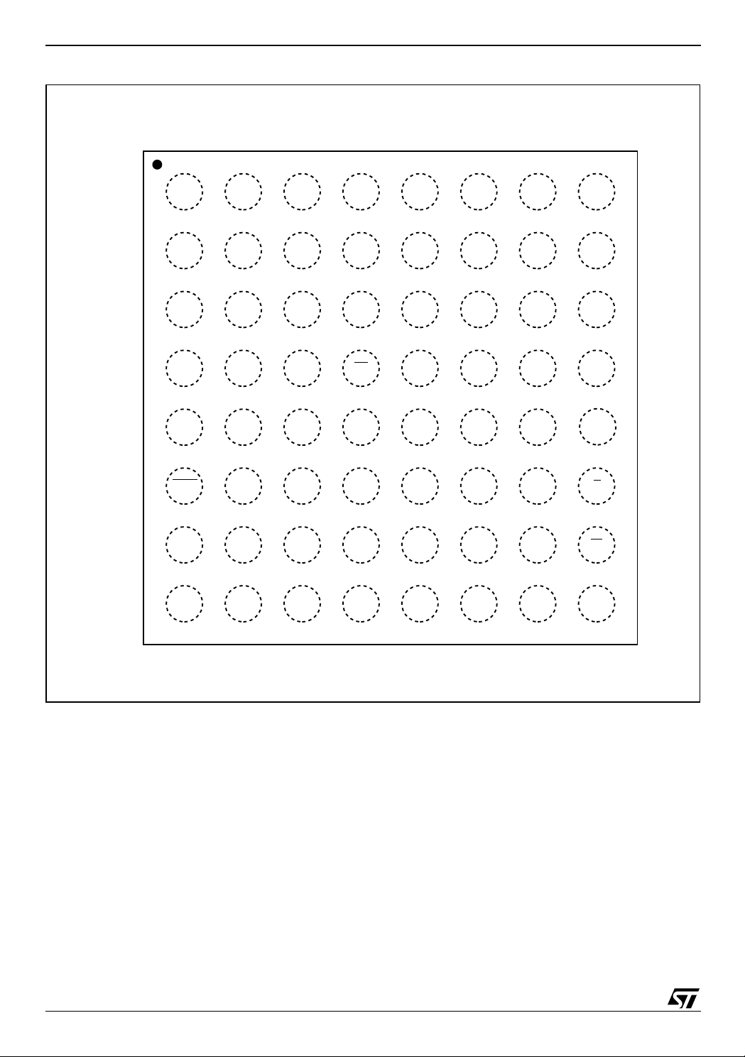
Figure 4. TBGA64 Connections (Top view through package)
87654321
A
B A19A2
C
D A16
E
F
G
H
A1
A4 A5
BYTE
NC
E2
A6 V
V
SS
A7A3
DQ0
A0
DU
A8
A10
A11
DQ10
DQ2
V
DD
V
PEN
E0A9
A12
RP
DDQ
SSQ
A13
A14
A15
DU DU
DQ5V
DQ13
V
DD
DU
DU
DU
DU DU
DQ6
V
SS
DQ15 STSDQ9DQ8 DQ1 DQ4DQ3
DQ14
DQ7
A18
A20
NC
E1
A21
A17
GDQ12DQ11
W
NC
8/51
AI06236b
Figure 5. Block Addresses
Byte (x8) Bus Width Word (x16) Bus Width
M58LW032D
3FFFFFh
3E0000h
3DFFFFh
3C0000h
03FFFFh
020000h
01FFFFh
000000h
Note: Also see A ppendix A, Table 23 for a full l i st i ng of the Block Addresses
1 Mbit or
128 KBytes
1 Mbit or
128 KBytes
Total of 32
1 Mbit Blocks
1 Mbit or
128 KBytes
1 Mbit or
128 KBytes
1FFFFFh
1F0000h
1EFFFFh
1E0000h
01FFFFh
010000h
00FFFFh
000000h
1 Mbit or
64 KWords
1 Mbit or
64 KWords
1 Mbit or
64 KWords
1 Mbit or
64 KWords
AI06238b
9/51

M58LW032D
SIGNAL DESCRIPTIONS
See Figure 2, Logic Diagram and Table 1, Signal
Names, for a brief overview of the signals connected to this device.
Address Input (A0). The A0 address input is
used to select the higher or lower Byte in X8 mode.
It is not used in X16 mode (where A1 is the Lowest
Significant bit).
Address Inputs (A1-A21). The Address Inputs are used to select the cells to access in the memory array during Bus Read operations either to read or to program data to. During Bus Write operations they control the commands sent to the Command Interface of the Program/Erase Controller.
The device must be enabled (refer to Table 2, Device Enable) when selecting the addresses. The
address inputs are latched on the rising edge of
Write Enable or on the first edge of Chip Enables
E0, E1 or E2 that disable the device, whichever
occurs first.
Data Inputs/Outputs (DQ0-DQ15). The Data Inputs/Outputs output the data stored at the selected address during a Bus Read operation, or are used to input the data during a program operation. During Bus Write operations they repres ent the commands sent to the Command Interface of the Program/Erase Controller. When used to input data or Write commands they are latched on t he rising edge of Write Enable or the first edge of Chip Enables E0, E1 or E2 that disable the device, whichever occurs first.
When the device is enabled and O utp ut Enab le is
low, V
bus outputs data from the memory array, the Electronic Signature, the Block Protection stat us, the
CFI Information or the contents of the Status Register. The data b us is high impedanc e when the
device is deselected, Output Enable is high, V
the Reset/Power-Down signal is low, V
the Program/Erase Controller is active the Ready/
Busy status is given on DQ7.
Chip Enables (E0, E1, E2). The Chip Enable inputs E0, E1 and E2 activate the memory control logic, input buffers, decoders and sense amplifiers. The device is selected at the first edge of Chip Enables E0, E1 or E2 that enable the device and deselected at the first edge of Chip E nables E0, E1 or E2 that disable the device. Refer to Table 2, Device Enable for more details.
When the Chip Enable inputs deselect the memory, power consumption is reduc ed to t he Standby
level, I
Output Enable (G
the outputs through the data output buffers during
a read operation. When Output Enable, G
the outputs are high impedance.
(refer to Table 2, Device Enable), the data
IL
. When
IL
.
DD1
). The Output Enable, G, gates
, is at V
IH,
or
IH
Write Enable (W
). The Write Enable input, W,
controls writing to the Command Interface, Input
Address and Data latches. Both addresses and
data can be latched on the rising edge of Write Enable.
Reset/Power-Down (RP
). The Reset/Power-
Down pin can be used to apply a Hardware Reset
to the me mory.
A Hardware Reset is achieved by holding Reset/
Power-Down Low, V
, for at least t
IL
Reset/Power-Down is Low, V
, the Status Regis-
IL
PLPH
. When
ter information is c leared and t he power consumption is reduced to power-down level. The device is
deselected and outputs are high impedance. If Reset/Power-Down goes low, V
,during a Block
IL
Erase, a Write to Buffe r and Program or a Block
Protect/Unprotect the operation is aborted and the
data may be corrupted. In this case the STS pin
stays low, V
until the completion of the Reset/Power-Down
BH,
, for a max imum t imi ng of t
IL
PLPH
+ t
PH-
pulse.
After Reset/Power-Down goes High, V
IH
, the
memory will be ready for Bus Read and Bus Write
operations after t
. Note that STS does not fall
PHQV
during a reset, see Ready/Busy Output section.
In an application, it is recommended to associate
Reset/Power-Down pin, RP
, with the reset sig nal
of the microprocessor. Otherwise, if a reset operation occurs while the memory is performing an
Erase or Program operation, the memory may output the Status Register information inst ead of being initialized to the default Asynchronous
Random Read.
Byte /Word Or ganizat ion Sel ect (BYT E
). The
Byte/Word Organization Select pin is used to
switch between the x8 and x16 bu s widths of the
memory. When Byte/Word Organizati on Select is
Low, V
High, V
, the memory is in x8 mode, when it is
IL
, the memory is in x16 mode.
IH
Status/(Ready/Busy) (STS). The STS signal is
an open drain output t hat can be used to id entify
the Program/Erase Controller status. It can be
configured in two modes:
■ Ready/Busy - the pin is Low, V
, during
OL
Program and Erase operations and high
impedance when the memory is ready for any
Read, Program or Erase operation.
■ Status - the pin gives a pulsing signal to indicate
the end of a Program or Block Erase operation.
After power-up or reset the STS pin i s configured
in Ready/Busy mode. T he pin can be co nfigured
for Status mode using the Configure STS command.
When the Program/Erase Controller is idle, or suspended, STS can float High through a pul l-up re-
10/51
M58LW032D
sistor. The use of an open-drain output allows the
STS pins from several memo ries to be c onnect ed
to a single pull-up resistor (a Low will indicate that
one, or more, of the memories is busy).
STS is not Low during a reset unless the reset was
applied when the Program/Erase controller was
active.
Program/Erase Enable (V
Erase Enable input, V
PEN,
). The Program/
PEN
is used to protect all
blocks, preventing Program and Erase operations
from affecting their data.
Program/Erase Enable must be kept High during
all Program/Erase Controller operations, otherwise the operations is not guaranteed to suc ceed
and data may become corrupt.
V
Supply Voltage. VDD provides the power
DD
supply to the internal core of the memory device.
It is the main power supply for all operations
(Read, Program and Erase).
Table 2. Device Enable
E2 E1 E0 Device
V
IL
V
IL
V
IL
V
IL
V
IH
V
IH
V
IH
V
IH
Note: For single device operations, E2 and E1 can be connected to VSS.
V
IL
V
IL
V
IH
V
IH
V
IL
V
IL
V
IH
V
IH
V
Supply Voltage. V
DDQ
provides the power
DDQ
supply to the I/O pins and enables all Outputs to
. V
be powered independently from V
tied to V
or can use a separate supply.
DD
DD
DDQ
can be
It is recommended to power-up and power-down
V
DD
and V
together to avoid any condition that
DDQ
would result in data corruption.
Ground. Ground, V
V
SS
is the reference for
SS,
the core power supply. It must be connected to the
system ground.
V
Ground. V
SSQ
the input/output circuitry driven by V
ground is the reference for
SSQ
DDQ
. V
SSQ
must be connected to VSS.
Note: Each device in a system should have
V
DD
and V
decoupled with a 0.1µF ceramic
DDQ
capacitor close to the pin (high frequency, inherently low inductance ca pacitors should b e
as close as possible to the package). See Figure 8, AC Measurement Load Circuit.
V
IL
V
IH
V
IL
V
IH
V
IL
V
IH
V
IL
V
IH
Enabled
Disabled
Disabled
Disabled
Enabled
Enabled
Enabled
Disabled
11/51
M58LW032D
BUS OPERATIONS
There are five standard bus operations that control
the memory. Each of these is described in this
section, see Tables 3, Bus Operations, for a summary.
On Power-up or after a Hardware Reset the memory defaults to Read Array mode (Page Read).
Typically glitches of less than 5ns on Chip Enable
or Write Enable are ignored by the memory and do
not affect bus operations.
Bus Read. Bus Read operations are used to output the contents of the Memory Array, the Electronic Signature, the Status Register, the Common
Flash Interface and the Block Protection Status.
A valid bus operation i nvolves set ting the des ired
address on the Address inputs, enabling the device (refer to Table 2, Device Enable), a pplying a
Low signal, V
Write Enable High, V
the previous command written to the memory (see
Command Interface section).
See Figure 9, Bus Read AC Waveforms, and Table 15, Bus Read AC Characteristics, for details of
when the output becomes valid.
Bus Write. Bus Write operations write Commands to the memory or latch addresses and input
data to be programmed.
A valid Bus Write operation begin s by setting the
desired address on the Address Inputs and enabling the device (refer to Chip Enable section).
, to Output Enable and keeping
IL
. The data read depends on
IH
The Address Inputs are latched by the Command
Interface on the rising edge of Write Enable or the
first edge of E0, E1 or E2 that disables the device
(refer to Table 2, Device Enable).
The Data Input/Outputs a re latched by the Command Interface on the rising edge of Write Enable
or the first edge of E0, E1 o r E2 that disables t he
device whichever occurs first. Output Enable must
remain High, V
, during the Bus Write operation.
IH
See Figures 11, and 12, Write AC Waveforms, and
Tables 17 and 18, Write and Chip Enable Controlled Write AC Characteristics, for details of the
timing requirements.
Output Disa bl e . The Data Inputs/Outputs are high impedance when the Output Enable is at V
IH
Power-Down. The memory is in Power-Down
mode when Reset/Power-Down, RP
, is Low. The
power consumption is reduced to the Power-Down
level, I
, and the out puts are high impedance,
DD2
independent of Chip Enable, Output Enable or
Write Enable.
Standby. Standby disables most of the internal
circuitry, allowing a substantial reduction of the
current consumption. The memory is in standby
when Chip Enable is at V
tion is reduced to the standby level I
. The power consump-
IH
DD1
and the
outputs are set to high impedance, independently
of the Output Enable or Write Enable inputs.
If Chip Enable switches to V
during a program or
IH
erase operation, the d ev ice en ters Standby mode
when finished.
.
Table 3. Bus Operations
or VIH.
E0, E1
or E2
V
IL
V
IL
V
IL
V
IH
Bus Operation
Bus Read
Bus Write
Output Disable
Power-Down X X X
Standby
Note: 1. DQ8-DQ15 are High Z in x8 mode.
2. X = Don’t Care V
12/51
IL
G
V
IL
V
IH
V
IH
XX
W RP
V
IH
V
IL
V
IH
V
IH
V
IH
V
IH
V
IL
V
IH
A1-A21 (x16)
A0-A21 (x8)
Address Data Output
Address Data Input
X High Z
X High Z
X High Z
DQ0-DQ15 (x16)
DQ0-DQ7 (x8)
(1)

READ MODES
Read operations in the M58LW032D are asynchronous. The device outputs the data corresponding to the address latched, that is the
memory array, Status Register, Common Flash Interface, Electronic Signature or Block Protection
Status depending on the command issued.
During read operations, if the bus is inactive for a
time equivalent to t
, the device autom at ically
AVQV
enters Auto Low Power mode. In this mode the internal supply current is reduced to the Auto Low
Power supply current, I
. The Data Inputs/Out-
DD5
puts will still output data if a Bus Read operation is
in progress.
Read operations can be performed in two different
ways, Random Read (where each Bus Read operation accesses a different Page) and Page Read.
M58LW032D
In Page Read mode a Page of data is internally
read and stored in a Page Buffer. Each memory
page is a 4 Words or 8 Bytes and has the same
A3-A21. In x8 mode only A0, A1 and A2 may
change, in x16 mode only A1 and A2 may change.
The first read operation within the Page has the
normal access time (t
within the same Page have much sho rter access
times (t
). If the Page changes then the nor-
AVQV1
mal, longer timings apply again.
See Figure 10, Page Read AC Waveforms and
Table 16, Page Read AC Characteristics for details on when the outputs become valid.
), subsequent reads
AVQV
13/51

M58LW032D
COMMAND INTERFACE
All Bus Write operations t o the me mory are in terpreted by the Command Interface. Commands
consist of one or more sequential Bus Write operations. The Commands are summarized in Table
4, Commands. Refer to Table 4 in conjunction with
the text descriptions below.
After power-up or a Reset operation the memory
enters Read mode.
Read Memory A rray Command. The Read Memory Array command is used to return the memory
to Read mode. One Bus Write cycle is required to
issue the Read Memory Array command and return the memory to Read mode. Once the command is issued the memory remains in Read
mode until another command is issued. From
Read mode Bus Read ope rations will access the
memory array. After power-up or a reset the memory defaults to Read Array mode (Page Read).
While the Program/Erase Controller is executing a
Program, Erase, Block Protec t, Blocks Unprotect
or Protection Register Program operation the
memory will not accept the Read Mem ory Array
command until the operation completes.
Read Electronic Si g nature Command . The Read
Electronic Signature command is used to read the
Manufacturer Code, the Device Code, t he Block
Protection Status and the Protection Register.
One Bus Write cycle is required to issue the Read
Electronic Signature command. Once the command is issued subsequ ent Bus Read operations
read the Manufacturer Code, the Device Code, the
Block Protection Status or the Protect ion Register
until another command is issued. Refer to Table 6,
Read Electronic Signature, Tables 7 an d 8, Word
and Byte-wide Read Protection Reg ister and F igure 6, Protection Register Memory Map for information on the addresses.
Read Query Command. The Read Query Command is used to read data from the Common Flash Interface (CFI) Memory Area. One Bus Write cycle is required to issue the Read Query Command. Once the command is issued subsequent Bus Read operations read from the Common Flash Interface Memory Area. See Appendix B, Tables 24, 25, 26, 27, 28 and 29 for details on the information contained in the Common Flash Interface (CFI) memory area.
Read Statu s Register Co mm an d . The Read Status Register command is us ed to read the Status
Register. One Bus Write cycle is required to issue
the Read Status Register command. Once the
command is issued subsequent Bus Read operations read the Status Register until another command is issued.
The Status Register information is present on the
output data bus (DQ1-DQ7) when the device is enabled and Output Enable is Low, V
.
IL
See the section on the Status Register and Table
10 for details on the definitions of the Status Register bits
Clear Status Register Command. The Clear Status Register command can be used to reset bits
SR1, SR3, SR4 and SR5 in the Status Register to
‘0’. One Bus Write is required to issue the Clear
Status Register command.
The bits in the Status Register are stic ky and do
not automatically return to ‘0’ when a new Write to
Buffer and Program, Erase, Block Protect, Block
Unprotect or Protection Register Program command is issued. If any error occurs then it is essential to clear any error bits in the Status Register by
issuing the Clear Status Register command before
attempting a new Program, Erase or Resume
command.
Block Erase Command. The Block Erase command can be used to e rase a block. I t sets all of
the bits in the block to ‘1’. All previous data in the
block is lost. If the block is protected then the
Erase operation will abort, the data in the block will
not be changed and the Status Register will output
the error.
Two Bus Write operations are required to issue the
command; the second Bus Write cycle latches the
block address and starts the Program/Erase Controller. Once the command is issued subsequent
Bus Read operations read the Status Register.
See the section on the Status Register for det ails
on the definitions of the Status Register bits.
During the Erase operation the memory will only
accept the Read Status Register command and
the Program/Erase Su spend command. All ot her
commands will be ignored. Typical Erase times
are given in Table 9.
See Appendix C, Figure 18, Block Erase Flowchart and Pseudo Code, for a suggested flowchart
on using the Block Erase command.
Word/Byte Program Command. The Word/
Byte Program command is used to program a single Word or Byte in the memory array. Two Bus
Write operations are required to issue the command; the first write cycle sets up the Word Program command, the second write cycle latches the
address and dat a to be programmed, and starts
the Program/Erase Controller.
If the block being program m ed i s prote cted an error will be set in the Status Register and the operation will abort without affecting the data in the
memory array. The block must be unprotected using the Blocks Unprotect command or by using the
14/51

M58LW032D
Blocks Temporary Unprotect feature of the Reset/
Power-Down pin, RP
.
Write to Buffer and Program Command. The Write to Buffer and Program comm and is used to program the memory array.
Up to 16 Words/32 Bytes can be load ed into the
Write Buffer and programmed into the memory.
Each Write Buffer has the same A5-A 21 add resses. In Byte-wide mode only A0-A4 may change in
Word-wide mode only A1-A4 may change, in .
Four successive steps are required to issue the
command.
1. One Bus Write o peration is required to set up
the Write to Buffer and Program Comm and. Issue the set up command with the selected
memory Block Address where the program operation should occur (any address in the block
where the values will be programmed can be
used). Any Bus Read operations will start to output the Status Register after the 1st cycle.
2. Use one Bus Write operation to write the same
block address along with the value N on the
Data Inputs/Output, where N+1 is the number of
Words/Bytes to be programmed.
3. Use N+1 Bus Write operations to load the address and data for each Word into the Write
Buffer. See the constraints on the address c ombinations listed below. The addresses must
have the same A5-A21.
4. Finally, use one Bus Write operation to issue the
final cycle to confirm the command and start the
Program operation.
Invalid address combinations or failing to follow
the correct sequence of Bus Write cycles will set
an error in the Status Register and abort the operation without affecting the data in the memory array. The Status Register should be cleared before
re-issuing the command.
If the block being program m ed i s prote cted an error will be set in the Status Register and the operation will abort without affecting the data in the
memory array. The block must be unprotected using the Blocks Unprotect command.
See Appendix C, Figure 16, Write to Buffer and
Program Flowchart and Pseudo Code, for a suggested flowchart on using the W rite to Buf fer and
Program command.
Program/Erase Suspend Command. The Program/Erase Suspend command is used to pause a
Word/Byte Program, Write to Buffer and Program
or Erase operation. The command will only be accepted during a Program or an Erase operation. It
can be issued at any tim e during an Erase operation but will only be accepted during a Word Program or Write to Buf fer and P rogram comman d if
the Program/Erase Controller is running.
One Bus Write cycle is required to i ssue the P rogram/Erase Suspend command and pause the
Program/Erase Controller. Once the command is
issued it is necessary to poll the Program/Erase
Controller Status bit (SR7) to find out when the
Program/Erase Controller has paused; no other
commands will be accepted until the Program/
Erase Controller has paused. After the Program/
Erase Controller has paused, the memory will continue to output the Status Register until another
command is issued.
During the polling period between issuing the Program/Erase Suspend command and the Program/
Erase Controller pausing it is possible for the operation to complete. Once the Program/Erase
Controller Status bit (SR7) indicates t hat the Program/Erase Controller is no longer active, the Program Suspend Status bit (SR2) or the Erase
Suspend Status bit (SR6) can be used to determine if the operation has completed or is suspended. For timing on the delay between issuing the
Program/Erase Suspend command and the Program/Erase Controller pausing see Table 9.
During Program/Erase Suspend the Read Memory Array, Read Status Register, Read Elect ronic
Signature, Read Query and Program/Erase Resume commands will be accepted by the Command Interface. Additionally, if the suspended
operation was Erase then the W rite to B uffer and
Program, and the Program Suspend commands
will also be ac cepted. W hen a program o peration
is completed inside a Block Erase Suspend the
Read Memory Array command m ust be issued to
reset the device in Read mode, then the Erase Resume command can be issued to complete the
whole sequence. Only the blocks not being erased
may be read or programmed correctly.
See Appendix C, Figure 17 , Program Suspend &
Resume Flowchart and Pseudo Code, and Figure
19, Erase Suspend & Resume Flowchart and
Pseudo Code, for suggested flowcharts on using
the Program/Erase Suspend command .
Program / Erase Resume Command. The Program/Erase Resume command can be used to restart the Program/Erase Controller after a
Program/Erase Suspend operat ion h as paused it.
One Bus Write cycle is required to i ssue the P rogram/Erase Resume command. Once the command is issued subsequ ent Bus Read operations
read the Status Register.
Block Protect Command. The Block Protect command is used to protec t a block and prevent Program or Erase operations from changing the data in it. Two Bus Write cycles are required to issue the Block Protect command; the second Bus Write cycle latches the block address and starts the Program/Erase Controller. Once the command is issued subsequent Bus Read operations read
15/51

M58LW032D
the Status Register. See the section on the Status
Register for details on the definitions of the Status
Register bits.
During the Block Protect operation the memory will
only accept the Read Sta tus Register command.
All other commands will be ignored. Typical Block
Protection times are given in Table 9.
The Block Protection bits are non-volatile, once
set they remain set through reset and powerdown/power-up. They ar e cleared by a Blocks Unprotect command.
See Appendix C, Figure 20, Block Protect Flowchart and Pseudo Code, for a suggested flowchart
on using the Block Protect command.
Blocks Unprotect Command. The Blocks Unprotect command is used to unprotect all of the blocks. Two Bus Write cycles are requir ed to issue the Blocks Unprotect command ; the second Bus Write cycle starts the Program/Erase Controller. Once the command is issued subsequent Bus Read operations read the Status Register. See the section on the Stat us Register for details on the definitions of the Status Register bits.
During the Block Unprotect operation the memory
will only accept the Read Status Register command. All other commands will be ignored. Typical
Block Protection times are given in Table 9.
See Appendix C, Figure 21, Block Unprotect Flowchart and Pseudo Code, for a suggested flowchart
on using the Block Unprotect command.
Protection Regist er Progr am Command. The
Protection Register Program c omm and is used to
Program the 64 bit user segment of the Protection
Register. Two write cycles are required to issue
the P rotection Registe r Program com mand.
■ The first bus cycle sets up the Protection
Register Program command.
■ The second latches the Address and the Data to
be written to the Protection Register and starts
the Program/Erase Controller.
Read operations output the Status Register content after the programming has started.
The user-programmable segment can be locked
by programming bi t 1 of t he Protection Register
Lock location to ‘0’ (see Table 7 and x for Wordwide and Byte-wide protection addressing). Bit 0
of the Protection Register Lock location locks the
factory programmed segment and is programmed
to ‘0’ in the factory. The locking of the Protection
Register is not reversible, once the lock bits are
programmed no further c hanges ca n be made t o
the values stored in the Protection Register, see
Figure 6, Protection Register Memory Map. Attempting to program a previously protected Protection Register will result in a Status Register
error.
The Protection Register Program cannot be suspended. See Appendix C, Figure 22, Protection
Register Program Flowchart and Pseudo Code,
for the flowchart for using the P rotection Regi ster
Program command.
Configure STS Command.
The Configure STS command is used to configure
the Status/(Ready/Busy) pin. After power-up or reset the STS pin is configured in Ready/Busy
mode. The pin can be configured in Status mode
using the Configure STS command (refer to Status/(Ready/Busy) section for more details.
Two write cycles are required to issue the Configure STS command.
■ The first bus cycle sets up the Configure STS
command.
■ The second specifies one of the four possible
configurations (refer to Table 5, Configuration
Codes):
– Ready/Busy mode
– Pulse on Erase complete mo de
– Pulse on Program complete mod e
– Pulse on Erase or Program complete mode
The device will not accept the Configure STS command while the Program/Erase controller is busy
or during Program/Erase Suspend. When STS pin
is pulsing it remains Low for a typical time of
250ns. Any invalid Configuration Code will set an
error in the Status Register.
16/51

Table 4. Commands
M58LW032D
Bus Operations
Command
Cycles
1st Cycle 2nd Cycle Subsequent Final
Op. Addr. Data Op. Addr. Data Op. Addr. Data Op. Addr. Data
Read Memory Array ≥ 2 Write X FFh Read RA RD
Read Electronic Signature ≥ 2 Write X 90h Read
IDA
(2)
IDD
(2)
Read Status Register 2 Write X 70h Read X SRD
Read Query ≥ 2 Write X 98h Read
QA
(3)
QD
(3)
Clear Status Register 1 Write X 50h
Block Erase 2 Write X 20h Write BA D0
Word/Byte Program 2 Write X
Write to Buffer and
Program
4 + N Write BA E8h Write BA N Write PA PD Write X D0h
40h
Write PA PD
10h
Program/Erase Suspend 1 Write X B0h
Program/Erase Resume 1 Write X D0h
Block Protect 2 Write X 60h Write BA 01h
Blocks Unprotect 2 Write X 60h Write X D0h
Protection Register
Program
2 Write X C0h Write PRA PRD
Configure STS command 2 Write X B8h Write X CC
Note: 1. X Don’t Care; RA Read Address, RD Read Data, IDA Identifier Address, IDD Identifier Data, SRD Status Register Data, PA Program
Address; PD Program Dat a, QA Quer y Address, QD Query Data, BA Any address in the Bloc k, PRA Prot ection register address,
PRD Prote ct i on Register Data, CC Configur at i on Code.
2. For Ident ifi er address es and data refer to Table 6, Read Electr onic Signa tu re.
3. For Query A ddress and Da ta refer to App endix B, CFI .
Table 5. Configuration Codes
Configuration
Code
00h 0 0 Ready/Busy
01h 0 1
02h 1 0
03h 1 1
Note: 1. DQ2-DQ7 are reserved
2. When STS pi n i s pulsing it remains Low for a typical time of 250ns.
DQ1 DQ2 Mode STS Pin Description
V
operations
Hi-Z when the
memory is ready
Pulse on Erase
complete
Pulse on
Program
complete
Pulse on Erase
Pulse Low then
High when
operation
completed
or Program
complete
during P/E
OL
The STS pin is Low during Program and
Erase operations and high impedance when
the memory is ready for any Read, Program
or Erase operation.
Supplies a system interrupt pulse at the end
of a Block Erase operation.
Supplies a system interrupt pulse at the end
of a Program operation.
(2)
Supplies a system interrupt pulse at the end
of a Block Erase or Program operation.
17/51

M58LW032D
Table 6. Read Electronic Signatur e
Code Bus Width
x8
Manufacturer Code
x16 0020h
x8
Device Code
x16 0016h
Address (A21-A1)
000000h
000001h
(3)
Data (DQ15-DQ0)
20h
16h
x8
Block Protection Status
SBA
(1)
+02h
x16
Protection Register x8, x16
Note: 1. SBA is the Start Base Addr ess of each blo ck , PRD is Protection Register Dat a.
2. Base Add r ess, refer to Fig ure 6 and Tabl es 7 and 8 for m ore infor m ation.
3. A0 is not used in Read Electronic Signature in either x8 or x16 mode. The data is always presented on the lower byte in x16 mode.
000080h
(2)
00h (Block Unprotected)
01h (Block Protected)
0000h (Block Unprotected)
0001h (Block Protected)
(1)
PRD
Figure 6. Prot ect i on Register Mem ory Map
WORD
ADDRESS
88h
User Programmable
85h
84h
81h
80h
Unique device number
Protection Register Lock 1 0
AI05501
Table 7. Word-Wide Read Protection Register
Word Use A8 A7 A6 A5 A4 A3 A2 A1
Lock Factory, User 10000000
0 Factory (Unique ID) 10000001
1 Factory (Unique ID) 10000010
2 Factory (Unique ID) 10000011
3 Factory (Unique ID) 10000100
4 User 10000101
5 User 10000110
6 User 10000111
7 User 10001000
18/51

M58LW032D
Table 8. Byte-Wide Read Protection Register
Word Use A8 A7 A6 A5 A4 A3 A2 A1
Lock Factory, User 10000000
Lock Factory, User 10000000
0 Factory (Unique ID) 10000001
1 Factory (Unique ID) 10000001
2 Factory (Unique ID) 10000010
3 Factory (Unique ID) 10000010
4 Factory (Unique ID) 10000011
5 Factory (Unique ID) 10000011
6 Factory (Unique ID) 10000100
7 Factory (Unique ID) 10000100
8 User 10000101
9 User 10000101
A User 10000110
B User 10000110
C User 10000111
D User 10000111
E User 10001000
F User 10001000
19/51

M58LW032D
Table 9. Program, Erase Times and Progra m Erase Endurance Cycles
Parameters
Min
Block (1Mb) Erase 1.2
Chip Program (Write to Buffer) 24
Chip Erase Time 37
Program Write Buffer
Word/Byte Program Time
(Word/Byte Program command)
Program Suspend Latency Time 1
Erase Suspend Latency Time 1
Block Protect Time 18
Blocks Unprotect Time 0.75
Program/Erase Cycles (per block) 100,000 cycles
Data Retention 20 years
Note: 1. T ypical values measured at room tem perature and nominal voltages.
2. Sampled, but not 100% tested.
3. Effective byte progr am m i ng time 6µs , effective word programming time 12 µs.
4. Maximum value measu red at worst case conditions for both t em perature and V
5. Maximum value measu red at worst case conditions for both t em perature and V
M58LW032D
(1,2)
Typ
Max
4.8
110
(3)
192
16
576
48
20
25
30
1.2
after 100,000 program/erase cycles.
DD
.
DD
72
(4)
(4)
(4)
(5)
(5)
(5)
(5)
(2)
(4)
(4)
Unit
µs
µs
µs
µs
µs
s
s
s
s
20/51

STATUS REGISTER
The Status Register provides information on the
current or previous Program, Erase, Block Protect
or Blocks Unprotect operation. The various bits in
the Status Register convey information and errors
on the operation. They are output on DQ7-DQ0.
To read the Status Register the Read Status Register command can be issued. The Status Register
is automatically read after Program, Erase, Block
Protect, Blocks Unprotect and Program/Erase Resume commands. The Status Register can be
read from any address.
The contents of the Status Register can be updated during an Erase or Program operation by toggling the Output Enable pin or by dis-activating
and then reactivating t he device (refer to Table 2,
Device Enable).
Status Register bits SR5, S R4, SR 3 and SR1 are
associated with various error conditions and can
only be reset with the Clear Status Register command. The Status Register bits are summarized in
Table 10, Status Register Bits. Refer to Table 10
in conjunction with the following text descriptions.
Program/Erase Controller Status (SR7). The Progra m/Erase Controller Status bit indicates whether
the Program/Erase Controller is active or inactive.
When the Program/Erase Controller Status bit is
Low, V
, the Program/Erase Controller is active
OL
and all other Status Register bits are High Impedance; when the bit is High, V
, the Program/
OH
Erase Controller is inactive.
The Program/Erase Controller Status is Low im-
mediately after a Program/Erase Suspend command is issued until the Program/Erase Controller
pauses. After the Program/Erase Controller pauses the bit is High.
During Program, Erase, Block Protect and Blocks
Unprotect operations the Program/Erase Controller Status bit can be polled to find the end of the
operation. The other bits in the Status Register
should not be tested until the Program/Erase Controller completes the operation and the bit is High.
After the Program/Erase Cont roller completes its
operation the Erase S tatus, Program Status and
Block Protection Status bits should be tested for
errors.
Erase Suspend Status (SR6). The Erase Suspend Status bit indicates that an Erase o peration
has been suspended and is waiting to be resumed. The Erase Suspend Status should only be
considered valid when the Program/Erase Controller Status bit is High (Program/Erase Controller
inactive); after a Program/Erase Suspend command is issued the memory may still complete the
operation rather than entering the Suspend mode.
When the Erase Suspend Statu s bit is Low, V
OL
the Program/Erase Controller is active or has com-
M58LW032D
pleted its operation; when the bit is High, V
Program/Erase Suspend com mand has been issued and the memory is waiting for a Program/
Erase Resume command.
When a Program/Erase Re sume command is issued the Erase Suspend Status bit returns Low.
Erase Status (SR5). The Erase Status bit can be
used to identify if the memory has failed to verify
that the block has erased correctly or that all
blocks have been unprotected successfully. The
Erase Status bit should be read once the Program/
Erase Controller Status bit is High (Program/Erase
Controller inactive).
When the Erase St atu s bit i s Low, V
ory has successfully verified that the block has
erased correctly or all blocks have been unprotected successfully. When the Erase Status bit is
High, V
, the erase operation has failed. De-
OH
pending on the cause of the failure othe r Status
Register bits may also be set to High, V
■ If only the Erase Status bit (SR5) is set High,
V
then the Program/Erase Controller has
OH,
applied the maximum number of pulses to the
block and still failed to verify that the block has
erased correctly or that all the blocks have been
unprotected successfully.
■ If the failure is due to an erase or blocks
unprotect with V
low, VOL, then V
PEN
bit (SR3) is also set High, V
■ If the failure is due to an erase on a protected
block then Block Protection Status bit (SR1) is
also set High, V
■ If the failure is due to a program or erase
OH
.
incorrect command sequence then Program
Status bit (SR4) is also set High, V
Once set High, the Erase Status bit can only be reset Low by a Clear Status Register command or a
hardware reset. If set High it should be reset before a new Program or Erase command is issued,
otherwise the new command will appear to fail.
Program Status (SR4). The Program Status bit
is used to identify a Program or Block Pr otect failure. The Program S tatus bit shoul d be read once
the Program/Erase Controller Status bit is High
(Program/Erase Controller inactive).
When the Program Status bit is Low, V
memory has successfully verified that the Write
Buffer has programmed correc tly or the block is
protected. When the Program Status bit is High,
V
, the program or block protect operation has
OH
failed. Depending on the cause of the failure other
Status Register bits may also be set to High, V
■ If only the Program Status bit (SR4) is set High,
then the Program/Erase Controller has
V
,
OH,
applied the maximum number of pulses to the
OH
OL
.
OH
, the mem-
.
OH
Status
PEN
.
OH
OL
, a
, the
OH
.
21/51

M58LW032D
byte and still failed to verify that the Write Buffer
has programmed correctly or that the Block is
protected.
■ If the failure is due to a program or block protect
with V
is also set High, V
■ If the failure is due to a program on a protected
low, VOL, then V
PEN
OH
Status bit (SR3)
PEN
.
block then Block Protection Status bit (SR1) is
also set High, V
■ If the failure is due to a program or erase
OH
.
incorrect command sequence then Erase
Status bit (SR5) is also set High, V
OH
.
Once set High, the Program Status bit can only be
reset Low by a Clear Status Register command or
a hardware reset. If set High it should be reset before a new Program or Erase command is issued,
otherwise the new command will appear to fail.
Status (SR3). T he V
V
PEN
Status bit can be
PEN
used to identify if a Program, Erase, Block Protection or Block Unprotection operation has been a ttempted when V
When the V
PEN
is Low, VIL.
PEN
Status bit is Low, VOL, no Program, Erase, Block Protection or Block Unprotection operations have been attempted with V
PEN
Low, VIL, since the last Clear S tatus Register command, or hardware reset. When the V
bit is High, V
, a Program, Erase, Block Protec-
OH
PEN
Status
tion or Block Unprotection operation has been a ttempted with V
Once set High, the V
Low, VIL.
PEN
Status bit can only be re-
PEN
set by a Clear Status Register command or a hardware reset. If set High it should be reset befo re a
new Program, Erase, Block Protection or Block
Unprotection command is issued, otherwise the
new command will appear to fail.
Program Suspend Status (SR2). The Program
Suspend Status bit indicates that a Program oper-
ation has been suspended and is waiting to be resumed. The Program Suspend Status should only
be considered valid when the Program/Erase
Controller Status bit is High (Program/Erase Controller inactive); after a Program/Erase Suspend
command is issued the memory may still complete
the operation rather than entering the Suspend
mode.
When the Program Suspend Status bit is Low,
, the Program/Erase Controller is active or has
V
OL
completed its operation; when the bit is High, V
OH
a Program/Erase Suspend command has been issued and the memory is waiting for a Program/
Erase Resume command.
When a Program/Erase Re sume command is issued the Program Suspend Status bit returns Low.
Block Protection Status (SR1). The Block Protection Status bit can be used to identify if a Program or Erase operation has tried to modify the
contents of a protected block.
When the Block Protection Status bit is Low, V
OL
no Program or Erase operations have been attempted to protected blocks since the last Clear
Status Register command or hardware reset;
when the Block Protection Status bit is High, V
OH
a Program (Program St atus bit SR4 set High) or
Erase (Erase Status bit SR5 set High) operat ion
has been attempted on a protected block.
Once set High, the Block Protection Status bit can
only be reset Low by a Clear Status Register command or a hardware reset. If set High it should be
reset before a new Program or Erase command is
issued, otherwise the new command will appear to
fail.
Reserved (SR0). Bit SR0 of the Status Regi ster
is reserved. Its value should be masked.
,
,
,
22/51

M58LW032D
Table 10. Status Register Bits
OPERATION SR 7 SR6 SR5 SR4 SR3 SR2 SR1
Program/Erase Controller active 0 Hi-Z N/A
Write Buffer not ready 0 Hi-Z N/A
Write Buffer ready 1 0 0 0 0 0 0 80h
Write Buffer ready in Erase Suspend 1 1 0 0 0 0 0 C0h
Program suspended 1 0 0 0 0 1 0 84h
Program suspended in Erase Suspend 1 1 0 0 0 1 0 C4h
Program/Block Protect completed
successfully
Program completed successfully in Erase
Suspend
Program/Block protect failure due to incorrect
command sequence
Program failure due to incorrect command
sequence in Erase Suspend
Program/Block Protect failure due to
error
V
PEN
100000080h
1100000C0h
1011000B0h
1111000F0h
100110098h
Result
(Hex)
V
Program failure due to
Suspend
Program failure due to Block Protection 1 0 0 1 0 0 1 92h
Program failure due to Block Protection in
Erase Suspend
Program/Block Protect failure due to cell
failure
Program failure due to cell failure in Erase
Suspend
Erase Suspended 1 1 0 0 0 0 0 C0h
Erase/Blocks Unprotect completed
successfully
Erase/Blocks Unprotect failure due to
incorrect command sequence
Erase/Blocks Unprotect failure due to
error
Erase failure due to Block Protection 1 0 1 0 0 0 1 A2h
Erase/Blocks Unprotect failure due to failed
cells in Block
Configure STS error due to invalid
configuration code
error in Erase
PEN
V
PEN
1101100D8h
1101001D2h
100100090h
1101000D0h
100000080h
1011000B0h
1010100A8h
1010000A0h
1011000B0h
23/51

M58LW032D
MAXIMUM RATI N G
Stressing the device above the ratings listed in Table 11, Absolute Maximum Ratings, may cause
permanent damage to the device. These are
stress ratings only and operation of the dev ice at
these or any other conditions above those indicated in the Operating sections of this specification is
Table 11. Absolute Maximum Ratings
Symbol Parameter
T
BIAS
T
STG
V
IO
, V
V
DD
DDQ
I
OSC
Note: 1. M aximum one output shor t- ci rcuited at a tim e and for no lo nger than 1 sec ond.
Temperature Under Bias –40 125 °C
Storage Temperature –55 150 °C
Input or Output Voltage –0.6
Supply Voltage –0.6 5.0 V
Output Short-circuit Current
not implied. Exposure to Absol ute Maxim um Ra ting conditions for extended periods may affect device reliability. Refer also to the
STMicroelectronics SURE Program and other relevant quality documents.
Value
Min Max
V
DDQ
100
+0.6
(1)
Unit
V
mA
24/51

DC AND AC PARAMETERS
This section summarizes the operat ing and measurement conditions, and the DC and AC characteristics of the device. The parameters in t he DC
and AC characteristics Tables that follow, are derived from tests performed under the Measure-
ment Conditions summarized in Table 12,
Operating and AC Measurem ent Conditions. Designers should check that the operating conditions
in their circuit match the measurement conditions
when relying on the quoted parameters.
Table 12. Operating and AC Measurement Conditions
Parameter
Supply Voltage (V
Input/Output Supply Voltage (V
Ambient Temperature (T
Load Capacitance (C
Input Pulses Voltages
Input and Output Timing Ref. Voltages
DD
)
)
DDQ
)
A
)
L
Grade 1 0 70 °C
Grade 6 –40 85 °C
M58LW032D
M58LW032D
Min Max
2.7 3.6 V
2.7
3.6
30 pF
0 to V
DDQ
0.5 V
DDQ
Units
V
V
V
Figure 7. AC Me asureme nt In put Ou t put Waveform
V
DDQ
0.5 V
0V
DDQ
AI00610
Figure 8. AC Me asureme nt Load Circui t
1.3V
V
DDQ
V
DD
DEVICE
UNDER
TEST
0.1µF
0.1µF
CL includes JIG capacitance
Table 13. Capacitance
Symbol Parameter Test Condition Typ Max Unit
C
IN
C
OUT
Note: 1. TA = 25°C, f = 1 MHz
2. Sampled only, not 100% tested.
Input Capacitance
Output Capacitance
V
V
OUT
IN
= 0V
= 0V
68pF
812pF
1N914
3.3kΩ
CL
DQ
AI03459
S
25/51

M58LW032D
Table 14. DC Characteristics
Symbol Parameter Test Condition Min Max Unit
I
Input Leakage Curren t
LI
I
I
I
DDO
I
DD1
I
DD5
I
DD2
I
DD3
I
DD4
V
V
V
V
V
V
PENH
Output Leakage Current
LO
Supply Current (Random Read)
DD
Supply Current (Page Read)
Supply Current (Standby)
Supply Current (Auto Low-Power)
Supply Current (Reset/Power-Down)
Supply Current (Program or Erase,
Block Protect, Block Unprotect)
Supply Current
(Erase/Program Suspend)
Input Low Voltage –0 .5 0.8 V
IL
Input High Voltage 2
IH
Output Low Voltage
OL
Output High Voltage
OH
VDD Supply Voltage (Erase and
LKO
Program lockout)
V
Supply Voltage (block erase,
PEN
program and block protect)
0V ≤ V
0V
E
E
E
E
≤ V
IN
DDQ
≤ V
≤ V
OUT
DDQ
= VIL, f=5MHz
= VIL, f=33MHz
= VIH, RP = V
= VIL, RP = V
RP
= V
IL
IH
IH
Program or Erase operation in
progress
= V
E
IH
I
= 100µA
OL
I
= –100µA V
OH
±1 µA
±5 µA
20 mA
29 mA
40 µA
40 µA
40 µA
30 mA
40 µA
V
DDQ
+ 0.5
V
0.2 V
DDQ
–0.2
V
2V
2.7 3.6 V
26/51

Figure 9. Bus Read AC Waveforms
A0-A21
tELQV
E2, E1, E0
(1)
M58LW032D
tAVAV
VALID
tAXQXtELQX
tGLQV
tGLQX
G
tELBL
(2)
BYTE
tBLQV
tBLQZ
tAVQV
DQ0-DQ15
Note: 1. VIH = Devi ce Dis ab led (firs t edg e o f E0 , E 1 or E 2), VIL = Device E na bled (firs t ed ge of E 0, E1 or E2). Ref er t o Ta ble 2 for mor e
details.
can be Low or High.
2. BYTE
OUTPUT
tEHQZ
tEHQX
tGHQZ
tGHQX
AI06239b
Table 15. Bus Read AC Characteristics.
Symbol Parameter Test Condition
t
AVAV
t
AVQV
t
AXQX
t
BLQV
t
BLQZ
t
EHQX
t
EHQZ
t
ELBL
t
ELQX
t
ELQV
t
GHQX
t
GHQZ
t
GLQX
t
GLQV
Address Valid to Address Valid
Address Valid to Output Valid
Address Transition to Output Transition
Byte Low (or High) to Output Valid
Byte Low (or High) to Output Hi-Z
Chip Enable High to Output Transition
Chip Enable High to Output Hi-Z
Chip Enable Low to Byte Low (or High)
Chip Enable Low to Output Transition
Chip Enable Low to Output Valid
Output Enable High to Output Transition
Output Enable High to Output Hi-Z
Output Enable Low to Output Transition
Output Enable Low to Output Valid
E
= VIL, G = V
E
= VIL, G = V
E
= VIL, G = V
E
= VIL, G = V
E
= VIL, G = V
G
= V
G
= V
G
= V
G
= V
G
= V
E
= V
E
= V
E
= V
E
= V
IL
IL
IL
IL
IL
IL
IL
IL
IL
IL
IL
IL
IL
IL
Min 90 110 ns
Max 90 110 ns
Min 0 0 ns
Max 1 1 µs
Max 1 1 µs
Min 0 0 ns
Max 25 25 ns
Max 10 10 ns
Min 0 0 ns
Max 90 110 ns
Min 0 0 ns
Max 15 15 ns
Min 0 0 ns
Max 25 25 ns
M58LW032D
Unit
90 110
27/51

M58LW032D
Figure 10. Page Read AC Waveforms
A1-A2
A3-A21
tAVQV
E2, E1, E0
DQ0-DQ15
Note: 1. VIH = Devi ce Dis ab led (firs t edg e o f E0 , E 1 or E 2), VIL = Device E na bled (firs t ed ge of E 0, E1 or E2). Ref er t o Ta ble 2 for mor e
details.
(1)
G
VALID VALID
VALID
tELQV
tGLQV
tGLQX
OUTPUT OUTPUT
tAVQV1
tAXQX1
tAXQXtELQX
tEHQZ
tEHQX
tGHQZ
tGHQX
AI06240
Table 16. Page Read AC Characteristics
Symbol Parameter Test Condition
t
AXQX1
t
AVQV1
Note: For other timings see Table 15, Bus Read AC Characteristics.
Address Transition to Output Transition
Address Valid to Output Valid
E
= VIL, G = V
E
= VIL, G = V
Min 6 ns
IL
Max 25 ns
IL
M58LW032D
Unit
90 - 110
28/51

Figure 11. Write AC Waveform, Write Enable Controlled
M58LW032D
A0-A21
V
(1)
tELWL
G
tGHWL
W
STS
PEN
E2, E1, E0
DQ0-DQ15
(Ready/Busy mode)
Note: 1. VIH = Devi ce Dis ab led (firs t edg e o f E0 , E 1 or E 2), VIL = Device E na bled (firs t ed ge of E 0, E1 or E2). Ref er t o Ta ble 2 for mor e
details.
tAVWH
tVPHWH
VALID
tWLWH
tDVWH
tWHEH
INPUT
tWHAX
tWHDX
tWHBL
tWHWL
tWHGL
AI06241
Table 17. Write AC Characteristics, Write Enable Controlled
Symbol Parameter Test Condition
t
AVWH
t
DVWH
t
ELWL
t
VPHWH
t
WHAX
t
WHBL
t
WHDX
t
WHEH
t
GHWL
t
WHGL
t
WHWL
t
WLWH
Address Valid to Write Enable High
Data Input Valid to Write Enable High
Chip Enable Low to Write Enable Low Min 0 ns
Program/Erase Enable High to Write Enable High Min 0 ns
Write Enable High to Address Transition
Write Enable High to Status/(Ready/Busy) low Max 500 ns
Write Enable High to Input Transition
Write Enable High to Chip Enable High Min 0 ns
Output Enable High to Write Enable Low Min 20 ns
Write Enable High to Output Enable Low Min 35 ns
Write Enable High to Write Enable Low Min 30 ns
Write Enable Low to Write Enable High
E
E
E
E
E
= V
= V
= V
= V
= V
IL
IL
IL
IL
IL
Min 50 ns
Min 50 ns
Min 0 ns
Min 0 ns
Min 70 ns
M58LW032D
Unit
90 - 110
29/51

M58LW032D
Figure 12. Write AC Waveforms, Chip Enable Controlled
A0-A21
W
tWLEL
G
STS
V
PEN
details.
(1)
E2, E1, E0
DQ0-DQ15
(Ready/Busy mode)
Note: 1. VIH = Devi ce Dis ab led (firs t edg e o f E0 , E 1 or E 2), VIL = Device E na bled (firs t ed ge of E 0, E1 or E2). Ref er t o Ta ble 2 for mor e
tAVEH
VALID
tELEH
tDVEH
tVPHEH
INPUT
tEHAX
tEHWH
tEHDX
tEHBL
tEHEL
tEHGLtGHEL
AI06242
Table 18. Write AC Characteristics, Chip Enable Controlled.
Symbol Parameter Test Condition
t
AVEH
t
DVEH
t
WLEL
t
VPHEH
t
EHAX
t
EHBL
t
EHDX
t
EHWH
t
GHEL
t
EHGL
t
EHEL
t
ELEH
Address Valid to Chip Enable High
Data Input Valid to Chip Enable High
Write Enable Low to Chip Enable Low Min 0 ns
Program/Erase Enable High to Chip Enable High Min 0 ns
Chip Enable High to Address Transition
Chip Enable High to Status/(Ready/Busy) low Max 500 ns
Chip Enable High to Input Transition
Chip Enable High to Write Enable High Min 0 ns
Output Enable High to Chip Enable Low Min 20 ns
Chip Enable High to Output Enable Low Min 35 ns
Chip Enable High to Chip Enable Low Min 30 ns
Chip Enable Low to Chip Enable High
W
W
W
W
W
= V
= V
= V
= V
= V
IL
IL
IL
IL
IL
Min 50 ns
Min 50 ns
Min 0 ns
Min 0 ns
Min 70 ns
M58LW032D
Unit
90 - 110
30/51

Figure 13. Reset, Power-Down and Power-Up AC Waveform
W
E2, E1, E0
(Ready/Busy mode)
(1)
DQ0-DQ15
STS
VDD, V
DDQ
, G
tPHQV
RP
tVDHPH tPLPH
Power-Up
and Reset
M58LW032D
tPHWL
tPLBH
Reset during
Program or Erase
AI06217b
Note: 1. VIH = Devi ce Dis ab led (firs t edg e o f E0 , E 1 or E 2), VIL = Device E na bled (firs t ed ge of E 0, E1 or E2). Ref er t o Ta ble 2 for mor e
details.
Table 19. Reset, Power-Down and Power-Up AC Character istics
Symbol Parameter
t
PHQV
t
PHWL
t
PLPH
t
PLBH
t
VDHPH
Reset/Power-Down High to Data Valid Max 130 150 ns
Reset/Power-Down High to Write Enable Low Max 1 1
Reset/Power-Down Low to Reset/Power-Down High Min 100 100 ns
Reset/Power-Down Low to Status/(Ready/Busy) High Max 30 30 µs
Supply Voltages High to Reset/Power-Down High Min 0 0 µs
M58LW032D
Unit
90 110
µs
31/51

M58LW032D
PACKAGE MECHANICAL
Figure 14. TSOP56 - 56 lead Plastic Thin Small Outline, 14 x 20 mm, Package Outline
A2
1
N
e
E
B
N/2
D1
D
DIE
A
CP
C
TSOP-a
Note: Drawing is not to scale.
LA1 α
Table 20. TSOP56 - 56 lead Plastic Thin Small Outline, 14 x 20 mm, Package M echa nical Data
Symbol
Typ Min Max Typ Min Max
A 1.20 0.0472
mm inches
A1 0.05 0.1 5 0.0020 0.0059
A2 0.95 1.0 5 0.0374 0.0413
B 0.17 0.27 0.0067 0.0106
C 0.10 0.21 0.0039 0.0083
D 19.80 20.20 0.7795 0 .7953
D1 18.30 18.50 0.7205 0 .7283
E 13.90 14.1 0 0.5472 0.5551
e 0.50 – – 0.0197 – –
L 0.50 0.70 0.0197 0.0276
α 0° 5° 0° 5°
N56 56
CP 0.10 0.0039
32/51

Figure 15. TBGA64 - 10x13mm, 8 x 8 ball array 1mm pitch, Package Outlin e
D
FD
FE
D1
SD
M58LW032D
SE
ddd
A2
A1
BGA-Z23
Note: Drawing is not to scale.
E1E
BALL "A1"
A
eb
Table 21. TBGA64 - 10x13mm, 8 x 8 ball array, 1 mm pitch, Package Mechanical Data
Symbol
Typ Min Max Typ Min Max
A 1.200 0.0472
A1 0.300 0.200 0.350 0.0118 0.0079 0.0138
A2 0.850 0.0335
b 0.400 0.500 0.0157 0 .0197
D 1 0.000 9.900 10.100 0.3937 0.3898 0.3976
D1 7.000 – – 0.2756 – –
ddd 0.100 0.0039
millimeters inches
e 1.000 – – 0.0394 – –
E 13.000 12.900 13.1 00 0.5118 0.5079 0.5157
E1 7.000 – – 0.2756 – –
FD 1 .500 – – 0.0591 – –
FE 3.000 – – 0.1181 – –
SD 0.500 – – 0.0197 – –
SE 0 .500 – – 0.0197 – –
33/51

M58LW032D
PART NUMBERING
Table 22. Ordering Information Scheme
Example: M58L W032D 110 N 1 T
Device Type
M58
Architecture
L = Page Mode
Operating Voltage
W = V
Device Function
032D = 32 Mbit (x8, x16), Uniform Block
Speed
110 = 110ns
90 = 90ns
DD
= V
= 2.7V to 3.6V
DDQ
Package
N = TSOP56: 14 x 20 mm
ZA = TBGA64: 10 x 13 mm, 1mm pitch
Temperature Rang e
1 = 0 to 70 °C
6 = –40 to 85 °C
Option
Blank = Standard Packing
T = Tape & Reel Packing
E = Lead-free Package, Standard Packing
F = Lead-free Package, Tape & Reel Packing
Note: Devices are shipped from the factory with the memory content bits erased to ’1’.
For a list of available options (Speed, Package, etc.) or for further information on any aspect of this device,
please contact the ST Sales Office nearest to you.
34/51

APPENDIX A. BLOCK ADDRESS TABLE
Table 23. Block Addresses
Block
Number
32 3E0000h-3 FFFFFh 1F0000h-1FFF FFh
31 3C0000h-3DFFFFh 1E0000h-1EFF FFh
30 3A0000h-3BFFFFh 1D00 00h- 1DFF FFh
29 380000h-3 9FFFFh 1C0000h-1CFFFFh
28 360000h-3 7FFFFh 1B0000h- 1BFF FFh
27 340000h-3 5FFFFh 1A0000h- 1AFF FFh
26 320000h-3 3FFFFh 190000h- 19FF FFh
25 300000h-3 1FFFFh 180000h- 18FF FFh
24 2E0000h-2 FFFFFh 1700 00h- 17FF FFh
23 2C0000h-2DFFFFh 160000h-16FFFFh
22 2A0000h-2BFFFFh 150000h- 15FF FFh
21 280000h-2 9FFFFh 140000h- 14FF FFh
20 260000h-2 7FFFFh 130000h- 13FF FFh
19 240000h-2 5FFFFh 120000h- 12FF FFh
Address Range
(x8 Bus Width)
Address Range
(x16 Bus Width)
M58LW032D
18 220000h-2 3FFFFh 110000h-11FFFFh
17 200000h-2 1FFFFh 100000h- 10FF FFh
16 1E0000h-1 FFFFFh 0F0000h-0FFF FFh
15 1C0000h-1DFFFFh 0E0000h-0EFF FFh
14 1A0000h-1BFFFFh 0D00 00h- 0DFF FFh
13 180000h-1 9FFFFh 0C0000h-0CFFFFh
12 160000h-1 7FFFFh 0B0000h- 0BFF FFh
11 1400 00h-1 5FFFFh 0A0000h- 0AFF FFh
10 120000h-1 3FFFFh 090000h- 09FF FFh
9 100000h-11FFFFh 080000h- 08FF FFh
8 0E0000h-0FFFF Fh 0700 00h- 07FF FFh
7 0C00 00h-0DFFF Fh 060000h-06FFFFh
6 0A0000h-0BFFFFh 050000h- 05FF FFh
5 080000h-09FFFFh 040000h- 04FF FFh
4 060000h-07FFFFh 030000h- 03FF FFh
3 040000h-05FFFFh 020000h- 02FF FFh
2 020000h-03FFFFh 010000h- 01FF FFh
1 000000h-01FFFFh 000000h- 00FF FFh
35/51

M58LW032D
APPENDIX B. COMMON FLASH INTERFACE - CFI
The Common Flash Interface is a JEDEC approved, standardized data structure that can be
read from the Flash memory device. It allows a
system software to query the device to det ermine
various electrical and t iming parameters, density
information and functions supported by the memory. The system can interface easily with the de-
Table 24. Query Structure Overview
Address
x16
x8
(4)
0000h 00h Manufacturer Code
0001h 02h Device Code
0010h 20h CFI Query Identification String Command set ID and algorithm data offset
001Bh 36h System Interface Information Device timing and voltage information
0027h 4Eh Device Geometry Definition Flash memory layout
Sub-section Name Description
vice, enabling the software to upgrade itself when
necessary.
When the CFI Query C ommand (RCFI) is issued
the device enters CFI Query mode and the data
structure is read from the memory. Tables 24 , 25,
26, 27, 28 and 29 show the addresses used to retrieve the data.
P(h)
A(h)
(1)
(2)
Primary Algorithm-specific Extended
Query Table
Alternate Algorithm-specific Extended
Query Table
Additional information specific to the Primary
Algorithm (optional)
Additional information specific to the Alternate
Algorithm (optional)
(SBA+02)h Block Status Register Block-related Information
Note: 1. Of fs et 15h defines P which points to the Pri m ary Algorith m Extended Query Addres s T able.
2. Offset 19h def i nes A which points to the Alt ernate Algo ri thm Extended Query Add ress Table .
3. SBA is the St art Base Address for each bl ock.
4. In x8 mode, A0 must be set to V
, otherwise 00h will be output.
IL
Table 25. CFI - Query Address and Data Output
Address
x16
0010h 20h 51h "Q"
0011h 22h 52h "R"
0012h 24h 59h "Y"
0013h 26h 01h
0014h 28h 00h
0015h 2Ah 31h
0016h 2Ch 00h
Data Description
x8
(3)
51h; "Q"
Query ASCII String 52h; "R"
Primary Vendor:
Command Set and Control Interface ID Code
Primary algorithm extended Query Address Table: P(h)
59h; "Y"
0017h 2Eh 00h
0018h 30h 00h
Alternate Vendor:
Command Set and Control Interface ID Code
0019h 32h 00h
(2)
001Ah
Note: 1. Query Data are always pr esented on DQ7-DQ0. DQ15-DQ8 are set to '0'.
2. Offset 19h defines A whic h poi nts to the Alt ernate Algorithm Extended Query Address Table.
3. In x8 mode, A0 must be set to V
34h 00h
, otherwise 00h will be output.
IL
Alternate Algorithm Extended Query address Table
36/51

Table 26. CFI - Device Voltage and Timing Specification
Address
x16
001Bh 36h
001Ch 38h
001Dh 3Ah
001Eh 3Ch
001Fh 3Eh
0020h 40h 08h
0021h 42h 0Ah
0022h 44h
0023h 46h
0024h 48h 04h
0025h 4Ah 04h
0026h 4Ch
Note: 1. Bit s are coded in B i nary Code Dec i m al , bit7 to bit4 are scaled in Vol t s and bit3 to bit 0 i n m V.
2. Bit7 to bit4 are coded in Hexadecim al and scaled in Volt s while bit3 to bit0 are in Binary Code Dec i m al and scaled i n 100mV.
3. Not supp ort ed.
4. In x8 mode, A0 must be set to V
Data Description
(1)
27h
36h
(2)
00h
00h
04h
00h
04h 2
(3)
00h
, otherwise 00h will be output.
IL
VDD Min, 2.7V
(1)
VDD max, 3.6V
VPP min – Not Available
(2)
VPP max – Not Available
2n µs typical time-out for Word, DWord prog – Not Available
n
2
µs, typical time-out for max buffer write
n
2
ms, typical time-out for Erase Block
(3)
2n ms, typical time-out for chip erase – Not Available
n
x typical for Word Dword time-out max – Not Available
n
2
x typical for buffer write time-out max
n
2
x typical for individual block erase time-out maximum
2n x typical for chip erase max time-out – Not Available
x8
(4)
M58LW032D
Table 27. Device Geometry Definition
Address
x16
0027h 4Eh 16h
0028h 50h 02 h Device Interface
0029h 52h 00h Organization Sync./Async.
002Ah 54h 05h
002Bh 56h 00h
002Ch 58h 01h Bit7-0 = number of Erase Block Regions in device
002Dh 5Ah 1Fh
002Eh 5Ch 00h
002Fh 5Eh 00h
0030h 60h 02h
Note: 1. In x8 mode, A0 must be set to VIL, otherwise 00h will be output.
Data Description
n
n where 2
is number of bytes memory Size
x8
(1)
Maximum number of bytes in Write Buffer, 2
Number (n-1) of Erase Blocks of identical size; n=64
Erase Block Region Information
x 256 bytes per Erase block (128K bytes)
n
37/51

M58LW032D
Table 28. Block Status Register
Address Data Selected Block Information
bit0
0 Block Unprotected
1 Block Protected
(BA+2)h
(1,2)
bit1
0
1
bit7-2 0 Reserved for future features
Note: 1. BA specifie s t he block add ress location, A21- A1 7.
2. In x8 mode, A0 must be set to V
3. Not Supported.
, otherwise 00h will be output.
IL
Last erase operation ended successfully
(3)
Last erase operation not ended successfully
(3)
38/51

M58LW032D
Table 29. Extended Query information
Address
offset x16
x8
(2)
(P)h 0031h 62h 50h "P"
(P+2)h 0033h 66h 49h "Y"
(P+3)h 0034h 68h 31h Major version number
(P+4)h 0035h 6Ah 31h Minor version number
(P+5)h 0036h 6Ch CEh Optional Feature: (1=yes, 0=no)
(P+6)h 0037h 6Eh 00h
(P+7)h 0038h 70h 00h
(P+8)h 0039h 72h 00h
(P+9)h 003Ah 74h 01h
(P+A)h 003Bh 76h
(P+B)h 003Ch 78h 00h
(P+C)h 003Dh 7Ah 33h
(P+D)h 003Eh 7Ch 00h
(P+E)h 003Fh 7Eh 01h OTP protection: No. of Protection Register fields
(P+F)h 0040h 80h 80h Protection Register’s start address, least significant bits
Data (Hex) Description
Query ASCII string - Extended Table(P+1)h 0032h 64h 52h "R"
bit0, Chip Erase Supported (0=no)
bit1, Suspend Erase Supported (1=yes)
bit2, Suspend Program Supported (1=yes)
bit3, Protect/Unprotect Supported (1=yes)
bit4, Queue Erase Supported (0=no)
bit5, Instant Individual Block locking (0=no)
bit6, Protection bits supported (1=yes)
bit7, Page Read supported (1=yes)
bit8, Synchronous Read supported (0 =no)
bits 9 to 31 reserved for future use
Function allowed after Suspend:
Program allowed after Erase Suspend (1=yes)
Bits 7-1 reserved for future use
01h
Block Status Register
bit0, Block Protect Bit status active (1=yes)
bit1, Block Lock-Down Bit status active (not supported)
bits 2 to 15 Reserved for future use
OPTIMUM Program/Erase voltage conditions
V
DD
V
OPTIMUM Program/Erase voltage conditions
PP
(P+10)h 0041h 82h 00h Protection Register’s start address, most significant bits
(P+11)h 0042h 84h 03h
(P+12)h 0043h 86h 03h
(P+13)h 0044h 88h 03h
n where 2
n where 2
Page Read: 2
n
is number of factory reprogrammed bytes
n
is number of user programmable bytes
n
Bytes (n = bits 0-7)
(P+14)h 0045h 8Ah 00h Synchronous mode configuration fields
(P+15)h 0046h 8Ch Reserved for future use
Note: 1. Bit7 to bit4 are coded in Hexadecimal and scaled in Volt while bit3 to bit0 are in Binary Code Decimal and scaled in mV.
2. In x8 mode, A0 must be set to V
, otherwise 00h will be output.
IL
39/51

M58LW032D
APPENDIX C. FLOW CHARTS
Figure 16. Write to Buffer and Program Flowchart and Pseudo Code
Start
Write to Buffer E8h
Command, Block Address
Read Status
Register
NO
Note 1: N+1 is number of Words
to be programmed
Note 2: Next Program Address must
have same A5-A21.
YES
(1)
NO
NO
,
YES
SR7 = 1
Write N
Block Address
Write Buffer Data,
Start Address
X = 0
X = N
Write Next Buffer Data,
Next Program Address
X = X + 1
Write to Buffer
Timeout
(2)
YES
Try Again Later
Note 3: A full Status Register Check must be
done to check the program operation's
success.
40/51
Program Buffer to Flash
Confirm D0h
Read Status
Register
YES
NO
(3)
SR7 = 1
Full Status
Register Check
End
AI05511

Figure 17. Program Suspend & Resume Flowchart and Pseudo Code
Start
Write B0h
M58LW032D
Write 70h
Read Status
Register
SR7 = 1
YES
SR2 = 1
YES
Write FFh
Read data from
another block
Write D0h
Program Continues
NO
NO
Program Complete
Write FFh
Read Data
Program/Erase Suspend Command:
– write B0h
– write 70h
do:
– read status register
while SR7 = 1
If SR2 = 0, Program completed
Read Memory Array command:
– write FFh
– one or more data reads
from other blocks
Program Erase Resume Command:
– write D0h
to resume erasure
– if the program operation completed
then this is not necessary. The device
returns to Read Array as normal
(as if the Program/Erase Suspend
command was not issued).
AI00612b
41/51

M58LW032D
Figure 18. Erase Flowchart and Pseudo Code
Start
Write 20h
Write D0h to
Block Address
Read Status
Register
SR7 = 1
YES
SR3 = 0
YES
SR4, SR5 = 0
YES
SR5 = 0
NO
NO
NO
NO
NO
Suspend
V
Invalid
PEN
Error (1)
Command
Sequence Error
Erase
Error (1)
YES
Suspend
Loop
Erase command:
– write 20h
– write D0h to Block Address
(A12-A17)
(memory enters read Status
Register after the Erase command)
do:
– read status register
– if Program/Erase Suspend command
given execute suspend erase loop
while SR7 = 1
If SR3 = 1, V
– error handler
If SR4, SR5 = 1, Command Sequence error:
– error handler
If SR5 = 1, Erase error:
– error handler
invalid error:
PEN
YES
SR1 = 0
End
Note: 1. If an error i s f ound, the Status R egi ster must be cleared (Clear Status Register Command) before further Program or Erase oper-
ations.
NO
YES
Erase to Protected
Block Error
If SR1 = 1, Erase to Protected Block Error:
– error handler
AI00613C
42/51

Figure 19. Erase Suspend & Resume Flowchart and Pseudo Code
Start
Write B0h
M58LW032D
Write 70h
Read Status
Register
SR7 = 1
YES
SR6 = 1
YES
Write FFh
Read data from
another block
or Program
Write D0h
Erase Continues
NO
NO
Erase Complete
Write FFh
Read Data
Program/Erase Suspend Command:
– write B0h
– write 70h
do:
– read status register
while SR7 = 1
If SR6 = 0, Erase completed
Read Memory Array command:
– write FFh
– one or more data reads
from other blocks
Program/Erase Resume command:
– write D0h to resume the Erase
operation
– if the Program operation completed
then this is not necessary. The device
returns to Read mode as normal
(as if the Program/Erase suspend
was not issued).
AI00615b
43/51

M58LW032D
Figure 20. Bl ock P rot ect Flowchart and Pseud o C ode
Start
Write 60h
Block Address
Write 01h
Block Address
Block Protect Command
– write 60h, Block Adress
– write 01h, Block Adress
Read Status Register
SR7 = 1
YES
SR3 = 1
NO
SR4, SR5 = 1,1
NO
SR4 = 1
NO
Write FFh
NO
YES
YES
YES
V
Invalid Error
PEN
Invalid Command
Sequence Error
Block Protect
Error
do:
– read status register
while SR7 = 1
If SR3 = 1, V
If SR4 = 1, SR5 = 1 Invalid Command Sequence
If SR4 = 1, Block Protect Error
Read Memory Array Command:
– write FFh
PEN
Invalid Error
Error
44/51
Block Protect
Sucessful
AI06157b

Figure 21. Block Unprotect Flowchart and Pseudo Code
Start
M58LW032D
Write 60h
Write D0h
Read Status Register
SR7 = 1
YES
SR3 = 1
NO
SR4, SR5 = 1,1
NO
NO
YES
YES
V
Invalid Error
PEN
Invalid Command
Sequence Error
Blocks Unprotect Command
– write 60h, Block Adress
– write D0h, Block Adress
do:
– read status register
while SR7 = 1
If SR3 = 1, V
If SR4 = 1, SR5 = 1 Invalid Command
Sequence Error
PEN
Invalid Error
SR5 = 1
NO
Write FFh
Blocks Unprotect
Sucessful
YES
Blocks Unprotect
Error
If SR5 = 1, Blocks Unprotect Error
Read Memory Array Command:
– write FFh
AI06158b
45/51

M58LW032D
Figure 22. Protection Register Program Flowchart and Pseudo Code
Start
Write C0h
Write
PR Address, PR Data
Read Status Register
SR7 = 1
YES
SR3, SR4 = 1,1
NO
SR1, SR4 = 0,1
NO
NO
YES
YES
V
Invalid Error
PEN
Protection Register
Program Error
Protection Register Program Command
– write C0h
– write Protection Register Address,
Protection Register Data
do:
– read status register
while SR7 = 1
If SR3 = 1, SR4 = 1 V
If SR1 = 0, SR4 = 1 Protection Register
Program Error
PEN
Invalid Error
SR1, SR4 = 1,1
Write FFh
PR Program
Sucessful
Note: PR = Protection Register
46/51
NO
YES
Protection Register
Program Error
If SR1 = 1, SR4 = 1 Program Error due to
Protection Register Protection
Read Memory Array Command:
– write FFh
AI06159b

Figure 23. Command Interface and Program E rase Con trolle r Flowchart (a)
WAIT FOR
COMMAND
WRITE
NO
90h
YES
M58LW032D
READ
SIGNATURE
98h
YES
CFI
QUERY
NO
70h
YES
READ
STATUS
NO
50h
CLEAR
STATUS
PROGRAM
COMMAND
ERROR
YES
NO
NO
PROGRAM
BUFFER
E8h
LOAD
D0h
C
YES
YES
NO
(1)
20h
YES
ERASE
SET-UP
D0h
YES
A
NO
NO
COMMAND
FFh
YES
ERASE
ERROR
READ
ARRAY
NO
B
Note 1. The Erase command (20h) can only be issued if the flash is not already in Erase Suspend.
AI03618
47/51

M58LW032D
Figure 24. Command Interface and Program E rase Con trolle r Flowchart (b)
WAIT FOR
COMMAND
WRITE
B
READ
ARRAY
YES
FFh
NO
ERASE
SUSPENDED
YES
NO
READ
STATUS
YES
YES
A
ERASE
READY
?
NO
B0h
YES
ERASE
SUSPEND
READY
?
NO
READ
STATUS
(READ STATUS)
Program/Erase Controller
Status bit in the Status
Register
NO
READ
STATUS
PROGRAM
COMMAND
ERROR
READ
STATUS
READ
SIGNATURE
CFI
QUERY
PROGRAM
BUFFER
LOAD
NO
D0h
c
YES
YES
YES
YES
YES
70h
NO
90h
NO
98h
NO
E8h
NO
D0h
READ
ARRAY
NO
YES
READ
STATUS
(ERASE RESUME)
AI03619
48/51

Figure 25. Command Interface and Program E rase Con trolle r Flowchart (c).
B
C
M58LW032D
WAIT FOR
COMMAND
WRITE
READ
STATUS
YES
PROGRAM
SUSPENDED
YES
READ
ARRAY
FFh
NO
70h
YES
NO
NO
READ
STATUS
YES
YES
PROGRAM
READY
?
NO
B0h
YES
PROGRAM
SUSPEND
READY
?
NO
READ
STATUS
(READ STATUS)
Program/Erase Controller
Status bit in the Status
Register
NO
READ
STATUS
READ
SIGNATURE
CFI
QUERY
READ
ARRAY
YES
YES
NO
90h
98h
D0h
NO
NO
YES
READ
STATUS
(PROGRAM RESUME)
AI00618
49/51

M58LW032D
REVISION HIST ORY
Table 30. Document Revision History
Date Version Revision Details
04-Jun-2002 -01 First Issue
Revision numbering modified: a minor revision will be indicated by incrementing the
16-Jun-2002 1.1
06-Aug-2002 2.0
14-Oct-2002 2.1
16-Dec-2002 2.2
30-May-2003 2.3
digit after the dot, and a major revision, by incrementing the digit before the dot.
(revision version 01 becomes 1.0).
Figure 5 modified. t
WHDX
and t
modified in Table 17.
WHAX
Device Code changed, Word Effective Programming Time modified, V
modified (esp. in Tables 12 and 22, and V
Block Erase and Program Write Buffer Time parameters modified in Table 9.
90ns Speed Class added (Table 15, 16, 17, 18, 19 and 22 modified accordingly).
Figure 2, Logic Diagram modified. V
DD
modified. Document status changed from Product Preview to Preliminary Data.
A0 Address Line described separately from others (A1-A21) in Table 1 and in
“SIGNAL DESCRIPTIONS” paragraph. Address Lines modified in Table 3, Bus
Operations. Byte signal added to Figure 9, Bus Read AC Waveforms, timings t
t
and t
BLQV
t
removed from Table 18, Write AC Characteristics, Chip Enable Controlled. Chip
ELLH
added to Table 15, Bus Read AC Characteristics, timings t
BLQZ
Enable Controlled. “Write 70h” removed from flowchart Figures 17 and 19. Table 3,
Bus operations, clarified. REVISION HISTORY moved to after the appendices.
Table 9, Program, Erase Times and Program Erase Endurance Cycles table modified.
Table 6, Read Electronic Signature table clarified. Certain DU connections changed to
NC in Table 4, TBGA64 Connections (Top view through package). x8 Address
modified in Table 24, Query Structure Overview. Note regarding A0 value in x8 mode
added to all CFI Tables. Block Protect setup command address modified in Table 4,
Commands. Data and Descriptions clarified in CFI Table 29, Extended Query
information. I
clarified and I
parameter added to Absolute Maximum Ratings table. I
OSC
DDO
and V
parameters added to DC Characteristics table. t
PENH
parameter added to Reset, Power-Down and Power-Up AC Waveforms figure and
Characteristics table.
Summary Description clarified, Bus Operations clarified, READ MODES section
added, Status Register bit nomenclature modified, V
Flowcharts. Lead-free packing options added to Ordering Information Scheme.
removed from note 1 below Table 9).
DDQ
, V
, VSS and V
DDQ
PEN
pin descriptions
SSQ
Invalid Error clarified in
DDQ
range
AVLH
and V
DD
ELBL
and
PHWL
,
LKO
12-Sep-2003 2.4
50/51
t
EHAX
and t
minimum values modified in Table 18, Write AC Characteristics, Chip
EHDX
Enable Controlled.
Full datasheet.

M58LW032D
Information furnished is believed to be accurate an d rel i able. However, STMicroelectro ni cs assumes no responsibility for the consequences
of use of such information nor for any infringement of patents or other rights of third parties which may result from its use. No license is granted
by implic ation or otherwise under any patent or patent ri ghts of STM i croelectr onics. Specifications menti oned in thi s publicati on are subject
to change without notice. This publication supersedes and replaces all information previously supplied. STMicroelectronics product s are not
authorized for use as cri tical comp onents in lif e support devi ces or systems without express written approv al of STMicroel ectronics.
The ST logo is a registered trademark of STMicroelectron ic s.
All other nam es are the pro perty of their respectiv e owners
© 2003 STMi croelectronics - All rights reser ved
STMicroelectron ics GROUP OF COMPANIES
Australi a - Belgium - B razil - Canada - China - Czech Republi c - Finland - F rance - Germ any - Hong Ko ng - India - Israel - Italy - Japan -
Malaysia - M al ta - Morocco - Singapore - Spain - Sweden - Swit zerland - Un i ted Kingdom - United Sta tes
www.st.c o m
51/51
 Loading...