

32 Mbit (2Mb x16, Uniform Block, Burst)
FEATURES SUMMARY
■ WIDE x16 DATA BUS for HIGH BANDWIDTH
■ SUPPLY VOLTAGE
= 2.7 to 3.6V core supply voltage for Pro-
–V
DD
gram, Erase and Read operations
–V
■ SYNCHRONOUS/ASYNCHRONOUS READ
– Synchronous Burst read
– Asynchronous Random Read
– Asynchronous Ad dress Latch C ontrolled
– Page Read
■ ACCESS TIME
– Synchronous Burst Read up to 56MHz
– Asynchronous Page Mode Read 90/25ns and
– Random Read 90ns, 110ns.
■ PROGRAMMING TIME
– 16 Word Write Buffer
–18µs Word effective programming time
■ 64 UNIFORM 32 KWord MEMORY BLOCKS
■ BLOCK PROTECTION/ UNPROTECTION
■ PROGRAM and ERASE SUSPEND
■ 128 bit PROTECTION REGISTER
■ COMMON FLASH INTERFACE
■ 100, 000 PROGRAM/ERASE CYCLES per
BLOCK
■ ELECTRONIC SIGNATURE
– Manufacturer Code: 0020h
– Device Code M58LW 032A : 8816h
= 1.8V to VDD for I/O Buffers
DDQ
Read
110/25ns
M58LW032A
3V Supp l y Fl ash Memory
Figure 1. Packages
TSOP56 (N)
14 x 20 mm
TBGA
TBGA64 (ZA)
10 x 13 mm
1/61February 2003

M58LW032A
TABLE OF CONTENTS
SUMMARY DESCRIPTION. . . . . . . . . . . . . . . . . . . . . . . . . . . . . . . . . . . . . . . . . . . . . . . . . . . . . . . . . . . 6
Figure 2. Logic Diagram . . . . . . . . . . . . . . . . . . . . . . . . . . . . . . . . . . . . . . . . . . . . . . . . . . . . . . . . . 7
Table 1. Signal Names . . . . . . . . . . . . . . . . . . . . . . . . . . . . . . . . . . . . . . . . . . . . . . . . . . . . . . . . . . 7
Figure 3. TSOP56 Connections . . . . . . . . . . . . . . . . . . . . . . . . . . . . . . . . . . . . . . . . . . . . . . . . . . . . 8
Figure 4. TBGA64 Connections (Top view through package) . . . . . . . . . . . . . . . . . . . . . . . . . . . . . 9
Figure 5. Block Addresses. . . . . . . . . . . . . . . . . . . . . . . . . . . . . . . . . . . . . . . . . . . . . . . . . . . . . . . 10
SIGNAL DESCRIPTIONS . . . . . . . . . . . . . . . . . . . . . . . . . . . . . . . . . . . . . . . . . . . . . . . . . . . . . . . . . . . 11
Address Inputs (A1-A21). . . . . . . . . . . . . . . . . . . . . . . . . . . . . . . . . . . . . . . . . . . . . . . . . . . . . . . . . 11
Data Inputs/Outputs (DQ0-DQ15 ). . . . . . . . . . . . . . . . . . . . . . . . . . . . . . . . . . . . . . . . . . . . . . . . . .11
Chip Enable (E). . . . . . . . . . . . . . . . . . . . . . . . . . . . . . . . . . . . . . . . . . . . . . . . . . . . . . . . . . . . . . . . 11
Output Enable (G). . . . . . . . . . . . . . . . . . . . . . . . . . . . . . . . . . . . . . . . . . . . . . . . . . . . . . . . . . . . . . 11
Write Enable (W). . . . . . . . . . . . . . . . . . . . . . . . . . . . . . . . . . . . . . . . . . . . . . . . . . . . . . . . . . . . . . . 11
Reset/Power-Down (RP). . . . . . . . . . . . . . . . . . . . . . . . . . . . . . . . . . . . . . . . . . . . . . . . . . . . . . . . . 11
Latch Enable (L).. . . . . . . . . . . . . . . . . . . . . . . . . . . . . . . . . . . . . . . . . . . . . . . . . . . . . . . . . . . . . . . 11
Clock (K).. . . . . . . . . . . . . . . . . . . . . . . . . . . . . . . . . . . . . . . . . . . . . . . . . . . . . . . . . . . . . . . . . . . . . 11
Valid Data Ready (R). . . . . . . . . . . . . . . . . . . . . . . . . . . . . . . . . . . . . . . . . . . . . . . . . . . . . . . . . . . . 11
Ready/Busy (RB). . . . . . . . . . . . . . . . . . . . . . . . . . . . . . . . . . . . . . . . . . . . . . . . . . . . . . . . . . . . . . . 12
Program/Erase Enable (V
V
Supply Voltage. . . . . . . . . . . . . . . . . . . . . . . . . . . . . . . . . . . . . . . . . . . . . . . . . . . . . . . . . . . . . 1 2
DD
V
Supply Voltage . . . . . . . . . . . . . . . . . . . . . . . . . . . . . . . . . . . . . . . . . . . . . . . . . . . . . . . . . . . . 12
DDQ
Ground . . . . . . . . . . . . . . . . . . . . . . . . . . . . . . . . . . . . . . . . . . . . . . . . . . . . . . . . . . . . . . . . . . . 12
V
SS
V
Ground. . . . . . . . . . . . . . . . . . . . . . . . . . . . . . . . . . . . . . . . . . . . . . . . . . . . . . . . . . . . . . . . . . 12
SSQ
). . . . . . . . . . . . . . . . . . . . . . . . . . . . . . . . . . . . . . . . . . . . . . . . . . . . . .12
PP
BUS OPERATIONS. . . . . . . . . . . . . . . . . . . . . . . . . . . . . . . . . . . . . . . . . . . . . . . . . . . . . . . . . . . . . . . . 13
Asynchronous Bus Operations . . . . . . . . . . . . . . . . . . . . . . . . . . . . . . . . . . . . . . . . . . . . . . . . . . 13
Asynchronous Bus Read. . . . . . . . . . . . . . . . . . . . . . . . . . . . . . . . . . . . . . . . . . . . . . . . . . . . . . . . . 13
Asynchronous Latch Controlled Bus Read . . . . . . . . . . . . . . . . . . . . . . . . . . . . . . . . . . . . . . . . . . . 13
Asynchronous Page Read. . . . . . . . . . . . . . . . . . . . . . . . . . . . . . . . . . . . . . . . . . . . . . . . . . . . . . . . 13
Asynchronous Bus Write . . . . . . . . . . . . . . . . . . . . . . . . . . . . . . . . . . . . . . . . . . . . . . . . . . . . . . . . . 13
Asynchronous Latch Controlled Bus Write . . . . . . . . . . . . . . . . . . . . . . . . . . . . . . . . . . . . . . . . . . .13
Output Disable. . . . . . . . . . . . . . . . . . . . . . . . . . . . . . . . . . . . . . . . . . . . . . . . . . . . . . . . . . . . . . . . . 14
Standby . . . . . . . . . . . . . . . . . . . . . . . . . . . . . . . . . . . . . . . . . . . . . . . . . . . . . . . . . . . . . . . . . . . . . . 14
Automatic Low Power.. . . . . . . . . . . . . . . . . . . . . . . . . . . . . . . . . . . . . . . . . . . . . . . . . . . . . . . . . . . 14
Power-Down.. . . . . . . . . . . . . . . . . . . . . . . . . . . . . . . . . . . . . . . . . . . . . . . . . . . . . . . . . . . . . . . . . . 14
Table 2. Asynchronous Bus Operations . . . . . . . . . . . . . . . . . . . . . . . . . . . . . . . . . . . . . . . . . . . . 14
Synchronous Bus Operations . . . . . . . . . . . . . . . . . . . . . . . . . . . . . . . . . . . . . . . . . . . . . . . . . . .15
Synchronous Burst Read. . . . . . . . . . . . . . . . . . . . . . . . . . . . . . . . . . . . . . . . . . . . . . . . . . . . . . . . . 1 5
Table 3. Synchronous Burst Read Bus Operations. . . . . . . . . . . . . . . . . . . . . . . . . . . . . . . . . . . . 15
Burst Configuration Register. . . . . . . . . . . . . . . . . . . . . . . . . . . . . . . . . . . . . . . . . . . . . . . . . . . . 16
Read Select Bit (M15) . . . . . . . . . . . . . . . . . . . . . . . . . . . . . . . . . . . . . . . . . . . . . . . . . . . . . . . . . . . 16
X-Latency Bits (M13-M11). . . . . . . . . . . . . . . . . . . . . . . . . . . . . . . . . . . . . . . . . . . . . . . . . . . . . . . . 16
Y-Latency Bit (M9). . . . . . . . . . . . . . . . . . . . . . . . . . . . . . . . . . . . . . . . . . . . . . . . . . . . . . . . . . . . . .16
2/61

M58LW032A
Valid Data Ready Bit (M8). . . . . . . . . . . . . . . . . . . . . . . . . . . . . . . . . . . . . . . . . . . . . . . . . . . . . . . . 16
Burst Type Bit (M7).. . . . . . . . . . . . . . . . . . . . . . . . . . . . . . . . . . . . . . . . . . . . . . . . . . . . . . . . . . . . . 16
Valid Clock Edge Bit (M6).. . . . . . . . . . . . . . . . . . . . . . . . . . . . . . . . . . . . . . . . . . . . . . . . . . . . . . . . 16
Burst Length Bit (M2-M0). . . . . . . . . . . . . . . . . . . . . . . . . . . . . . . . . . . . . . . . . . . . . . . . . . . . . . . . . 16
Table 4. Burst Configuration Register . . . . . . . . . . . . . . . . . . . . . . . . . . . . . . . . . . . . . . . . . . . . . . 17
Table 5. Burst Type Definition. . . . . . . . . . . . . . . . . . . . . . . . . . . . . . . . . . . . . . . . . . . . . . . . . . . . 18
Figure 6. Burst Configuration X-1-1-1 . . . . . . . . . . . . . . . . . . . . . . . . . . . . . . . . . . . . . . . . . . . . . . 18
Figure 7. Burst Configuration X-2-2-2 . . . . . . . . . . . . . . . . . . . . . . . . . . . . . . . . . . . . . . . . . . . . . . 19
COMMAND INTERFACE . . . . . . . . . . . . . . . . . . . . . . . . . . . . . . . . . . . . . . . . . . . . . . . . . . . . . . . . . . . 2 0
Read Memory Array Command. . . . . . . . . . . . . . . . . . . . . . . . . . . . . . . . . . . . . . . . . . . . . . . . . . . .20
Read Electronic Signature Comma nd . . . . . . . . . . . . . . . . . . . . . . . . . . . . . . . . . . . . . . . . . . . . . . . 20
Read Query Command. . . . . . . . . . . . . . . . . . . . . . . . . . . . . . . . . . . . . . . . . . . . . . . . . . . . . . . . . . . 20
Read Status Register Command. . . . . . . . . . . . . . . . . . . . . . . . . . . . . . . . . . . . . . . . . . . . . . . . . . .20
Clear Status Register Command. . . . . . . . . . . . . . . . . . . . . . . . . . . . . . . . . . . . . . . . . . . . . . . . . . . 2 0
Block Erase Command . . . . . . . . . . . . . . . . . . . . . . . . . . . . . . . . . . . . . . . . . . . . . . . . . . . . . . . . . . 20
Word Program Command . . . . . . . . . . . . . . . . . . . . . . . . . . . . . . . . . . . . . . . . . . . . . . . . . . . . . . . . 20
Write to Buffer and Program Command.. . . . . . . . . . . . . . . . . . . . . . . . . . . . . . . . . . . . . . . . . . . . .21
Program/Erase Suspend Comm and . . . . . . . . . . . . . . . . . . . . . . . . . . . . . . . . . . . . . . . . . . . . . . . . 21
Program/Erase Resume Command . . . . . . . . . . . . . . . . . . . . . . . . . . . . . . . . . . . . . . . . . . . . . . . .21
Set Burst Configuration Register Command. . . . . . . . . . . . . . . . . . . . . . . . . . . . . . . . . . . . . . . . . . 21
Block Protect Command.. . . . . . . . . . . . . . . . . . . . . . . . . . . . . . . . . . . . . . . . . . . . . . . . . . . . . . . . . 22
Blocks Unprotect Command.. . . . . . . . . . . . . . . . . . . . . . . . . . . . . . . . . . . . . . . . . . . . . . . . . . . . . . 2 2
Protection Register Program Command . . . . . . . . . . . . . . . . . . . . . . . . . . . . . . . . . . . . . . . . . . . . . 22
Table 6. Commands . . . . . . . . . . . . . . . . . . . . . . . . . . . . . . . . . . . . . . . . . . . . . . . . . . . . . . . . . . . 23
Table 7. Read Electronic Signature. . . . . . . . . . . . . . . . . . . . . . . . . . . . . . . . . . . . . . . . . . . . . . . . 23
Table 8. Read Protection Register . . . . . . . . . . . . . . . . . . . . . . . . . . . . . . . . . . . . . . . . . . . . . . . . 24
Figure 8. Protection Register Memory Map. . . . . . . . . . . . . . . . . . . . . . . . . . . . . . . . . . . . . . . . . . 24
Table 9. Program, Erase Times and Program Erase Endurance Cycles . . . . . . . . . . . . . . . . . . . 25
STATUS REGISTER. . . . . . . . . . . . . . . . . . . . . . . . . . . . . . . . . . . . . . . . . . . . . . . . . . . . . . . . . . . . . . . 26
Program/Erase Controller Status (Bit 7) . . . . . . . . . . . . . . . . . . . . . . . . . . . . . . . . . . . . . . . . . . . . .26
Erase Suspend Status (Bit 6) . . . . . . . . . . . . . . . . . . . . . . . . . . . . . . . . . . . . . . . . . . . . . . . . . . . . . 2 6
Erase Status (Bit 5) . . . . . . . . . . . . . . . . . . . . . . . . . . . . . . . . . . . . . . . . . . . . . . . . . . . . . . . . . . . . . 26
Program Status (Bit 4). . . . . . . . . . . . . . . . . . . . . . . . . . . . . . . . . . . . . . . . . . . . . . . . . . . . . . . . . . . 26
V
Status (Bit 3). . . . . . . . . . . . . . . . . . . . . . . . . . . . . . . . . . . . . . . . . . . . . . . . . . . . . . . . . . . . . . .27
PP
Program Suspend Status (Bit 2) . . . . . . . . . . . . . . . . . . . . . . . . . . . . . . . . . . . . . . . . . . . . . . . . . . . 27
Block Protection Status (Bit 1). . . . . . . . . . . . . . . . . . . . . . . . . . . . . . . . . . . . . . . . . . . . . . . . . . . . . 27
Reserved (Bit 0). . . . . . . . . . . . . . . . . . . . . . . . . . . . . . . . . . . . . . . . . . . . . . . . . . . . . . . . . . . . . . . . 27
Table 10. Status Register Bits. . . . . . . . . . . . . . . . . . . . . . . . . . . . . . . . . . . . . . . . . . . . . . . . . . . . 28
MAXIMUM RATING. . . . . . . . . . . . . . . . . . . . . . . . . . . . . . . . . . . . . . . . . . . . . . . . . . . . . . . . . . . . . . . . 29
Table 11. Absolute Maximum Ratings. . . . . . . . . . . . . . . . . . . . . . . . . . . . . . . . . . . . . . . . . . . . . . 29
DC and AC PARAMETERS . . . . . . . . . . . . . . . . . . . . . . . . . . . . . . . . . . . . . . . . . . . . . . . . . . . . . . . . . 30
Table 12. Operating and AC Measurement Conditions. . . . . . . . . . . . . . . . . . . . . . . . . . . . . . . . . 30
3/61

M58LW032A
Figure 9. AC Measurement Input Output Waveform . . . . . . . . . . . . . . . . . . . . . . . . . . . . . . . . . . . 30
Figure 10. AC Measurement Load Circuit. . . . . . . . . . . . . . . . . . . . . . . . . . . . . . . . . . . . . . . . . . . 30
Table 13. Capacitance. . . . . . . . . . . . . . . . . . . . . . . . . . . . . . . . . . . . . . . . . . . . . . . . . . . . . . . . . . 30
Table 14. DC Characteristics. . . . . . . . . . . . . . . . . . . . . . . . . . . . . . . . . . . . . . . . . . . . . . . . . . . . . 31
Figure 11. Asynchronous Bus Read AC Waveforms. . . . . . . . . . . . . . . . . . . . . . . . . . . . . . . . . . . 32
Table 15. Asynchronous Bus Read AC Characteristics. . . . . . . . . . . . . . . . . . . . . . . . . . . . . . . . . 32
Figure 12. Asynchronous Latch Controlled Bus Read AC Waveforms . . . . . . . . . . . . . . . . . . . . . 33
Table 16. Asynchronous Latch Controlled Bus Read AC Characteristics. . . . . . . . . . . . . . . . . . . 33
Figure 13. Asynchronous Page Read AC Waveforms . . . . . . . . . . . . . . . . . . . . . . . . . . . . . . . . . 34
Table 17. Asynchronous Page Read AC Characteristics . . . . . . . . . . . . . . . . . . . . . . . . . . . . . . . 34
Figure 14. Asynchronous Write AC Waveform, Write Enable Controlled . . . . . . . . . . . . . . . . . . . 35
Figure 15. Asynchronous Latch Controlled Write AC Waveform, Write Enable Controlled . . . . . . 35
Table 18. Asynchronous Write and Latch Controlled Write AC Characteristics, Write Enable
Controlled.. . . . . . . . . . . . . . . . . . . . . . . . . . . . . . . . . . . . . . . . . . . . . . . . . . . . . . . . . . . . . . . . . . . 36
Figure 16. Asynchronous Write AC Waveforms, Chip Enable Controlled. . . . . . . . . . . . . . . . . . . 37
Figure 17. Asynchronous Latch Controlled Write AC Waveforms, Chip Enable Controlled . . . . . 37
Table 19. Asynchronous Write and Latch Controlled Write AC Characteristics, Chip Enable
Controlled . . . . . . . . . . . . . . . . . . . . . . . . . . . . . . . . . . . . . . . . . . . . . . . . . . . . . . . . . . . . . . . . . . . 38
Figure 18. Synchronous Burst Read AC Waveform . . . . . . . . . . . . . . . . . . . . . . . . . . . . . . . . . . . 39
Figure 19. Synchronous Burst Read - Continuous - Valid Data Ready Output. . . . . . . . . . . . . . . 40
Table 20. Synchronous Burst Read AC Characteristics . . . . . . . . . . . . . . . . . . . . . . . . . . . . . . . . 40
Figure 20. Reset, Power-Down and Power-up AC Waveform. . . . . . . . . . . . . . . . . . . . . . . . . . . . 41
Table 21. Reset, Power-Down and Power-up AC Characteristics . . . . . . . . . . . . . . . . . . . . . . . . 41
PACKAGE MECHANICAL . . . . . . . . . . . . . . . . . . . . . . . . . . . . . . . . . . . . . . . . . . . . . . . . . . . . . . . . . . 4 2
Figure 21. TSOP56 - 56 lead Plastic Thin Small Outline, 14 x 20 mm, Package Outline . . . . . . . 42
Table 22. TSOP56 - 56 lead Plastic Thin Small Outline, 14 x 20 mm, Package Mechanical Data 42
Figure 22. TBGA64 10x13mm - 8x8 ball array 1mm pitch, Package Outline . . . . . . . . . . . . . . . . 43
Table 23. TBGA64 10x13mm - 8x8 ball array, 1mm pitch, Package Mechanical Data. . . . . . . . . 43
PART NUMBERING. . . . . . . . . . . . . . . . . . . . . . . . . . . . . . . . . . . . . . . . . . . . . . . . . . . . . . . . . . . . . . 44
Table 24. Ordering Information Scheme . . . . . . . . . . . . . . . . . . . . . . . . . . . . . . . . . . . . . . . . . . . . 4 4
APPENDIX A. BLOCK ADDRESS TABLE. . . . . . . . . . . . . . . . . . . . . . . . . . . . . . . . . . . . . . . . . . . . . 45
Table 25. Block Addresses . . . . . . . . . . . . . . . . . . . . . . . . . . . . . . . . . . . . . . . . . . . . . . . . . . . . . . 45
APPENDIX B. COMMON FLASH INTERFACE - CFI. . . . . . . . . . . . . . . . . . . . . . . . . . . . . . . . . . . . . 46
Table 26. Query Structure Overview. . . . . . . . . . . . . . . . . . . . . . . . . . . . . . . . . . . . . . . . . . . . . . . 46
Table 27. CFI - Query Address and Data Output . . . . . . . . . . . . . . . . . . . . . . . . . . . . . . . . . . . . . 46
Table 28. CFI - Device Voltage and Timing Specification. . . . . . . . . . . . . . . . . . . . . . . . . . . . . . . 47
Table 29. Device Geometry Definition . . . . . . . . . . . . . . . . . . . . . . . . . . . . . . . . . . . . . . . . . . . . . . 47
Table 30. Block Status Register . . . . . . . . . . . . . . . . . . . . . . . . . . . . . . . . . . . . . . . . . . . . . . . . . . 48
Table 31. Extended Query information . . . . . . . . . . . . . . . . . . . . . . . . . . . . . . . . . . . . . . . . . . . . . 49
APPENDIX C. FLOW CHARTS . . . . . . . . . . . . . . . . . . . . . . . . . . . . . . . . . . . . . . . . . . . . . . . . . . . . . 50
Figure 23. Write to Buffer and Program Flowchart and Pseudo Code . . . . . . . . . . . . . . . . . . . . . 50
4/61

M58LW032A
Figure 24. Program Suspend & Resume Flowchart and Pseudo Code . . . . . . . . . . . . . . . . . . . . 51
Figure 25. Erase Flowchart and Pseudo Code . . . . . . . . . . . . . . . . . . . . . . . . . . . . . . . . . . . . . . . 52
Figure 26. Erase Suspend & Resume Flowchart and Pseudo Code. . . . . . . . . . . . . . . . . . . . . . . 53
Figure 27. Block Protect Flowchart and Pseudo Code . . . . . . . . . . . . . . . . . . . . . . . . . . . . . . . . . 54
Figure 28. Blocks Unprotect Flowchart and Pseudo Code . . . . . . . . . . . . . . . . . . . . . . . . . . . . . . 55
Figure 29. Protection Register Program Flowchart and Pseudo Code . . . . . . . . . . . . . . . . . . . . . 56
Figure 30. Command Interface and Program Erase Controller Flowchart (a). . . . . . . . . . . . . . . . 57
Figure 31. Command Interface and Program Erase Controller Flowchart (b). . . . . . . . . . . . . . . . 58
Figure 32. Command Interface and Program Erase Controller Flowchart (c). . . . . . . . . . . . . . . . 59
REVISION HISTORY . . . . . . . . . . . . . . . . . . . . . . . . . . . . . . . . . . . . . . . . . . . . . . . . . . . . . . . . . . . . . . . 60
Table 32. Document Revision History. . . . . . . . . . . . . . . . . . . . . . . . . . . . . . . . . . . . . . . . . . . . . . 60
5/61

M58LW032A
SUMMARY DESCRIPTION
The M58LW032 is a 32 Mbit (2M b x16) non-volatile memory that can be read, erased and reprogrammed. These operations can be performed
using a single low voltage (2.7V to 3.6V) core supply. On power-up the memory defaults to Read
mode with an asynchronous bus where it can be
read in the same way as a non-burst Flash memory.
The memory is divided into 64 blocks of 512Kbit
that can be erased ind ependently so it is possible
to preserve valid data while old data is erased.
Program and Erase command s are written to the
Command Interface of the memory. An on-chip
Program/Erase Controller simplifies the process of
programming or erasing the memory by taking
care of all of the special operations that are required to update the memory contents. The end of
a Program or Erase operation can be detected and
any error conditions identified in the Status Register. The command set required to control the
memory is consistent with JEDEC standards.
The Write Buffer allows the microprocessor to program from 1 to 16 Words in parallel, both speeding
up the programming and freeing up the microprocessor to perform other work. A Word Program
command is available to program a single word.
Erase can be suspended in order to perform either
Read or Program in any other block and then resumed. Program ca n be s uspended to Read data
in any other block and then resum ed. Eac h block
can be programmed and erased over 100,000 cycles.
Individual block protection against Program or
Erase is provided for data security. All blocks are
protected during power-up. Th e protection of the
blocks is non-volatile; after power-up the protection status of e ach block is restored to the state
when power was last removed. Software commands are provided to allow protection of some or
all of the blocks and to cancel all block protection
bits simultaneously. All Program or Erase operations are blocked when the Program Erase Enable
input Vpp is low.
The Reset/Power-Down pin is used to apply a
Hardware Reset to the memory and to set the device in power-down mode.
In asynchronous mode Chip Enable, Output Enable and Write Enable signals control the bus operation of the memory. An Address Latch input can
be used to latch addresses. Tog ether they allow
simple, yet powerful, connection to most microprocessors, often without additional logic.
In synchronous mode all Bus Read operations are
synchronous with the Clock. Chip Enable and Output Enable select the Bus Read operation and the
address is Latched using the Lat ch Enable input.
The signals are compatible with most microprocessor burst interfaces.
The device includes a 128 bit Protection Register.
The Protection Register is divided into two 64 bit
segments, the first one is written by the manufacturer (contact STMicroelectronics to define the
code to be written here), while the second one is
programmable by the use r. The us er prog ra mmable segment can be locked.
The memory is available in TSOP56 (14 x 20 mm)
and TBGA64 (10 x 13mm, 1mm pitch) packages.
6/61
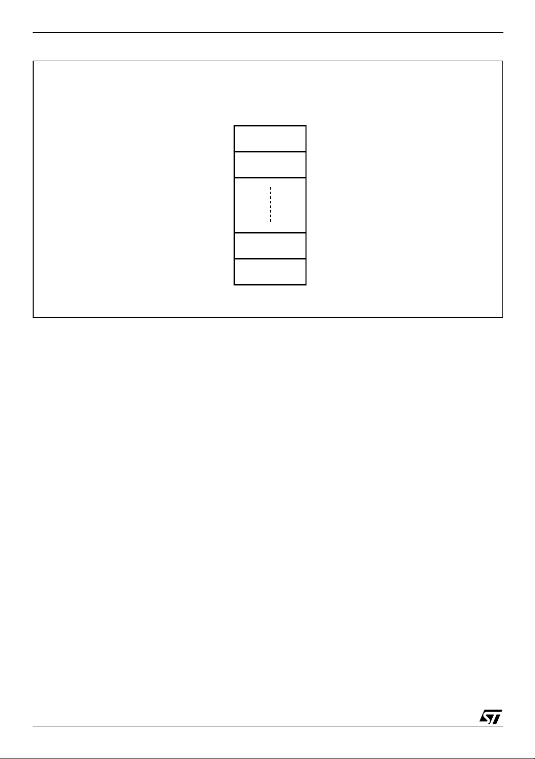
Figure 2. Logic Diagram
M58LW032A
A1-A21
V
PP
W
E
RP
V
V
DDQ
DD
21
16
DQ0-DQ15
M58LW032A
G
RB
R
L
K
V
V
SS
SSQ
AI04320
Table 1. Signal Names
A1-A21 Address inputs
DQ0-DQ15 Data Inputs/Outputs
E
G
K Clock
L
R Valid Data Ready
RB
RP
V
PP
W
V
DD
V
DDQ
V
SS
V
SSQ
NC Not Connected Internally
DU Do Not Use
Chip Enable
Output Enable
Latch Enable
Ready/Busy
Reset/Power-Down
Program/Erase Enable
Write Enable
Supply Voltage
Input/Output Supply Voltage
Ground
Input/Output Ground
7/61
M58LW032A
Figure 3. TSOP56 Connections
A21
A20
A19
A18
A17
A16
V
A15
A14
A13
A12
V
A11
A10
V
NC
DD
PP
RP
A9
A8
SS
A7
A6
A5
A4
A3
A2
A1
1
E
14
M58LW032A
15
28 29
56
43
42
NC
WR
G
RB
DQ15
DQ7
DQ14
DQ6
V
SS
DQ13
DQ5
DQ12
DQ4
V
DDQ
V
SSQ
DQ11
DQ3
DQ10
DQ2
V
DD
DQ9
DQ1
DQ8
DQ0
NC
K
NC
L
AI04321
8/61
Figure 4. TBGA64 Connections (Top view through package)
M58LW032A
87654321
A
B A19A2
C
D A16
E
F
G
A1
A4 A5
K
DU
A6 V
V
A7A3
DQ1
DQ0
DU
SS
A8
A10 A12
A11
DQ10
DQ2
PP
EA9
RP
DDQ
A13
A14
A15
DU
DQ4DQ3
DQ5V
V
DD
DU
DU
DU
DU
DU DU
DQ6
DQ15 RBDQ9DQ8
DQ14
A18
A20
DU
R
A21
A17
GDQ12DQ11
W
H
L
DU
V
DD
V
SSQ
DQ13
V
SS
DQ7
DU
AI04322
9/61
M58LW032A
Figure 5. Block Addresses
M58LW032A
Word (x16) Bus Width
Address lines A1-A21
1FFFFFh
1F8000h
1F7FFFh
1F0000h
00FFFFh
008000h
007FFFh
000000h
Note: Also see Appendix A, T able 25 for a full li st i ng of the Block Addresses
512 Kbit or
32 KWords
512 Kbit or
32 KWords
512 Kbit or
32 KWords
512 Kbit or
32 KWords
AI05500
10/61

SIGNAL DESCRIPTIONS
See Figure 2, Logic Diagram and Table 1, Signal
Names, for a brief overview of the signals connected to this device.
Address Inputs (A1-A21). The Address Inputs are used to select the cells to access in the memory array during Bus Read operations either to read or to program data to. During Bus Write operations they control the commands sent to the Command Interface of the internal state m ac hine. Chip Enable and Latch Enable must be low when selecting the addresses.
The address inputs are latched on the rising edge
of Chip Enable, Write Enable or Latch Enable,
whichever occurs first in a Write operation. The
address latch is transparent when Latch Enable is
low, V
. The address is internally latched in an
IL
Erase or Program operation. Data Inputs/Outputs (DQ0-DQ15). The Data In-
puts/Outputs output the data stored at the selected
address during a Bus Read operation, or are used
to input the data during a program operation. During Bus Write operations they repres ent the commands sent to the Command Interface of the
internal state machine. When used to input data or
Write commands they are latched on the rising
edge of Write Enable or Chip Enable, whichever
occurs first.
When Chip Enable and Output Enable are both
low, V
, the data bus outputs data from the mem-
IL
ory array, the Electronic Signature, the Block Protection status, the CFI Information or the contents
of the Status Register. The data bus is high impedance when the chip is deselected, Output E nable
is high, V
low, V
or the Reset/Power-Down signal is
IH,
. When the Program/Erase Controller is
IL
active the Ready/Busy status is given on DQ7.
Chip Enable (E
). The Chip Enable, E, input acti-
vates the memory control logic, input buffers, decoders and sense amplifiers. Chip Enable, E
V
deselects the memory and reduces the power
IH
consumption to the Standby level, I
Output Enable (G
). The Output Enable, G, gates
DD1
.
, at
the outputs through the data output buffers during
a read operation. When Output Enable, G
, is at V
IH
the outputs are high impedance. Output Enable,
G
, can be used to inhibit the data ou tput during a
burst read operation.
Write Enable (W
). The Write Enable input, W,
controls writing to the Command Interface, Input
Address and Data latches. Both addresses and
data can be latched on the rising edge of Write Enable (also see Latch Enable, L
Reset/Power-Down (RP
).
). The Reset/PowerDown pin can be used to apply a Hardware Reset
to the me mory.
M58LW032A
A Hardware Reset is achieved by holding Reset/
Power-Down Low, V
Reset/Power-Down is Low, V
, for at least t
IL
, the Status Regis-
IL
ter information is c leared and t he power consumption is reduced to power-down level. The device is
deselected and outputs are high impedance. If Reset/Power-Down goes low, V
,during a Block
IL
Erase, a Write to Buffe r and Program or a Block
Protect/Unprotect the operation is aborted and the
data may be corrupted. In this case the Ready/
Busy pin stays low, V
t
PLPH
+ t
until the completion of the Reset/
PHRH,
, for a ma ximum timin g of
IL
Power-Down pulse.
After Reset/Power-Down goes High, V
memory will be ready for Bus Read and Bus Write
operations after t
. Note that Ready/Busy
PHQV
does not fall during a reset , s ee Rea dy /Busy Ou tput section.
In an application, it is recommended to either associate the Reset/Power-Down pin, RP
reset signal of the microprocessor, or to ensure
that the Reset/Power-Down pin is kept Low during
Power-on. Otherwise, if a reset operation occurs
while the memory is performing an Erase or Pr ogram operation, the memory may output the Status Register information instead of being initialized
to the default Asynchronous Random Read.
Latch Enable (L
). The Bus Interface is config-
ured to latch the Address Inputs on the rising edge
of Latch Enable, L
. In synchronous bus operations
the address is latched on the active edge of the
Clock when Latch Enable is Low, V
IL
ing of Latch Enable, whichever occurs first. Once
latched, the addresses may change without affecting the address used by the memory. When Latch
Enable is Low, V
, the latch is transparent.
IL
Clo c k (K). The Clock, K, is used to synchronize the memory with the external bus during Synchronous Bus Read operations. The Clock can be configured to have an active rising or falling edge. Bus signals are latched on the active edge of the Clock during synchronous bus operations. In Synchronous Burst Read m ode the address is latched on the first active clock edge when Latch Enable is low, V
, or on the rising edge of Latch Enable,
IL
whichever occurs first.
During asynchronous bus operations the Clock is
not used. Valid Data Ready (R). The Valid Data Ready
output, R, is an open drain output that can be used
to identify if the memory is ready to output data or
not. The Valid Data Ready output is only active
during Synchronous Burst Read operat ions when
the Burst Length is set to Continuous. The Valid
Data Ready output can be configured to be active
on the clock edge of the invalid data read cycle or
. When
PLPH
, the
IH
, with the
or on the ris-
11/61

M58LW032A
one cycle before. Valid Data Ready Low, VOL, indicates that the data is not, or will not be valid. Valid Data Ready in a high-impedance state indicates
that valid data is or will be available.
Unless Synchronous Burst Read has been selected, Valid Data Ready is high-impedance. It may be
tied to other components with the same Valid Data
Ready signal to create a unique System Ready
signal.
The Valid Data Ready, R, output has an internal
pull-up resistor of approximately 1 MΩ powered
from V
, designers should use an external pull-
DDQ
up resistor of the correct value to meet the external
timing requirements for Valid Data Ready rising.
Refer to Figure 19.
Ready/Busy (RB
). The Ready/Busy output, RB,
is an open-drain output that can be used to identify
if the Program/Erase Controller is currently active.
When Ready/Busy is high impedance, the mem ory is ready for any Read, Program or Erase operation. Ready/Busy is Low, V
, during Program and
OL
Erase operations. When the device is busy it will
not accept any additional Program or Erase commands except Program/Erase Suspend. When the
Program/Erase Controller is idle, or suspended,
Ready Busy can float High through a pull-up resistor.
The use of an open-drain output allows the Ready/
Busy pins from several memories to be connected
to a single pull-up resistor. A Low will then indicate
that one, or more, of the memories is busy.
Ready/Busy is not Low during a reset unless the
reset was applied when the Program/Erase Con-
troller was active; Ready/Busy can rise before Reset/Power-Down rises.
Program/Erase Enable (VPP). The Program/ Erase Enable input, V
is used to protect all
PP,
blocks, preventing Program and Erase operations
from affecting their data.
Program/Erase Enable must be kept High during
all Program/Erase Controller operations, otherwise the operations is not guaranteed to suc ceed
and data may become corrupt.
Supply Voltage. VDD provides the power
V
DD
supply to the internal core of the memory device.
It is the main power supply for all operations
(Read, Program and Erase).
Supply Voltage. V
V
DDQ
provides the power
DDQ
supply to the I/O pins and enables all Outputs to
. V
be powered independently from V
tied to V
or can use a separate supply.
DD
DD
DDQ
can be
It is recommended to power-up and power-down
V
DD
and V
together to avoid any condition that
DDQ
would result in data corruption.
Ground. Ground, V
V
SS
is the reference for
SS,
the core power supply. It must be connected to the
system ground.
V
Ground. V
SSQ
the input/output circuitry driven by V
ground is the reference for
SSQ
DDQ
. V
SSQ
must be connected to VSS.
Note: Each device in a system should have
V
DD
and V
decoupled with a 0.1µF cerami c
DDQ
capacitor close to the pin (high frequency, inherently low inductance ca pacitors should b e
as close as possible to the package). See Figure 10, AC Measurement Load Circuit.
12/61

BUS OPERATIONS
There are 12 bus operations that control the memory. Each of these is described in this section, see
Tables 2 and 3, Bus Operat ions, for a summary.
The bus operation is selected through the Burst
Configuration Register; the bits in this register are
described at the end of this section.
On Power-up or after a Hardware Reset the memory defaults to Asynchrono us Latch Enable Controlled Read and Asynchronous Bus Write, no
other bus operation can be performed until the
Burst Control Register has been configured.
The Electronic Signature, CFI or Status Register
will be read i n asynchr onous m ode or single sy nchronous burst mode.
Typically glitches of less than 5ns on Chip Enable
or Write Enable are ignored by the memory and do
not affect bus operations.
Asynchronous Bus Operation s
For asynchronous bus operations refer to Tabl e 3
together with the text below.
Asynchronous Bus Read. Asynchronous Bus
Read operations read from the memory cells, or
specific registers (Electronic Signature, Status
Register, CFI and Block Prot ection Status) in the
Command Interface. A valid bus operation involves setting the desired address on the Address
Inputs, applying a Low signal, V
, to Chip Enable,
IL
Output Enable and Latch Enable and keeping
Write Enable High, V
. The Data Inputs/Outputs
IH
will output the value, see Figure 11, Asynchronous
Bus Read AC Waveforms, and Table 15, Asynchronous Bus Read AC Characteristics, for details
of when the output becomes valid.
Asynchronous Latch Controlled Bus Read.
Asynchronous Latch Controlled Bus Read operations read from the memory cells or specific registers in the Command Interface. The address is
latched in the memory before the value is ou tput
on the data bu s, allowing the address to cha nge
during the cycle without affecting the address that
the memo r y uses.
A valid bus operation i nvolves set ting the des ired
address on the Address Inputs, setting Chip Enable and Latch Enable Low, V
Enable High, V
; the address is latched on the ris-
IH
and keeping Write
IL
ing edge of Address L atch. Once latched, the Address Inputs can change. Set Output Enable Low,
V
, to read the data on the Data Inputs/Outputs;
IL
see Figure 12, Asynchronous Latch Controlled
Bus Read AC Waveforms and Table 16, Asynchronous Latch Controlled B us Read AC Characteristics for details on when the output becomes
valid.
Note that, since the Latch Enable input is transparent when set Low, V
, Asynchronous Bus Read
IL
M58LW032A
operations can be performed when the memory is
configured for Asynchronous Latch Enable bus
operations by holding Latch Enable Low, V
throughout the bus operation.
Asynchronous Page Read. Asynchronous Page
Read operations are used to read from several addresses within the same memory page. Each
memory page is 4 Wo rds and has the same A3A21, only A1 and A2 may change.
Valid bus operations are the same as Asynchronous Bus Read operations but with different timings. The first read operation within the page has
identical timings, subsequent reads within the
same page have much sh orter access t i mes. If the
page changes then the normal, longer timings apply again. See Figure 13, Asynchronous Page
Read AC Waveforms and Table 17, Asynchronous Page Read AC Characteristics for details on
when the outputs become valid.
Asynchronous Bus Write. Asynchronous Bus
Write operations write to the Command Interface
in order to send commands to the memory or to
latch addresses and in put data to program. Bus
Write operations are asynchronous, the clock, K,
is don’t care during Bus Write operations.
A valid Asynchronous Bus Write operation begins
by setting the desired address on the A ddress Inputs and setting Latch Enabl e Low, V
dress Inputs are latched by the Command
Interface on the rising edge of Chip Enable or
Write Enable, whichever occurs first. The Data Inputs/Outputs are la tched by the Comm and Interface on the rising edge of Chip Enable or Write
Enable, whichever occurs first. Output Enable
must remain High, V
, during the whole Asyn-
IH
chronous Bus Write operation. See Figures 14,
and 16, Asynchronous Write AC Wavef orms, and
Tables 18 and 19, Asynchronous Write and Latch
Controlled Write AC Characteristics, for details of
the timing requirements.
Asynchronous Latch Controlled Bus Write.
Asynchronous Latch Controlled Bus W rite operations write to the Command Interface in order to
send commands to the memory or to latch addresses and input data t o p rogram . Bus W r ite operations are asynchronous, the clock , K, is don’t
care during Bus Write operations.
A valid Asynchronous Latch Controlled Bus Write
operation begins by setting the desired address on
the Address Inputs and pulsing Latch Enable Low,
. The Address Inputs are latched b y the Com-
V
IL
mand Interface on the rising edge of Latch Enable,
Chip Enable or Write Enable, whichever occurs
first. The Data Inputs/Outputs are latched by the
Command Interface on the rising edge of Chip Enable or Write Enable, whichever occurs first. Ou t-
. The Ad-
IL
IL
13/61
M58LW032A
put Enable must remain High, VIH, during the
whole Asynchronous Bus Write operation. See
Figures 15 and 17 Asynchronous Latch Controlled
Write AC Waveforms, and Tables 18 and 19,
Asynchronous Write and Latch Controlled Write
AC Characteristics, for details of the timing requirements.
Output Disa bl e . The Data Inputs/Outputs are in the high impedance state when the Output Enable is High.
Standby. When Chip Enable is High, V
IH
, the
memory enters Standby mode and the Data Inputs/Outputs pins are placed in the high impedance state regardless of Output Enable or Write
Enable. The Supply Current is reduced to the
Standby Supply Current, I
DD1
.
During Program or Erase operations the memory
will continue to use the Program/Erase Supply
Current, I
til the operation completes.
Automatic Low Power. If there is no change in the state of the bus for a short period of time during Asynchronous Bus Re ad operations the memory enters Auto Low Pow er mode where the internal Supply Current is reduced to the Auto-Standby Supply Current, I still output data if a Bus Read operation is in progress.
Automatic Low Power is only available in Asynchronous Read modes.
Power-Down. The memory is in Power-Down mode when Reset/Power-Down, RP power consumption is reduced to the Power-Down level, I independent of Chip Enable, Output Enable or Write Enable.
Table 2. Asynchronous Bus Operations
Bus Operation Step E G W RP L A1-A21 DQ0-DQ15
V
Asynchronous Bus Read
Asynchronous Latch
Controlled Bus Read
Asynchronous Page Read
Asynchronous Bus Write
Asynchronous Latch
Controlled Bus Write
Output Disable
Standby
Power-Down X X X
Note: 1. X = Don’t Care VIL or VIH. High = VIH or VHH.
Address Latch
Read
Address Latch
V
IL
IL
V
V
IL
IL
V
V
IL
IL
V
V
IL
IL
V
V
IL
IH
V
V
IL
IH
V
V
IL
IH
V
X X High X X High Z
IH
, for Program or Erase operations un-
DD3
. The Data Inputs/Outputs will
DD5
, is Low. The
, and the out puts are high impedance,
DD2
V
High
IH
V
High
IH
V
High
IH
V
High
IH
V
High
IL
V
High
IL
V
High X X High Z
IH
V
V
V
V
V
V
V
IL
Address Data Output
IL
Address High Z
IL
IH
IL
IL
IL
X X High Z
X Data Output
Address Data Output
Address Data Input
Address Data Input
14/61
M58LW032A
Synchronous Bus Operations
For synchronous bus operat ions refer to Table 3
together with the text below.
Synchronous Burst Read. Synchronous Burst
Read operations are used to read from the memory at specific times synchronized to an external reference clock. The burst type, length and latency
can be configured. The different configurations for
Synchronous Burst Read operations are described in the Burst Configuration Register section.
A valid Synchronous Burst Read operation begins
when the address is set on the Address Inputs,
Write Enable is High, V
Latch Enable are Low, V
, and Chip Enable and
IH
, during the active edge
IL
of the Clock. The address is latched on the first active clock edge when Latch Enable i s low, or on
the rising edge of Latch Enable, whichever occurs
the X-latency specified in the Burst Control Register has expired. The output buffers are activated
by setting Output Enable Low, V
and 7 for exam ples of Synchronous Burst Read
operations.
In Continuous Burst mode one Burst Read operation can access the entire m emo ry sequ entially. If
the starting address is not associated with a page
(4 Word) boundary the V alid Data Ready, R, ou tput goes Low, V
be ready in time and additional wait-states are required. The Valid Data Ready output timing (bit
M8) can be changed in the Burst Configuration
Register.
The Synchronous Burst Read timing diagrams
and AC Characteristics a re described in the AC
and DC Parameters section. See Figures 18, 19
and Table 20.
first. The data becomes available for output after
Table 3. Synchronous Burst Read Bus Operations
Bus Operation Step E G RP
Address Latch
Synchronous Burst Read
Note: 1. X = Don't Care, VIL or VIH.
2. M15 = 0, Bit M 15 i s in the Burst Configuration Register.
3. T = trans i tion, see M6 in the Bu rst Configurat i on Register for details on the ac tive edge of K.
Read
Read Abort
V
V
V
X
IL
V
IL
X
IH
. See Figures 6
IL
, to indicate that the data will not
IL
(3)
K
V
IH
V
IL
IH
V
IH
L
V
T
T X Data Output
X X High Z
IL
A1-A21
DQ0-DQ15
Address Input
15/61

M58LW032A
Burst Configuration Register
The Burst Configuration Register is used to configure the type of bus access that the memory will
perform. The Burst Configuration Register bits are
described in Table 4. They specify the selection of
the burst length, burst type, burst X and Y latencies and the Read operation. See figures 6 and 7
for examples of Synchronous Burst Read configurations.
The Burst Configuration Register is set through
the Command Interface and will retain its information until it is re-configured, the device is reset, or
the device goes into Reset/Power-Down mode.
The Burst Configuration Register is read using the
Read Electronic Signature Command at addres s
05h.
Read Select Bit (M15). The Read Select bit,
M15, is used to switch between asynchronous and
synchronous Bus Read operations. When the
Read Select bit is set to ’1’, Bus Read operations
are asynchronous; when the Read Select but is
set to ’0’, Bus Read operations are synchronous.
On reset or power-up the Read Select bit is set to
’1’ for asynchronous access.
X-Latency Bits (M13-M11). The X-Latency bits are used during Synchronous Bus Read operations to set the number of clock cycles between the address being latched and the first data becoming available. For correct operation the X-Latency bits can only assume the values in Table 4, Burst Configuration Register.
Internal Clock Divider Bit (M10). The Internal
Clock Divider Bit is used to divide the internal clock
by two. When M10 is set to ‘1’ the internal clock is
divided by two, which effectively means that the X
and Y-Latency values are multiplied by two, that is
the number of clock cycles between the address
being latched and the first data becoming available will be twice the value set in M13-M11, and
the number of clock cycles between consecutive
reads will be twice the value set in M9. For example 8-1-1-1 will become 16-2-2-2. When M10 is set
to ‘0’ the internal clock runs n ormally and the X
and Y-Latency values are those s et in M13-M11
and M9.
Y-Latency Bit (M9). The Y-Latency bit is used
during Synchronous Bus Read operations to set
the number of clock cycles between consecutive
reads. The Y-Latency value depends on both the
X-Latency value and the setting in M9.
When the Y-Latency is 1 the data changes each
clock cycle; when the Y-Latency is 2 the data
changes every seco nd clock cycle. See Tab le 4,
Burst Configuration Register for valid combinations of the Y-Latency, the X-Latency and the
Clock frequency.
Valid Data Ready Bit (M8). The Valid Data Ready bit controls the timing of the Valid Data Ready output pin, R. When the Valid Data Ready bit is ’0’ the Valid Data Ready output pin is driven Low for the active clock edge when invalid data is output on the bus. When the Valid Data Ready bit is ’1’ the Valid Data Ready output pin is driven Low one clock cycle prior to invalid data being output on the bus.
Burst Type Bit ( M7 ). The Burst Type bit is used to configure the sequence of addresses read as sequential or interleaved. When the Burst Type bit is ’0’ the memory outputs from interleaved addresses; when the Burst Type bit is ’1’ the memory outputs from sequential addresses. See Tables 5, Burst Type Definition, for the sequence of addresses output from a given starting address in each mode.
Valid Clock Edge Bit (M6). The Valid Clock E dge bit, M6, is used to configure the active edge of the Clock, K, during Synchronous Burst Read operations. When the Valid Clock Edge bit is ’0’ the falling edge of the Clock is the active edge; when the Valid Clock Edge bit is ’1 ’ the rising edge of the Clock is active.
Burst Length Bit (M2-M0). The Burst Length bits set the maximum number of Words that can be output during a Synchronous Burst Read operation.
Table 4, Burst Configuration Register gives the
valid combinations of the Burst Length bits that the
memory accepts; Tables 5, Burst Type Definition,
give the sequence of addresses output from a given starting address for each length.
M5 M4 and M3 are reserved for future use.
16/61
Table 4. Burst Configuration Register
Address
Bit
Mnemonic Bit Name
16 M15 Read Select 1
15 M14 Reserved
Reset
Value
Value Description
0 Synchronous Burst Read
1 Asynchronous Bus Read (default at power-up)
001 Reserved
010
X-Latency = 4, 4-1-1-1 (use only with Y-Latency = 1)
M58LW032A
(1)
14
to
12
M13-M11
X-Latency
(2)
XXX
011
100
101
X-Latency = 5, 5-1-1-1, 5-2-2-2
X-Latency = 6, 6-1-1-1, 6-2-2-2
X-Latency = 7, 7-1-1-1, 7-2-2-2
110 X-Latency = 8, 8-1-1-1, 8-2-2-2
11 M10
10 M9
9M8
Clock Divider
Y-Latency
Valid Data
Ready
Internal
(3)
X
X
X
0 X and Y-Latencies remains as set in M13-M11 and M9
1 Divides internal clock, X and Y-Latencies multiplied by 2
0 Y-Latency = 1
1 Y-Latency = 2
0 R valid Low during valid Clock edge
1 R valid Low one cycle before valid Clock edge
0 Interleaved
8 M7 Burst Type X
1 Sequential
7M6
Valid Clock
Edge
X
0 Falling Clock edge
1 Rising Clock edge
6 to 4 M5-M3 Reserved
3
to
M2-M0 Burst Length XXX
1
Note: 1. 4 - 2 - 2 - 2 (represents X-Y-Y -Y ) is not allowed.
2. X latencies can be calculated as: (t
is the clock period).
3. Y latencies can be calcul ated as: t
4. t
SYSTEM MARGIN
is the time m argin requir ed for the calculation.
AVQV
KHQV
– t
LLKH
+ t
SYSTEM MARGIN
001 4 Words
010 8 Words
111 Continuous
+ t
) + t
QVKH
SYSTEM MARGIN
+ t
QVKH
< Y t
K.
< (X - 1) t
is an integer number from 4 to 8 and t
K. (X
K
17/61
M58LW032A
Tabl e 5. Burst Type Defi nition
Starting
Addressx4Sequentialx4Interleaved
x8
Sequential
x8
Interleaved
Continuous
0 0-1-2-3 0-1-2-3 0-1-2-3-4-5-6-7 0-1-2-3-4-5-6-7 0-1-2-3-4-5-6-7-8-9-10..
1 1-2-3-0 1-0-3-2 1-2-3-4-5-6-7-0 1-0-3-2-5-4-7-6 1-2-3-4-5-6-7-8-9-10-11..
2 2-3-0-1 2-3-0-1 2-3-4-5-6-7-0-1 2-3-0-1-6-7-4-5 2-3-4-5-6-7-8-9-10-11-12..
3 3-0-1-2 3-2-1-0 3-4-5-6-7-0-1-2 3-2-1-0-7-6-5-4 3-4-5-6-7-8-9-10-11-12-13..
4 – – 4-5-6-7-0-1-2-3 4-5-6-7-0-1-2-3 4-5-6-7-8-9-10-11-2-13-14..
5 – – 5-6-7-0-1-2-3-4 5-4-7-6-1-0-3-2 5-6-7-8-9-10-11-12-13-14..
6 – – 6-7-0-1-2-3-4-5 6-7-4-5-2-3-0-1 6-7-8-9-10-11-12-13-14-15..
7 – – 7-0-1-2-3-4-5-6 7-6-5-4-3-2-1-0 7-8-9-10-11-12-13-14-15-16..
8 – – – – 8-9-10-11-12-13-14-15-16-17..
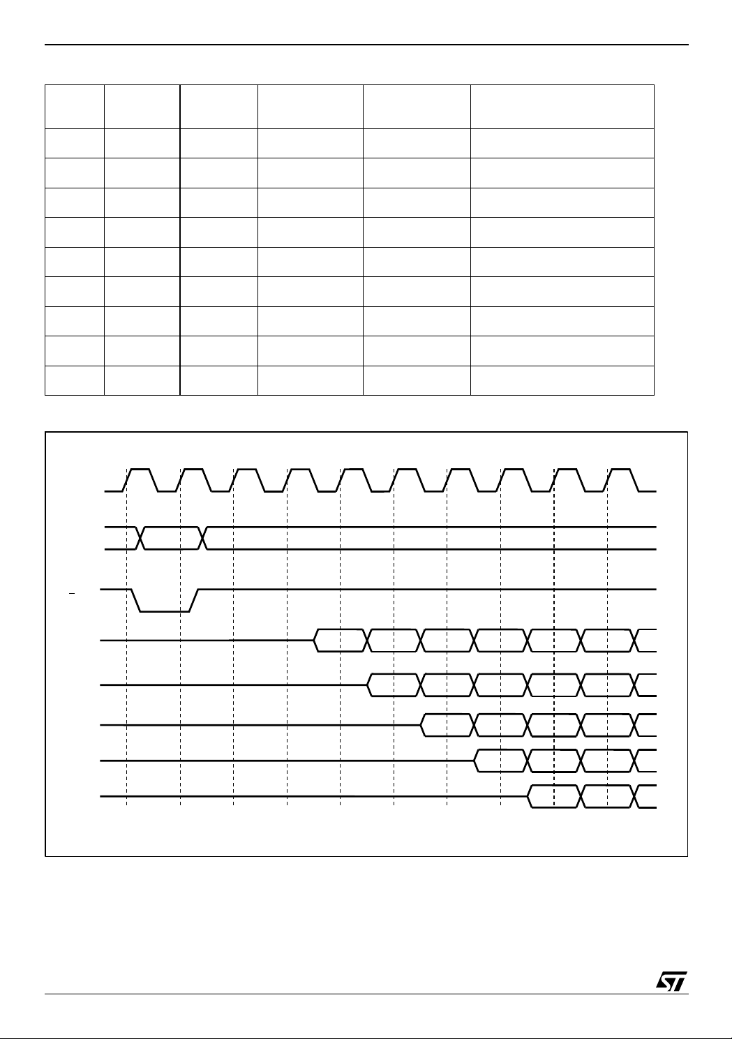
Figure 6. Burst Configuration X-1-1-1
0123456789
K
ADD
L
DQ
DQ
DQ
DQ
DQ
4-1-1-1
5-1-1-1
6-1-1-1
7-1-1-1
8-1-1-1
VALID
VALID
VALID
VALID
VALIDVALIDVALIDVALID
VALIDVALIDVALID
VALID
VALIDVALIDVALIDVALID
VALID
VALID
VALID
VALIDVALID
AI05512
18/61
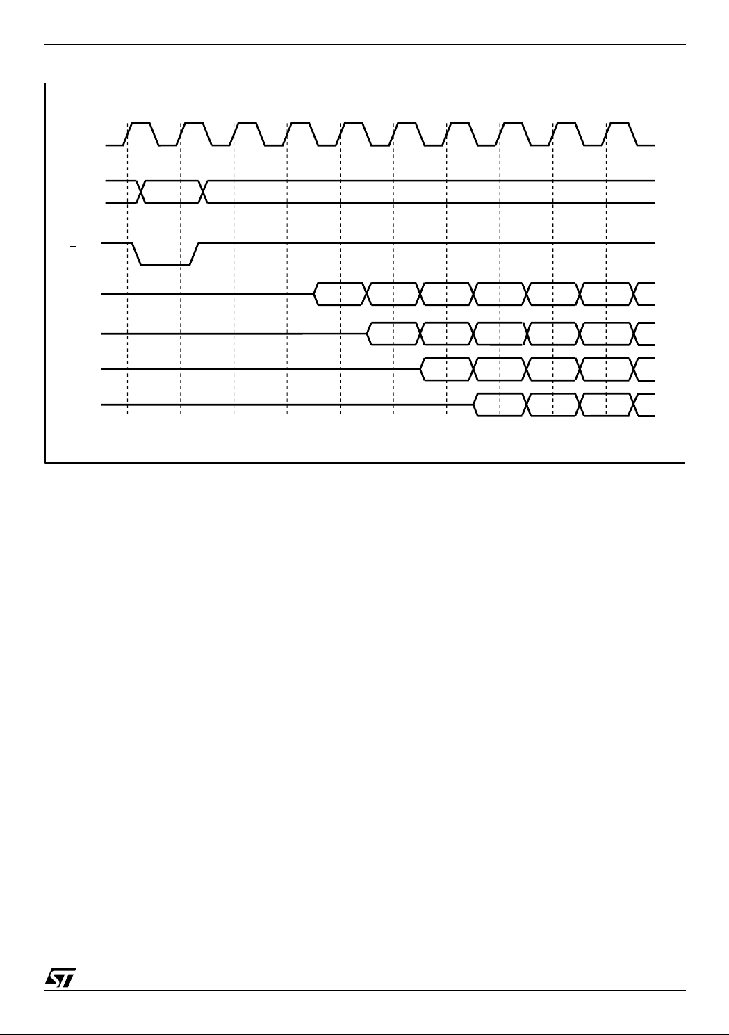
Figure 7. Burst Configuration X-2-2-2
0123456789
K
M58LW032A
ADD
L
DQ
DQ
DQ
DQ
5-2-2-2
6-2-2-2
7-2-2-2
8-2-2-2
VALID
NV
NV=NOT VALID
VALID
NV
NV
VALID
NV
VALID
NV
VALID
NV
VALID
NV
VALID
VALID
NV
VALID
NVNV
AI05513
19/61
 Loading...