

64 Mbit (4Mb x16 or 2Mb x32, Uniform Block, Burst)
FEATURES SUMMARY
■ WIDE DATA BUS for HIGH BANDWIDTH
– M58LV064 A: x16
– M58LV064 B: x16/x32
■ SUPPLY VOLTAGE
–V
–V
■ SYNCHRONOUS/ASYNCHRONOUS READ
– Synchronous Burst read
– Pipelined Synchronous Burst Read
– Asynchronous Random Read
– Asynchronous Ad dress Latch Control led
– Page Read
■ ACCESS TIME
– Synchronous Burst Read up to 66MHz
– Asynchronous Page Mode Read 150/25ns
– Random Read 150ns
■ PROGRAMMING TIME
– 16 Word or 8 Double-Word Write Buffer
–12µs Word effective programming time
■ 64 UNIFORM 64 KWord MEMORY BLOCKS
■ BLOCK PROTECTION/ UNPROTECTION
■ PROGRAM and ERASE SUSPEND
■ OTP SECURITY AREA
■ COMMON FLASH INTERFACE
■ 100,000 PROGRAM/ERASE CYCLES per
BLOCK
■ ELECTRONIC SIGNATURE
– Manufacturer Code: 0020h
– Device Code M58LV064A: 0015h
– Device Code M58LV064B: 0014h
= 3.0 to 3.6V M58LV064 core supply
DD
= 1.8 to VDD for I/O B u ffers
DDQ
Read
M58LV064A
M58LV064B
3V Supply Flash Memories
PRELIMINARY DATA
Figure 1. Packages
TSOP56 (N)
14 x 20mm
TBGA
TBGA64 (ZA)
10 x 13mm
TBGA
TBGA80 (ZA)
10 x13mm
December 2002
This is preliminary information on a new product now in development or undergoing evaluation. Details are subject to change without notice.
1/65

M58LV064A, M58LV064B
TABLE OF CONTENTS
SUMMARY DESCRIPTION. . . . . . . . . . . . . . . . . . . . . . . . . . . . . . . . . . . . . . . . . . . . . . . . . . . . . . . . . . . 6
Figure 2. Logic Diagram . . . . . . . . . . . . . . . . . . . . . . . . . . . . . . . . . . . . . . . . . . . . . . . . . . . . . . . . . 7
Table 1. Signal Names . . . . . . . . . . . . . . . . . . . . . . . . . . . . . . . . . . . . . . . . . . . . . . . . . . . . . . . . . . 7
Figure 3. TSOP56 Connections . . . . . . . . . . . . . . . . . . . . . . . . . . . . . . . . . . . . . . . . . . . . . . . . . . . . 8
Figure 4. TBGA64 Connections for M58LV064A (Top view through package) . . . . . . . . . . . . . . . . 9
Figure 5. TBGA80 Connections for M58LV064B (Top view through package) . . . . . . . . . . . . . . . 10
Figure 6. Block Addresses. . . . . . . . . . . . . . . . . . . . . . . . . . . . . . . . . . . . . . . . . . . . . . . . . . . . . . . 11
SIGNAL DESCRIPTIONS . . . . . . . . . . . . . . . . . . . . . . . . . . . . . . . . . . . . . . . . . . . . . . . . . . . . . . . . . . . 12
Address Inputs (A1-A22). . . . . . . . . . . . . . . . . . . . . . . . . . . . . . . . . . . . . . . . . . . . . . . . . . . . . . . . . 12
Data Inputs/Outputs (DQ0-DQ31). . . . . . . . . . . . . . . . . . . . . . . . . . . . . . . . . . . . . . . . . . . . . . . . . .12
Chip Enable (E). . . . . . . . . . . . . . . . . . . . . . . . . . . . . . . . . . . . . . . . . . . . . . . . . . . . . . . . . . . . . . . . 12
Output Enable (G). . . . . . . . . . . . . . . . . . . . . . . . . . . . . . . . . . . . . . . . . . . . . . . . . . . . . . . . . . . . . . 12
Write Enable (W). . . . . . . . . . . . . . . . . . . . . . . . . . . . . . . . . . . . . . . . . . . . . . . . . . . . . . . . . . . . . . . 12
Reset/Power-Down (RP). . . . . . . . . . . . . . . . . . . . . . . . . . . . . . . . . . . . . . . . . . . . . . . . . . . . . . . . . 12
Latch Enable (L).. . . . . . . . . . . . . . . . . . . . . . . . . . . . . . . . . . . . . . . . . . . . . . . . . . . . . . . . . . . . . . . 12
Clock (K).. . . . . . . . . . . . . . . . . . . . . . . . . . . . . . . . . . . . . . . . . . . . . . . . . . . . . . . . . . . . . . . . . . . . . 13
Burst Address Advance (B). . . . . . . . . . . . . . . . . . . . . . . . . . . . . . . . . . . . . . . . . . . . . . . . . . . . . . . 13
Valid Data Ready (R). . . . . . . . . . . . . . . . . . . . . . . . . . . . . . . . . . . . . . . . . . . . . . . . . . . . . . . . . . . . 13
Word Organization (WORD).. . . . . . . . . . . . . . . . . . . . . . . . . . . . . . . . . . . . . . . . . . . . . . . . . . . . . . 13
Ready/Busy (RB). . . . . . . . . . . . . . . . . . . . . . . . . . . . . . . . . . . . . . . . . . . . . . . . . . . . . . . . . . . . . . . 13
Program/Erase Enable (V
V
Supply Voltage. . . . . . . . . . . . . . . . . . . . . . . . . . . . . . . . . . . . . . . . . . . . . . . . . . . . . . . . . . . . . 13
DD
Input/Output Supply Voltage (V
Ground (V
Ground (V
). . . . . . . . . . . . . . . . . . . . . . . . . . . . . . . . . . . . . . . . . . . . . . . . . . . . . . . . . . . . . . . . . . 14
SS
). . . . . . . . . . . . . . . . . . . . . . . . . . . . . . . . . . . . . . . . . . . . . . . . . . . . . . . . . . . . . . . . . 14
SSQ
). . . . . . . . . . . . . . . . . . . . . . . . . . . . . . . . . . . . . . . . . . . . . . . . . . . . . . 13
PP
). . . . . . . . . . . . . . . . . . . . . . . . . . . . . . . . . . . . . . . . . . . . . . . . 14
DDQ
BUS OPERATIONS. . . . . . . . . . . . . . . . . . . . . . . . . . . . . . . . . . . . . . . . . . . . . . . . . . . . . . . . . . . . . . . . 15
Asynchronous Bus Operatio ns . . . . . . . . . . . . . . . . . . . . . . . . . . . . . . . . . . . . . . . . . . . . . . . . . . 15
Asynchronous Bus Read. . . . . . . . . . . . . . . . . . . . . . . . . . . . . . . . . . . . . . . . . . . . . . . . . . . . . . . . . 1 5
Asynchronous Latch Controlled Bus Read . . . . . . . . . . . . . . . . . . . . . . . . . . . . . . . . . . . . . . . . . . . 15
Asynchronous Page Read. . . . . . . . . . . . . . . . . . . . . . . . . . . . . . . . . . . . . . . . . . . . . . . . . . . . . . . . 15
Asynchronous Bus Write . . . . . . . . . . . . . . . . . . . . . . . . . . . . . . . . . . . . . . . . . . . . . . . . . . . . . . . . . 15
Asynchronous Latch Controlled Bus Write . . . . . . . . . . . . . . . . . . . . . . . . . . . . . . . . . . . . . . . . . . . 15
Output Disable. . . . . . . . . . . . . . . . . . . . . . . . . . . . . . . . . . . . . . . . . . . . . . . . . . . . . . . . . . . . . . . . . 16
Standby . . . . . . . . . . . . . . . . . . . . . . . . . . . . . . . . . . . . . . . . . . . . . . . . . . . . . . . . . . . . . . . . . . . . . . 16
Automatic Low Power.. . . . . . . . . . . . . . . . . . . . . . . . . . . . . . . . . . . . . . . . . . . . . . . . . . . . . . . . . . . 16
Power-Down.. . . . . . . . . . . . . . . . . . . . . . . . . . . . . . . . . . . . . . . . . . . . . . . . . . . . . . . . . . . . . . . . . . 16
Table 2. Asynchronous Bus Operations . . . . . . . . . . . . . . . . . . . . . . . . . . . . . . . . . . . . . . . . . . . . 16
Synchronous Bus Operations . . . . . . . . . . . . . . . . . . . . . . . . . . . . . . . . . . . . . . . . . . . . . . . . . . .17
Synchronous Burst Read. . . . . . . . . . . . . . . . . . . . . . . . . . . . . . . . . . . . . . . . . . . . . . . . . . . . . . . . . 17
Synchronous Pipelined Burst Read. . . . . . . . . . . . . . . . . . . . . . . . . . . . . . . . . . . . . . . . . . . . . . . . .17
Synchronous Burst Read Suspend . . . . . . . . . . . . . . . . . . . . . . . . . . . . . . . . . . . . . . . . . . . . . . . . . 17
2/65

M58LV064A, M58LV064B
Table 3. Synchronous Burst Read Bus Operations. . . . . . . . . . . . . . . . . . . . . . . . . . . . . . . . . . . . 18
Table 4. Address Latch Cycle for Optimum Pipelined Synchronous Burst Read . . . . . . . . . . . . . 18
Figure 7. Synchronous Burst Read Operation. . . . . . . . . . . . . . . . . . . . . . . . . . . . . . . . . . . . . . . . 19
Figure 8. Example Synchronous Pipelined Burst Read Operation . . . . . . . . . . . . . . . . . . . . . . . . 19
Figure 9. Example Burst Address Advance and Burst Abort operations. . . . . . . . . . . . . . . . . . . . 20
Burst Configurat io n Regist er. . . . . . . . . . . . . . . . . . . . . . . . . . . . . . . . . . . . . . . . . . . . . . . . . . . . 21
Read Select Bit (M15) . . . . . . . . . . . . . . . . . . . . . . . . . . . . . . . . . . . . . . . . . . . . . . . . . . . . . . . . . . . 21
X-Latency Bits (M14-M11). . . . . . . . . . . . . . . . . . . . . . . . . . . . . . . . . . . . . . . . . . . . . . . . . . . . . . . . 2 1
Y-Latency Bit (M9). . . . . . . . . . . . . . . . . . . . . . . . . . . . . . . . . . . . . . . . . . . . . . . . . . . . . . . . . . . . . .21
Valid Data Ready Bit (M8). . . . . . . . . . . . . . . . . . . . . . . . . . . . . . . . . . . . . . . . . . . . . . . . . . . . . . . . 21
Burst Type Bit (M7).. . . . . . . . . . . . . . . . . . . . . . . . . . . . . . . . . . . . . . . . . . . . . . . . . . . . . . . . . . . . . 21
Valid Clock Edge Bit (M6).. . . . . . . . . . . . . . . . . . . . . . . . . . . . . . . . . . . . . . . . . . . . . . . . . . . . . . . . 21
Latch Enable Bit (M3) . . . . . . . . . . . . . . . . . . . . . . . . . . . . . . . . . . . . . . . . . . . . . . . . . . . . . . . . . . . 21
Burst Length Bit (M2-M0). . . . . . . . . . . . . . . . . . . . . . . . . . . . . . . . . . . . . . . . . . . . . . . . . . . . . . . . . 21
Table 5. Burst Conf iguration Registe r. . . . . . . . . . . . . . . . . . . . . . . . . . . . . . . . . . . . . . . . . . . . . . 22
Table 6. Burst Type Definition (x16 Bus Width). . . . . . . . . . . . . . . . . . . . . . . . . . . . . . . . . . . . . . . 23
Table 7. Burst Type Definition (x32 Bus Width). . . . . . . . . . . . . . . . . . . . . . . . . . . . . . . . . . . . . . . 23
Table 8. Burst Performance. . . . . . . . . . . . . . . . . . . . . . . . . . . . . . . . . . . . . . . . . . . . . . . . . . . . . . 24
COMMAND INTERFACE . . . . . . . . . . . . . . . . . . . . . . . . . . . . . . . . . . . . . . . . . . . . . . . . . . . . . . . . . . . 25
Read Memory Array Command. . . . . . . . . . . . . . . . . . . . . . . . . . . . . . . . . . . . . . . . . . . . . . . . . . . .25
Read Electronic Signature Comma nd . . . . . . . . . . . . . . . . . . . . . . . . . . . . . . . . . . . . . . . . . . . . . . . 25
Read Query Command. . . . . . . . . . . . . . . . . . . . . . . . . . . . . . . . . . . . . . . . . . . . . . . . . . . . . . . . . . . 25
Read Status Register Command. . . . . . . . . . . . . . . . . . . . . . . . . . . . . . . . . . . . . . . . . . . . . . . . . . .25
Clear Status Regist e r Command. . . . . . . . . . . . . . . . . . . . . . . . . . . . . . . . . . . . . . . . . . . . . . . . . . . 25
Block Erase Command . . . . . . . . . . . . . . . . . . . . . . . . . . . . . . . . . . . . . . . . . . . . . . . . . . . . . . . . . . 2 5
Write to Buffer and Program Command.. . . . . . . . . . . . . . . . . . . . . . . . . . . . . . . . . . . . . . . . . . . . . 25
Program/Erase Suspend Comm and . . . . . . . . . . . . . . . . . . . . . . . . . . . . . . . . . . . . . . . . . . . . . . . . 26
Program/Eras e Resume Command . . . . . . . . . . . . . . . . . . . . . . . . . . . . . . . . . . . . . . . . . . . . . . . . 26
Set Burst Configuration Register Command. . . . . . . . . . . . . . . . . . . . . . . . . . . . . . . . . . . . . . . . . . 27
Block Protect Command.. . . . . . . . . . . . . . . . . . . . . . . . . . . . . . . . . . . . . . . . . . . . . . . . . . . . . . . . . 27
Blocks Unprotect Command.. . . . . . . . . . . . . . . . . . . . . . . . . . . . . . . . . . . . . . . . . . . . . . . . . . . . . . 27
Table 9. Commands . . . . . . . . . . . . . . . . . . . . . . . . . . . . . . . . . . . . . . . . . . . . . . . . . . . . . . . . . . . 28
Table 10. Read Electronic Signature. . . . . . . . . . . . . . . . . . . . . . . . . . . . . . . . . . . . . . . . . . . . . . . 28
Table 11. Program, Erase Times and Program Erase Endurance Cycles . . . . . . . . . . . . . . . . . . 29
STATUS REGISTER. . . . . . . . . . . . . . . . . . . . . . . . . . . . . . . . . . . . . . . . . . . . . . . . . . . . . . . . . . . . . . . 30
Program/Erase Controller Status (Bit 7) . . . . . . . . . . . . . . . . . . . . . . . . . . . . . . . . . . . . . . . . . . . . .30
Erase Suspend Status (Bit 6) . . . . . . . . . . . . . . . . . . . . . . . . . . . . . . . . . . . . . . . . . . . . . . . . . . . . . 30
Erase Status (Bit 5). . . . . . . . . . . . . . . . . . . . . . . . . . . . . . . . . . . . . . . . . . . . . . . . . . . . . . . . . . . . . 30
Program Status (Bit 4). . . . . . . . . . . . . . . . . . . . . . . . . . . . . . . . . . . . . . . . . . . . . . . . . . . . . . . . . . . 30
VPP Status (Bit 3) . . . . . . . . . . . . . . . . . . . . . . . . . . . . . . . . . . . . . . . . . . . . . . . . . . . . . . . . . . . . . . 31
Program Suspend Status (Bit 2) . . . . . . . . . . . . . . . . . . . . . . . . . . . . . . . . . . . . . . . . . . . . . . . . . . . 31
Block Protection Status (Bit 1). . . . . . . . . . . . . . . . . . . . . . . . . . . . . . . . . . . . . . . . . . . . . . . . . . . . . 3 1
Reserved (Bit 0). . . . . . . . . . . . . . . . . . . . . . . . . . . . . . . . . . . . . . . . . . . . . . . . . . . . . . . . . . . . . . . . 31
3/65

M58LV064A, M58LV064B
Table 12. Statu s Regi ster Bits. . . . . . . . . . . . . . . . . . . . . . . . . . . . . . . . . . . . . . . . . . . . . . . . . . . . 32
MAXIMUM RATING. . . . . . . . . . . . . . . . . . . . . . . . . . . . . . . . . . . . . . . . . . . . . . . . . . . . . . . . . . . . . . . . 33
Table 13. Absolu te Maximum Ratings. . . . . . . . . . . . . . . . . . . . . . . . . . . . . . . . . . . . . . . . . . . . . . 33
DC and AC PARAMETERS . . . . . . . . . . . . . . . . . . . . . . . . . . . . . . . . . . . . . . . . . . . . . . . . . . . . . . . . . 34
Table 14. Operating and AC Measurement Conditions. . . . . . . . . . . . . . . . . . . . . . . . . . . . . . . . . 34
Figure 10. AC Measurement Input Output Waveform . . . . . . . . . . . . . . . . . . . . . . . . . . . . . . . . . . 34
Figure 11. AC Measure men t L o ad Circuit. . . . . . . . . . . . . . . . . . . . . . . . . . . . . . . . . . . . . . . . . . . 34
Table 15. Capacitance. . . . . . . . . . . . . . . . . . . . . . . . . . . . . . . . . . . . . . . . . . . . . . . . . . . . . . . . . . 34
Table 16. DC Characte r istics. . . . . . . . . . . . . . . . . . . . . . . . . . . . . . . . . . . . . . . . . . . . . . . . . . . . . 35
Figure 12. Asynchronous Bus Read AC Waveforms. . . . . . . . . . . . . . . . . . . . . . . . . . . . . . . . . . . 36
Table 17. Asynchronous Bus Read AC Characteristics. . . . . . . . . . . . . . . . . . . . . . . . . . . . . . . . . 36
Figure 13. Asynchronous Latch Controlled Bus Read AC Waveforms . . . . . . . . . . . . . . . . . . . . . 37
Table 18. Asynchronous Latch Controlled Bus Read AC Characteristics. . . . . . . . . . . . . . . . . . . 37
Figure 14. Asynchronous Page Read AC Waveforms . . . . . . . . . . . . . . . . . . . . . . . . . . . . . . . . . 38
Table 19. Asynchronous Page Read AC Characteristics . . . . . . . . . . . . . . . . . . . . . . . . . . . . . . . 38
Figure 15. Asynchronous Write AC Waveform, Write Enable Controlled . . . . . . . . . . . . . . . . . . . 39
Figure 16. Asynchronous Latch Controlled Write AC Waveform, Write Enable Controlled. . . . . . 39
Table 20. Asynchronous Write and Latch Controlled Write AC Characteristics, Write Enable
Controlled.. . . . . . . . . . . . . . . . . . . . . . . . . . . . . . . . . . . . . . . . . . . . . . . . . . . . . . . . . . . . . . . . . . . 40
Figure 17. Asynchronous Write AC Waveforms, Chip Enable Controlled. . . . . . . . . . . . . . . . . . . 41
Figure 18. Asynchronous Latch Controlled Write AC Waveforms, Chip Enable Controlled . . . . . 41
Table 21. Asynchronous Write and Latch Controlled Write AC Characteristics, Chip Enable
Controlled . . . . . . . . . . . . . . . . . . . . . . . . . . . . . . . . . . . . . . . . . . . . . . . . . . . . . . . . . . . . . . . . . . . 42
Figure 19. Synchronous Burst Read AC Waveform . . . . . . . . . . . . . . . . . . . . . . . . . . . . . . . . . . . 43
Figure 20. Synchronous Burst Read - Continuous - Valid Data Ready Output. . . . . . . . . . . . . . . 44
Table 22. Synch r o nous Bu r st Read AC Characteristi cs . . . . . . . . . . . . . . . . . . . . . . . . . . . . . . . . 45
Figure 21. Reset , Po wer-Down and Power-up AC Waveform. . . . . . . . . . . . . . . . . . . . . . . . . . . . 46
Table 23. Reset, Power-Down and Power-up AC Characteristics . . . . . . . . . . . . . . . . . . . . . . . . 46
PACKAGE MECHANICAL . . . . . . . . . . . . . . . . . . . . . . . . . . . . . . . . . . . . . . . . . . . . . . . . . . . . . . . . . . 47
Figure 22. TSOP56 - 56 lead Plastic Thin Small Outline, 14 x 20 mm, Package Outline . . . . . . . 47
Table 24. TSOP56 - 56 lead Plastic Thin Small Outline, 14 x 20 mm, Package Mechanical Data 47
Figure 23. TBGA64 - 10x13mm, 8 x 8 ball array 1mm pitch, Package Outline. . . . . . . . . . . . . . . 48
Table 25. TBGA64 - 10x13mm, 8 x 8 ball array, 1 mm pitch, Package Mechanical Data. . . . . . . 48
Figure 24. TBGA80 - 10x13mm, 8 x 10 ball array, 1mm pitch, Package Outline . . . . . . . . . . . . . 49
Table 26. TBGA80 - 10x13mm, 8 x 10 ball array, 1mm pitch, Package Mechanical Data . . . . . . 49
PART NUMBERING. . . . . . . . . . . . . . . . . . . . . . . . . . . . . . . . . . . . . . . . . . . . . . . . . . . . . . . . . . . . . . 50
Table 27. Ordering Information Scheme. . . . . . . . . . . . . . . . . . . . . . . . . . . . . . . . . . . . . . . . . . . . 50
APPENDIX A. BLOCK ADDRESS TABLE. . . . . . . . . . . . . . . . . . . . . . . . . . . . . . . . . . . . . . . . . . . . . 51
Table 28. Block Addresses . . . . . . . . . . . . . . . . . . . . . . . . . . . . . . . . . . . . . . . . . . . . . . . . . . . . . . 51
APPENDIX B. COMMON FLASH INTERFACE - CFI. . . . . . . . . . . . . . . . . . . . . . . . . . . . . . . . . . . . . 52
4/65

M58LV064A, M58LV064B
Table 29. Query Stru cture Overview. . . . . . . . . . . . . . . . . . . . . . . . . . . . . . . . . . . . . . . . . . . . . . . 52
Table 30. CFI - Query Addre ss an d Data Outpu t . . . . . . . . . . . . . . . . . . . . . . . . . . . . . . . . . . . . . 53
Table 31. CFI - Device Volt age and Ti mi n g Speci fi ca tion. . . . . . . . . . . . . . . . . . . . . . . . . . . . . . . 54
Table 32. Device Geo metry Definitio n. . . . . . . . . . . . . . . . . . . . . . . . . . . . . . . . . . . . . . . . . . . . . . 55
Table 33. Block Status Register . . . . . . . . . . . . . . . . . . . . . . . . . . . . . . . . . . . . . . . . . . . . . . . . . . 55
Table 34. Extended Query information . . . . . . . . . . . . . . . . . . . . . . . . . . . . . . . . . . . . . . . . . . . . . 56
APPENDIX C. FLOW CHARTS . . . . . . . . . . . . . . . . . . . . . . . . . . . . . . . . . . . . . . . . . . . . . . . . . . . . . 57
Figure 25. Write to Buffer and Program Flowchart and Pseudo Code . . . . . . . . . . . . . . . . . . . . . 57
Figure 26. Program Suspend & Resume Flowchart and Pseudo Code . . . . . . . . . . . . . . . . . . . . 58
Figure 27. Erase Flowchart and Pseudo Code . . . . . . . . . . . . . . . . . . . . . . . . . . . . . . . . . . . . . . . 59
Figure 28. Erase Suspend & Resume Flowchart and Pseudo Code. . . . . . . . . . . . . . . . . . . . . . . 60
Figure 29. Command Interface and Program Erase Controller Flowchart (a). . . . . . . . . . . . . . . . 61
Figure 30. Command Interface and Program Erase Controller Flowchart (b). . . . . . . . . . . . . . . . 62
Figure 31. Command Interface and Program Erase Controller Flowchart (c) . . . . . . . . . . . . . . . . 63
REVISION HISTORY . . . . . . . . . . . . . . . . . . . . . . . . . . . . . . . . . . . . . . . . . . . . . . . . . . . . . . . . . . . . . . . 64
Table 35. Document Revision History. . . . . . . . . . . . . . . . . . . . . . . . . . . . . . . . . . . . . . . . . . . . . . 64
5/65

M58LV064A, M58LV064B
SUMMARY DESCRIPTION
M58LV064 is a 64Mbit (4Mb x16 or 2Mb x32) nonvolatile memory that can be read, erased and reprogrammed. These operations can be performed
using a single low voltage (2.7V to 3.6V) core supply. On power-up the memory default to Read
mode with an asynchronous bus where it can be
read in the same way as a non-burst Flash memory.
The memory is divided into 64 blocks of 1Mbit that
can be erased i ndependently so it is poss ible to
preserve valid data while old data is erased. P rogram and Erase commands are written to the
Command Interface of the memory. An on-chip
Program/Erase Controller simplifies the process of
programming or erasing the memory by taking
care of all of the special operations that are required to update the memory contents. The end of
a Program or Erase operation can be detected and
any error conditions identified in the Status Register. The command set required to control the
memory is consistent with JEDEC standards.
The Write Buffer allows the microprocessor to program from 4 to 16 Words (or from 2 to 8 Doub le
Words) in parallel, both speeding up the programming and freeing up the microprocessor to perform
other work. The minimum buffer size for a program
operation is a 4 Word (or 2 Double Word) page. A
page can only be programmed once between
Erase operations.
Erase can be suspended in order to perform either
Read or Program in any other block and then resumed. Program ca n be s uspended to Read data
in any other block and then resum ed. Eac h block
can be programmed and erased over 100,000 cycles.
Individual block protection against Program or
Erase is provided for data security. All blocks are
protected during power-up. The protection of the
blocks is non-volatile; after power-up the protec-
tion status of each block is restored to the state
when power was last removed. Software commands are provided to allow protection of some or
all of the blocks and to cancel all block protection
bits simultaneously. All Program o r Erase operations are blocked when the Program Erase Enable
input Vpp is low.
The Reset/Power-Down pin is used to apply a
Hardware Reset to the memory and to set the device in deep power-down mode. It can also be
used to temporarily disable the prot ect ion mec hanism.
In asynchronous mode Chip Enable, Output Enable and Write Enable signals control the bus operation of the memory. An Address Latch input can
be used to latch addresses in Latch Controlled
mode. Together they allow simple, yet powe rful,
connection to most microprocessors, often without
additional logic.
In synchronous mode all Bus Read operations are
synchronous with the Clock. Chip Enable and Output Enable select the Bus Read operation; the address is Latched using the Latch Enable inputs
and the address is advanced using Burst Address
Advance. The signals are compatible with most
microprocessor burst interfaces.
A One Time Programmable (OTP) area is included
for security purposes. Either 1K W ords (x16 Bus
Width) or 1K Double-Words (x32 Bus Width) is
available in the OTP area. The proc ess o f reading
from and writing to the OTP area is not published
for security purposes; contact STMicroelectronics
for details on how to use the OTP area.
The memory is offered in various packages . The
M58LV064A is available in TSOP56 (14 x 20 mm)
and TBGA64 (1mm pitch). The M58LV064B is
available in TBGA80 (1mm pitch).
6/65
M58LV064A, M58LV064B
Figure 2. Logic Diagram
V
V
DDQ
DD
22
A1-A22
V
PP
W
E
G
RP
L
B
K
(1)
WORD
Note: 1. M 58LV064B on l y.
M58LV064A
M58LV064B
V
V
SS
SSQ
16
16
DQ0-DQ15
DQ16-DQ31
RB
R
AI03223b
Table 1. Signal Names
A1 Address Input (x16 Bus Width only)
A2-A22 Address inputs
DQ0-DQ15 Data Inputs/Outputs
DQ16-DQ31
(1)
B
E
G
K Clock
L
R Valid Data Ready
RB
RP
V
PP
W Write Enable
WORD
V
DD
V
DDQ
V
SS
V
SSQ
NC Not Connected Internally
Data Inputs/Outputs (x32 Bus Width of
M58LV064B only)
Burst Address Advance
Chip Enable
Output Enable
Latch Enable
Ready/Busy
Reset/Power-Down
Program/Erase Enable
Word Organization (M58LV064B only)
Supply Voltage
Input/Output Supply Voltage
Ground
Input/Output Ground
7/65
M58LV064A, M58LV064B
Figure 3. TSOP56 Connections
A22
A21
A20
A19
A18
A17
A16
V
A15
A14
A13
A12
V
A11
A10
V
DD
PP
RP
A9
A8
SS
A7
A6
A5
A4
A3
A2
A1
1
R
E
14
M58LV064A
15
28 29
56
43
42
NC
W
G
RB
DQ15
DQ7
DQ14
DQ6
V
SSQ
DQ13
DQ5
DQ12
DQ4
V
DDQ
V
SS
DQ11
DQ3
DQ10
DQ2
V
DD
DQ9
DQ1
DQ8
DQ0
B
K
NC
L
AI03224b
8/65
M58LV064A, M58LV064B
Figure 4. TBGA64 Connections for M58LV064A (To p view thro ugh package)
87654321
A
B RA19A2
C
D A16
E
F
G
A1
V
A4 A5
DQ1
K
NC
DQ0
A6 V
SS
A7A3
A8
A10 A12
A11
DQ10
DQ2B
PP
EA9
RP
DDQ
A13
A14
A15
NC
DQ4DQ3
DQ5V
V
DD
NC
NC
NC
NC
NC NC
DQ6
DQ15 RBDQ9DQ8
DQ14
A20
A22A18
A21
A17
GDQ12DQ11
W
H
L
NC
V
DD
V
SS
DQ13
V
SSQ
DQ7
NC
AI03536
9/65
M58LV064A, M58LV064B
Figure 5. TBGA80 Connections for M58LV064B (To p view thro ugh package)
87654321
A
B RA19A2
C
D NC
E
F
G
H
A1
A4 A5
DQ24
K DQ15DQ2 DQ12B DQ11 GRB
A8 A22A18
A7
A6A3
DQ18
V
SS
A10
A11
DQ27
LDQ17 DQ26 DQ30DQ5DQ3
A12A9
V
RP
E
PP
A13
A14
A15
NC NC
V
DD
A16
A17
DQ28
DQ20 DQ29
W DQ21
A20
DQ22 DQ31DQ19DQ16 DQ25 DQ6WORD
A21
NC
DQ23DQ13DQ10
10/65
J
K
DQ0
DQ8
DQ1
DQ9 DQ14
V
DD
V
DD
SS
V
SS
V
DQ4V
DDQ
V
V
SSQ
DDQ
V
V
SSQ
DDQ
DQ7
AI03983
Figure 6. Block Addresses
M58LV064A, M58LV064B
M58LV064A, M58LV064B
Word (x16) Bus Width
Address lines A1-A22
3FFFFFh
3F0000h
3EFFFFh
3E0000h
01FFFFh
010000h
00FFFFh
000000h
Note: Also see Appendix A, Table 28 for a full l i st i ng of the Block Addresses
1 Mbit or
64 KWords
1 Mbit or
64 KWords
Total of 64
1 Mbit Blocks
1 Mbit or
64 KWords
1 Mbit or
64 KWords
M58LV064B
Double-Word (x32) Bus Width
Address lines A2-A22
(A1 is Don't Care)
1FFFFFh
1F8000h
1F7FFFh
1F0000h
00FFFFh
008000h
007FFFh
000000h
1 Mbit or
32 KDouble-Words
1 Mbit or
32 KDouble-Words
1 Mbit or
32 KDouble-Words
1 Mbit or
32 KDouble-Words
AI03228b
11/65

M58LV064A, M58LV064B
SIGNAL DESCRIPTIONS
See Figure 2, Logic Diagram and Table 1, Signal
Names, for a brief overview of the signals connected to this de vice.
Address Inputs (A1-A22). The Address Inputs
are used to select the cells to access in the memory array during Bus Read operations either to
read or to program data to. During Bus Write operations they control the commands sent to the
Command Interface of the internal state m ac hine.
Chip Enable must be low when selecting the addresses.
The address inputs are latched on the rising edge
of Chip Enable, Write Enable or Latch Enable,
whichever occurs first in a Write operation. The
address latch is transparent when Latch Enable is
low, V
Erase or Program operation.
With a x32 Bus Width, WORD
put A1 is ignored; the Least Significant Word is
output on DQ0-DQ15 and the Most Significant
Word is output on DQ16-DQ31. With a x16 Bus
Width, WORD
output on DQ0-DQ15 when A1 is low, V
Most Significant Word is output on DQ0-DQ15
when A1 is high, V
Data Inputs/Outputs (DQ0-DQ31). The Data Inputs/Outputs output the data stored at the selected
address during a Bus Read operation, or are used
to input the data during a program operation. During Bus Write operations they represent the commands sent to the Command Interface of the
internal state machine. When used to input data or
Write commands they are latched on the rising
edge of Write Enable or Chip Enable, whichever
occurs first.
When Chip Enable and Output Enable are both
low, V
ory array, the Electronic Signature, the Block Protection status, the CFI Information or the contents
of the Status Register. The data bus is high impedance when the chip is deselected, Output Enab le
is High, V
Low, V
active the Ready/Busy status is given on DQ7
while DQ0-DQ6 and DQ8-DQ 31 are high impedance.
With a x16 Bus Width, WORD
are not used and are high impedance.
Chip Enable (E
vates the memory control logic, input bu ffers, decoders and sense amplifiers. Chip Enable, E
V
consumption to the Standby level, I
Output Enable (G
the outputs through the data output buffers during
a read operation. When Output Enable, G
. The address is internally latched in an
IL
= VIH, Address In-
= VIL, the Least Significant Word is
and the
IL,
.
IH
, the data bus outputs data from the mem-
IL
or the Reset/Power-Down signal is
IH,
. When the Program/Erase Controller is
IL
= VIL, DQ16-DQ31
). The Chip Enable, E, input a cti-
deselects the memory and reduces the power
IH
DD1
.
). The Output Enable, G, gates
, is at V
, at
the outputs are high impedance. Output Enable,
, can be used to inhibit the data ou tput during a
G
burst read operation.
Write Enable (W
). The Write Enable input, W,
controls writing to the Command Interface, Input
Address and Data latches. Both addresses and
data can be latched on the rising edge of Wri te Enable (also see Latch Enable, L
Reset/Power-Down (RP
).
). The Reset/PowerDown pin can be used to apply a Hardware Reset
to the memory or to temporarily unprotect all
blocks that have been pr ote cte d .
A Hardware Reset is achieved by holding Reset/
Power-Down Low, V
Reset/Power-Down is Low, V
, for at least t
IL
, the Status Regis-
IL
ter information is cleared and the power consumption is reduced to deep power-down level. The
device is deselected and outputs are high impedance. If Reset/Power-Down goes low, V
Block Erase, a Write to Buffe r and Program or a
Block Protect/Unprotect the operat ion is aborted
and the data may be corrupted. In this case the
Ready/Busy pin stays low, V
ing of t
PLPH
+ t
until the completion of the Re-
PHRH,
, for a maximum tim-
IL
set/Power-Down pulse.
After Reset/Power-Down goes High, V
memory will be ready for Bus Read and Bus Write
operations after t
PHEL
or t
, whichever occurs
RHEL
last. Note that Ready/Busy does not fall during a
reset, see Ready/Busy Outp ut sect i on.
During power-up Reset/Power-Down must be held
Low, V
Furthermore it must stay low for t
IL.
after the Supply Voltage inputs become stable.
The device will then be configured in Asynchronous Random Read mode.
See Table 23 and F igure 21, Reset , Po wer-Down
and Power-up Characteristics, for more details.
Holding RP
at VHH will temporarily unprotect the
protected blocks in the memory. Program and
Erase operations on all blocks will be possible.
In an application, it is recommended to associate
Reset/Power-Down pin, RP
, with the reset sig nal
of the microprocessor. Otherwise, if a reset operation occurs while the memory is performing an
Erase or Program operation, the memory may output the Status Register information inst ead of being initialized to the default Asynchronous
Random Read.
Latch Enable (L
). The Bus Interface can be con-
figured to latch the Address Input s on the rising
edge of Latch Enable, L
. In synchronous bus operations the address is latched on the active edge of
the Clock when Latch Enable is Low, V
latched, the addresses may change without affecting the address used by the memory. When Latch
IH
Enable is Low, V
, the latch is transparent.
IL
PLPH
IL
. When
,during a
, the
IH
VDHPH
. Once
IL
12/65

M58LV064A, M58LV064B
Clo c k (K). The Clock, K, is used to synchronize
the memory with the external bus during Synchronous Bus Read operations. The Clock can be configured to have an active rising or falling edge. Bus
signals are latched on the active edge of the Clock
during synchronous bus operations. In Synchronous Burst Read m ode the address is latched on
the first active clock edge when Latch Enable is
low, V
, or on the rising edge of Latch Enable,
IL
whichever occurs first.
During asynchronous bus operations the Clock is
not used.
Burst Address Advance (B
Advance, B
, controls the advancing of the address
). The Burst Address
by the internal address counter during synchronous bus operations.
Burst Address Advance, B
, is only sampled on the
active clock edge of the Clock when the X- or Ylatency time has expired. If Burst Address Advance is Low, V
vances. If Burst Address Advance is High, V
, the internal address counter ad-
IL
IH
, the
internal address counter does not change; the
same data remains on the Data Inputs/Outputs
and Burst Address Advance is no t sampled until
the Y-latency expires.
The Burst Address Advance, B
, may be tied to VIL.
Valid Data Ready (R). The Valid Data Ready
output, R, is an open drain output that can be used
to identify if the memory is ready to output data or
not. The Valid Data Ready output is only active
during Synchronous Burst Read operat ions when
the Burst Length is set to Continuous. The Valid
Data Ready output can be configured to be active
on the clock edge of the invalid data read cycle or
one cycle before. Valid Data Ready Low, V
OL
, indicates that the data is not, or will not be valid. Valid Data Ready in a high-impedance state indicates
that valid data is or will be available.
If the memory is configured for Synchronous Burst
Read operations with Burst Length set to Continuous then the value of Valid Data Read y, will depend on the starting address. If the starting
address is aligned to a four Word boundary then
the continuous burst mode will run without activating the Valid Data Ready output. If the starting address is not aligned to a four Word boundary, Valid
Data Ready is Low at the beginning of the continuous burst read to indicate that the memory needs
an internal delay to read the content of t he four
successive words in the array.
Unless the Burst Length is set to Cont inuous and
Synchronous Burst Read has been selected, Valid
Data Ready is high-impedance. It may be tied to
other components with the same Valid Data
Ready signal to create a unique System Ready
signal.
When the system clock frequency is between
33MHz and 50MHz and the Y latency is set to 2,
values of B
sampled on odd clock cycles, starting
from the first read are not considered.
Designers should use an external pull-up resistor
of the correct value to meet the external timing requirements for Valid Data Ready rising. Refer to
Figure 20.
Word Organization (WORD
zatio n input, WORD
, selects the x16 or x32 B us
). The Word Organi-
Width on the M58LV064B. The Word Organization
input is not available on the M58LV064A.
When WORD
is Low, VIL, Word-wide x16 Bus
Width is selected; data is read and written to DQ0DQ15; DQ16-DQ31 are at high impedance and A1
is the LSB o f the address bu s. When WORD
High, V
, the Double-Word wide x32 Bus Width is
IH
is
selected and the data is read and written to on
DQ0-DQ31; A2 is the LSB of the address bus and
A1 is don’t care.
Ready/Busy (RB
). The Ready/Busy output, RB,
is an open-drain output that can be used to identify
if the Program/Erase Controller is currently active.
When Ready/Busy is high impedance, the mem ory is ready for any Read, Program or Erase operation. Ready/Busy is Low, V
, during Program and
OL
Erase operations. When the device is busy it will
not accept any additional Program or Erase commands except Program/Erase Suspend. When the
Program/Erase Controller is idle, or suspended,
Ready Busy can float High through a pull-up resistor.
The use of an open-drain output allows the Ready/
Busy pins from several memories to be connected
to a single pull-up resistor. A Low will then indicate
that one, or more, of the memories is busy.
Ready/Busy is not Low during a reset unless the
reset was applied when the Program/Erase Controller was active; Ready/Busy can rise before Reset/Power-Down rises.
Program/Erase Enable (V
Erase Enable input, V
). The Program/
PP
is used to protect all
PP,
blocks, preventing Program and Erase operations
from affecting their data.
When Program/Erase Enable is Low, V
, any pro-
IL
gram or erase operation sent to the Command Interface will cause the V
Status bit (bit3) in the
PP
Status Register to be set. When Program/Erase
Enable is High, V
, program and erase operations
IH
can be performed on unprotected blocks. Program/Erase Enable must be kept High during all
Program, Erase, Block P rotect and Block Unprotect operations, otherwise the operation is not
guaranteed to succeed and data may become corrupt.
V
Supply Voltage. The Supply Voltage, VDD,
DD
is the core power supply. Al l internal circuits draw
13/65

M58LV064A, M58LV064B
their current from the VDD pin, including the Program/Erase Controller.
A 0.1µF capacitor should be connec ted between
the Supply Voltage, V
, and the Ground, VSS, to
DD
decouple the current surges from the power supply. The PCB track widths must be sufficient to
carry the currents required during all operations of
the parts, see Table 16, DC Characteristics, for
maximum current supply requirements.
Input/Output Supply Voltage (V
put/Output Supply Voltage, V
DDQ
). The In-
DDQ
, is the input/output buffer power supply. All input and output pins
and voltage references are powered and measured relative to the Input /Output Supply Voltage
pin, V
DDQ
.
The Input/Output Supply Voltage, V
ways be equal or less than the V
, mus t al-
DDQ
Supply Volt-
DD
age, including during Power-Up.
A 0.1µF capacitor should be connec ted between
the Input/Output Supply Voltage, V
Ground, V
from the power supply. If V
, to decouple the current surges
SSQ
and VDD are con-
DDQ
DDQ
, and the
nected together then onl y one decoupling capacitor is required.
Ground (V
). Ground, V
SS
is the reference for
SS,
all core power supply voltages.
Ground (V
). Ground, V
SSQ
is the reference
SSQ,
for input/output voltage measurements. It is essential to connect V
ground
.
SS
and V
to the same
SSQ
14/65

BUS OPERATIONS
There are 12 bus operations that control the memory. Each of these is described in this section, see
Tables 2 and 3, Bus Operat ions, for a summary.
The bus operation is se lected through the Burst
Configuration Register; the bits in this register are
described at the end of this section.
On Power-up or after a Hardware Reset the memory defaults to Asynchronous Bus Read and Asynchronous Bus Write, n o other bus operation can
be performed until the Burst Control Register has
been configured.
Synchronous Read operations and Latch Controlled Bus Read operations can only be used to
read the memory array. The Electr onic Sign ature,
CFI or Sta tus Register w ill be read in async hronous mode regardless of the Burst Control Register se tt i n gs.
Typically glitches of less than 5ns on Chip Enable
or Write Enable are ignored by the memory and do
not affect bus operations.
Asynchronous Bus Operation s
For asynchronous bus operations refer to Tabl e 3
together with the text below.
Asynchronous Bus Read. Asynchronous Bus
Read operations read from the memory cells, or
specific registers (Electronic Signature, Status
Register, CFI and Block Prot ection Status) in the
Command Interface. A valid bus operation involves setting the desired address on the Address
Inputs, applying a Low sig nal, V
, to Chip Enable
IL
and Output Enable and keeping Write Enable
High, V
. The Data Inputs/Outputs will output the
IH
value, see Figure 12, Asynchronous Bus Read AC
Waveforms, and Table 17, Asynchronous Bus
Read AC Characteristics, for details of when the
output becomes valid.
Asynchronous Latch Controlled Bus Read.
Asynchronous Latch Controlled Bus Read operations read from the m emory cells. T he address is
latched in the memory before the value is ou tput
on the data bu s, allowing the address to cha nge
during the cycle without affecting the address that
the memo r y uses.
A valid bus operation i nvolves setti ng the des ired
address on the Address Inputs, setting Chip Enable and Address Latch Low, V
Write Ena ble H igh , V
; the address is latched on
IH
and keeping
IL
the rising edge of Address Latch. Once latched,
the Address Inputs can change. Set Output Enable Low, V
, to read the data on the Data Inputs/
IL
Outputs; see Figure 13, Asynchronous Latch Controlled Bus Read AC Waveforms and Table 18,
Asynchronous Latch Controlled Bus Read AC
Characteristics for details on when the out put becomes valid.
M58LV064A, M58LV064B
Note that, since the Latch Enable input is transparent when set Low, V
operations can be performed when the memory is
configured for Asynchronous Latch Enable bus
operations by holding Latch Enable Low, V
throughout the bus operation.
Asynchronous Page Read. Asynchronous Page
Read operations are used to read from several addresses within the same memory page. Each
memory page is 4 Words or 2 Double-Words and
has the same A3-A22, only A1 and A2 may
change.
Valid bus operations are the same as Asynchronous Bus Read operations but with different timings. The first read operation within the page has
identical timings, subsequent reads within the
same page have much sh orter access t i mes. If the
page changes then the normal, longer timings apply again. See Figure 14, Asynchronous Page
Read AC Waveforms and Table 19, Asynchronous Page Read AC Characteristics for details on
when the outputs become valid.
Asynchronous Bus Write. Asynchronous Bus
Write operations write to the Command Interface
in order to send commands to the memory or to
latch addresses and in put data to program. Bus
Write operations are asynchronous, the clock, K,
is don’t care during Bus Write operations.
A valid Asynchronous Bus Write operation begins
by setting the desired address on the Address Inputs and setting Latch Enabl e Low, V
dress Inputs are latched by the Command
Interface on the rising edge of Chip Enable or
Write Enable, whichever occurs first. The Data Inputs/Outputs are la tched by the Comm and Interface on the rising edge of Chip Enable or Write
Enable, whichever occurs first. Output Enable
must remain High, V
chronous Bus Write operation. See Figures 15,
and 17, Asynchronous Write AC Wavef orms, and
Tables 20 and 21, Asynchronou s W rite and Latch
Controlled Write AC Characteristics, for details of
the timing requirements.
Asynchronous Latch Controlled Bus Write.
Asynchronous Latch Contro lled Bus Write operations write to the Command Interface in order to
send commands to the memory or to latch addresses and input data to program. Bus Wr ite operations are asynchronous, the clock , K, is don’t
care during Bus Write operations.
A valid Asynchronous Latch Controlled Bus Write
operation begins by setting the desired address on
the Address Inputs and pulsing Latch Enable Low,
. The Address Inputs are latched b y the Com-
V
IL
mand Interface on the rising edge of Latch Enable,
Chip Enable or Write Enable, whichever occurs
, Asynchronous Bus Read
IL
. The Ad-
IL
, during the whole Asyn-
IH
IL
15/65

M58LV064A, M58LV064B
first. The Data Inputs/Outputs are latched by the
Command Interface on the rising edge of Chip Enable or Write Enable, whichever occurs first. Ou tput Enable must remain High, V
, during the
IH
whole Asynchronous Bus Write operation. See
Figures 16 and 18 Asynchronous Latch Controlled
Write AC Waveforms, and Tables 20 and 21,
Asynchronous Write and Latch Controlled Write
AC Characteristics, for details of the timing requirements.
Output Disa bl e . The Data Inputs/Outputs are in
the high impedance state when the Output Enable
is High.
Standby. When Chip Enable is High, V
IH
, the
memory enters Standby mode and the Data Inputs/Outputs pins are placed in the high impedance state regardless of Output Enable or Write
Enable. The Supply Current is reduced to the
Standby Supply Current, I
DD1
.
Table 2. Asynchronous Bus Operations
Bus Operation Step E G W RP
Asynchronous Bus Read
Asynchronous Latch
Controlled Bus Read
Asynchronous Page Read
Asynchronous Bus Write
Asynchronous Latch
Controlled Bus Write
Address Latch
Read
Address Latch
V
ILVILVIH
VILVILV
VILVILV
VILVILV
VILVIHV
V
ILVIHVIL
During Program or Erase operations the memory
will continue to use the Program/Erase Supply
Current, I
, for Program or Erase operations un-
DD3
til the operation completes.
Automatic Low Power. If there is no change in
the state of the bus for a short period of time during
Asynchronous Bus Re ad operations the memory
enters Auto Low Power m ode where the internal
Supply Current is reduced to the Auto-Standby
Supply Current, I
. The Data Inputs/Outputs will
DD5
still output data if a Bus Read operation is in
progress.
Automatic Low Power is only available in Asynchronous Read modes.
Power-Down . The memory is in Power-Down
mode when Reset/Power-Down, RP
, is Low. The
power consumption is reduced to the Power-Down
level, I
, and the out puts are high impedance,
DD2
independent of Chip Enable, Output Enable or
Write Enable.
(2)
M3
High 0 X Address Data Output
High 1
IH
High 1
IH
High 0 X Address Data Output
IH
High X
IL
High X
L A1-A22 DQ0-DQ31
V
Address High Z
IL
V
IH
V
IL
V
IL
X Data Output
Address Data Input
Address Data Input
Output Disable
Standby
Power-Down X X X
Note: 1. X = Don’t Care VIL or VIH. High = VIH or VHH.
2. M15 = 1, Bits M15 and M 3 are in the Burs t C onfiguration Register.
16/65
V
ILVIHVIH
V
X X High X X X High Z
IH
High X X X High Z
V
X X X High Z
IL

M58LV064A, M58LV064B
Synchronous Bus Operations
For synchronous bus operat ions refer to Table 3
together with the text below.
Synchronous Burst Read. Synchronous Burst
Read operations are used to read from the memory at specific times synchronized to an external reference clock. The burst type, length and latency
can be configured. The different configurations for
Synchronous Burst Read operations are described in the Burst Configuration Register section.
A valid Synchronous Burst Read operation begins
when the address is set on the Address Inputs,
Write Enable is High, V
Latch Enable are Low, V
, and Chip Enable and
IH
, during the active edge
IL
of the Clock. The address is latched on the first active clock edge when Latch Enable is low, or on
the rising edge of Latch Enable, whichever occurs
first. The data becomes available for output after
the X-latency specified in the Burst Control Register has expired. The output buffers are activated
by setting Output E nable Low, V
. See Figure 7
IL
for an example of a Synchron ous Burst Read operation.
The Burst Address Advance input and the Y-latency specified in the Burst Control Register determine whether the internal address counter is
advanced on the active edge of the Clock. When
the internal address counter is advanced the Data
Inputs/Outputs change to output the v alue for t he
next address.
In Continuous Burst mode (Burst Length Bit M2M0 is set to ‘111’), one Burst Read operation can
access the entire m emory sequentially and wrap
at the last address. The Burst Address Advance,
, must be kept low, VIL, for the appropriate num-
B
ber of clock cycles. If Burst Address Advance, B
is pulled High, V
, the Burst Read will be sus-
IH
pended.
In Continuous Burst Mode , if the starting addres s
is not associated with a page (4 Word or 2 Double
Word) boundary the Va lid Data Ready, R, ou tput
goes Low, V
, to indicate that the data will not be
IL
ready in time and additional wait-states are required. The Valid Data Ready output timing (bit
M8) can be changed in the Burst Configuration
Register.
When using the x32 Bus Width certain X-latencies
are not valid and must not be used; see T able 5,
Burst Configuration Register.
The Synchronous Burst Read timing diagrams
and AC Characteristics a re described in the AC
and DC Parameters section. See Figures 19, 20
and Table 22.
Synchronous Pipelined Burst Read. Synchronous Burst Read operations can be overlapped to
avoid or reduce the X-latency. Pipelined operations should only be used with Burst Configuration
Register bit M9 = 0 (Y-latency setting).
A valid Synchronous Pipelined Burst Read operation occurs during a Sy nchronous Burs t Read operation when the new address is set on the
Address Inputs and a Low pulse is applied to Latch
Enable. The data for the new address becomes
valid after the X-latency specified in the Burst Configuration Register has expired.
For optimum operation the address should be
latched on the co rrect clock cycle. Table 4 gives
the clock cycle for each valid X- and Y-latency s etting. Only these settings are valid, other settings
must not be used. There is always one Y-La tency
period where the data is not valid. If the address is
latched later than the clock cycle s pecified in Tables 4 then additional cycles where the data is not
valid are inserted. See Figure 8 for an example of
a Synchronous Pipelined Burst Read operation.
Here the X-latency is 8, the Y-latency is 1 and the
burst length is 4; the first address is latched on cycle 1 while the next address is latched on cycle 6,
as shown in Table 4.
Synchronous Pipelined Burst Read operations
should only be performed on Burst Lengths of 4 or
8 with a x16 Bus Width or a Burst Length of 4 with
a x32 Bus Width.
Suspending a Pipelined Syn chronous B urst Read
operation is not recommended.
,
Synchronous Burst Read Suspend. During a
Synchronous Burst Read operation it is possible to
suspend the operation, freeing the data bus for
other higher priority devices.
A valid Synchronous Burst Read operation is suspended when b oth Output Enable an d Burst Address Advance are H igh, V
Advance going High, V
and the Output Enable going High, V
. The Burst Address
IH
, stops the burst counter
IH
IH
data outputs. The Synchronous Burst Read operation can be resumed by setting Output Enable
Low. See Figure 7 for an example of a Sync hronous Burst Read Suspend operation.
, inhibits the
17/65
M58LV064A, M58LV064B
Table 3. Synchronous Burst Read Bus Operations
Bus Operation Step E G RP
Address Latch
Read (no address advance)
Read (with address advance)
Synchronous Burst Read
Pipelined Synchronous
Burst Read
Read Suspend
Read Resume (no address
advance)
Read Resume (with address
advance)
Read Abort
Note: 1. X = Don't Care, VIL or VIH.
2. M15 = 0, Bit M15 is in the Bu rst Configu rat i on Register.
3. T = transition, see M6 in the Burs t C onfiguration Register for details on the active edge of K.
V
IL
VILVILV
VILVILV
VILVIHV
V
ILVILVIH
V
ILVILVIH
V
IH
V
X
V
X
Table 4. Address Latch Cycle for Optimum Pipel ine d Sy nc hronous Burst Read
X-Latency Y-Latency
Burst Length = 4 Burst Length = 8
Address Latch Clock Cycle
K
IH
IH
IH
IH
IH
(3)
L B
V
T
IL
TX
TX
XX
TX
TX
XX
A1-A22
DQ0-DQ31
X Address Input
V
Data Output
IH
V
Data Output
IL
V
IH
V
IH
V
IL
X
High Z
Data Output
Data Output
High Z
81 6 10
91 7 11
12 1 10 14
13 1 11 15
15 2 11 19
18/65
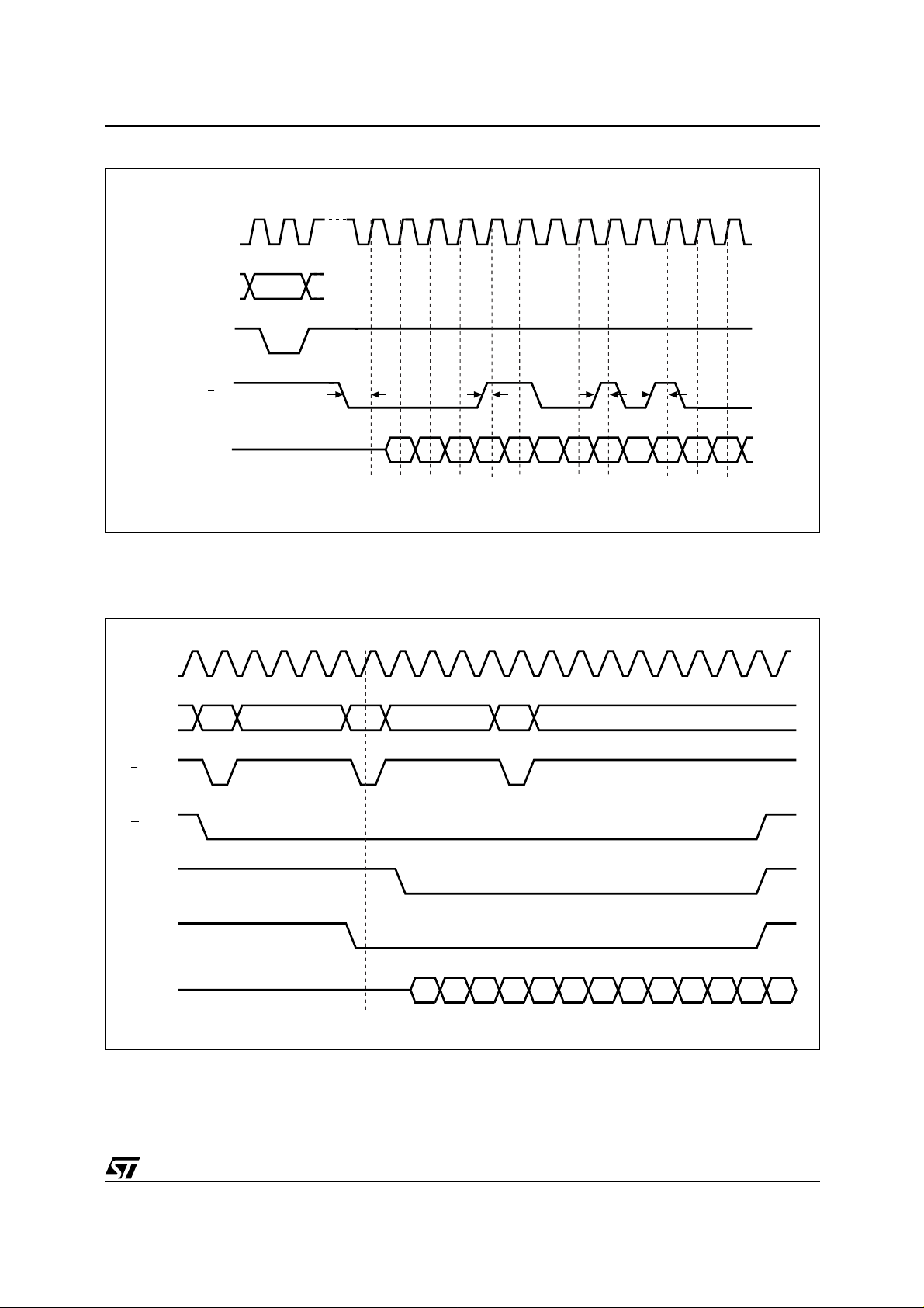
Figure 7. Sync h ronous Burst R ead Operation
M58LV064A, M58LV064B
1
0
K
Address
Inputs
L
B
Data Inputs/
Outputs
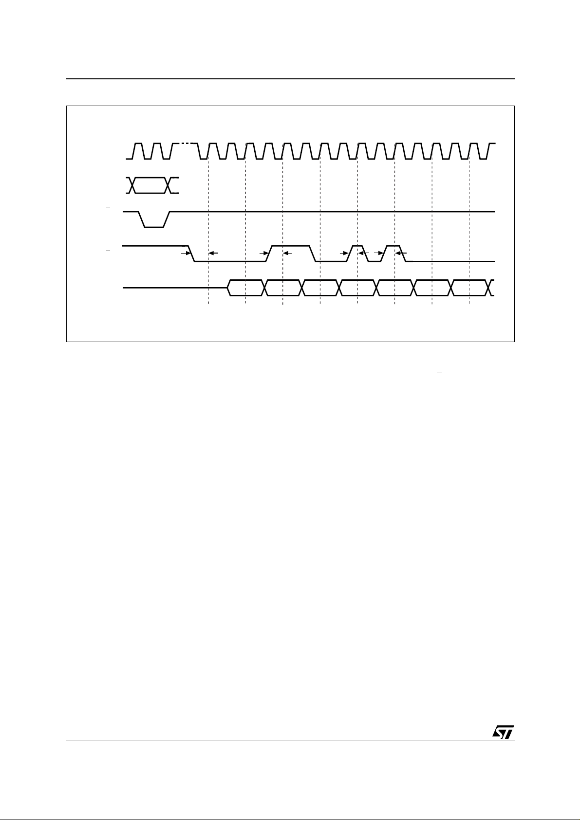
Note: I n thi s exa mple t he Bur st Co nfigur at ion Regist er is set with M 2-M 0 = 001 (B urst Lengt h = 4 Wo rds or Doubl e Word s) , M6 = 1 (Valid
Clock Edge = Rising Clock Edge), M7 = 0 or 1 (Burst Type = Interleaved or Sequential), M9 = 0 (Y-Latency = 1), M14-M11 = 0011 (XLatency = 8) and M15 = 0 (Rea d Se l ect = Synchro nous Burst Read), other bi ts are don’t care.
Q1
X-1
X
tBLKH
Q1
X+1
Q2
tBHKH
tBHKH
Q5Q5Q5Q4Q3 Q7Q6 Q8Q8Q7
tBHKH
AI03454b
Figure 8. Example Sy nchronous Pipelin ed Burst Read Operati on
01234567891011121314
K
15
Address
Inputs
L
E
G
B
Data
Inputs/ Outputs
Note: I n thi s exa mple t he Bur st Co nfigur at ion Regist er is set with M 2-M 0 = 001 (B urst Lengt h = 4 Wo rds or Doubl e Word s) , M6 = 1 (Valid
Clock Edge = Rising Clock Edge), M7 = 0 or 1 (Burst Type = Interleaved or Sequential), M9 = 0 (Y-Latency = 1), M14-M11 = 0011 (XLatency = 8) and M15 = 0 (Rea d Se l ect = Synchro nous Burst Read), other bi ts are don’t care.
Q1 R1 S1
Q1
Q2 Q3 Q4 NV R1 R2 R3 R4 NV S1 S2
NV= Not Valid
S3
AI03455
19/65
M58LV064A, M58LV064B
Figure 9. Example Burst Address Advance and Burst Abort operations
1
0
K
Address
Inputs
L
B
Data Inputs/
Outputs
Note: 1. In this ex amp le the B ur st Co nfigur ati on Reg ister is s et wit h M2- M0 = 01 0 (Bur st Le ngth = 8 Wo rds), M6 = 1 (Val id Cl ock Edg e =
Rising Clock Edge), M 7 = 0 or 1 (B urst Type = In terleaved or Sequenti al ), M9 = 1 (Y-Latency = 2), M14-M1 1 = 0011 (X- Latency =
8) and M15 = 0 (Read Select = Sy nchronous Burst Read), other bits are don’t care.
2. When the system clock f requency is between 33MHz and 50MHz and the Y la tency is set to 2, values of B
cycles, starting from t he first read are not conside red.
Q1
X-2
tBLKH
Q1 Q2
X
X+2
tBHKH
X+6X+4 X+12X+10X+8
tBHKH
Q3 Q4 Q4
tBHKH
Q4Q3
AI03457b
sampled on odd clock
20/65
 Loading...