


64 Mbit (4Mb x 16, Dual Bank, Burst )
FEATURES SUMMARY
■ SUPPLY VOLTAGE
= 1.65V to 2V for Program, Erase and
–V
DD
Read
–V
–V
■ SYNCHRONOUS / ASYNCHRONOUS READ
– Synchronous Burst Read mode : 54MHz
– Asynchronous/ Synchronous Page Read
– Random Access: 85, 90, 100, 120ns
■ PROGRAMMING TIME
– 10µs by Word typical
– Double/Quadruple Word Program option
■ MEMORY BLOCKS
– Dual Bank Memory Array: 16/48 Mbit
– Parameter Blocks (Top or Bott o m location)
■ DUAL OPERATIONS
– Program Erase in one Bank while Read in
– No delay between Read and Write operations
■ BLOCK LOCKING
– All blocks locked at Power up
– Any combination of blocks can be locked
–WP
■ SECURITY
– 128 bit user programmable OTP cells
– 64 bit unique device number
– One parameter block permanently lockable
■ COMMON FLASH INTERFACE (CFI)
■ 100,000 PROGRAM/ERASE CYCLES per
BLOCK
= 1.65V to 3.3V for I/O Buffers
DDQ
= 12V for fast Program (optional)
PP
mode
other
for Block Lock-Down
M58CR064C, M58CR064D
M58CR064P, M58CR064Q
1.8V Supply Flash Memory
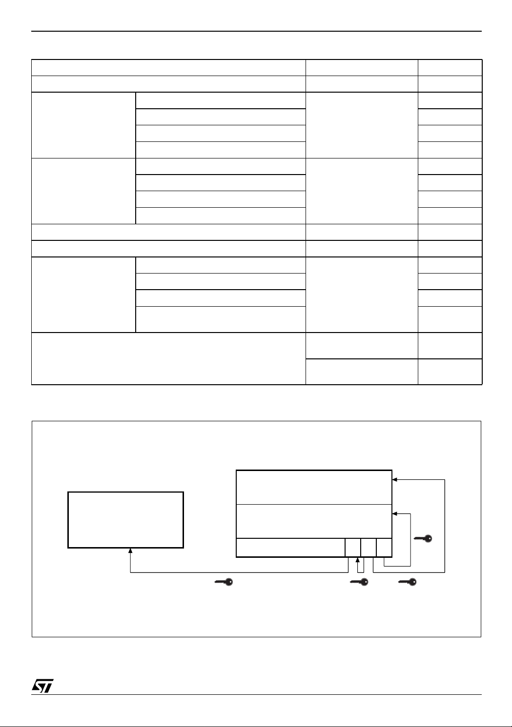
Figure 1. Package
FBGA
TFBGA56 (ZB)
6.5 x 10mm
■ ELECTRONIC SIGNATURE
– Manufacturer Code: 20h
– Top Device Code, M58CR064C: 88CAh
– Bottom Device Code, M58CR064D: 88CBh
– Top Device Code, M58CR064P: 8801h
– Bottom Device Code, M58CR064Q: 8802h
1/70June 2003

M58CR064C, M58CR064D, M58CR064P, M58CR064Q
TABLE OF CONTENTS
SUMMARY DESCRIPTION. . . . . . . . . . . . . . . . . . . . . . . . . . . . . . . . . . . . . . . . . . . . . . . . . . . . . . . . . . . 6
Figure 2. Logic Diagram . . . . . . . . . . . . . . . . . . . . . . . . . . . . . . . . . . . . . . . . . . . . . . . . . . . . . . . . . . 7
Table 1. Signal Names . . . . . . . . . . . . . . . . . . . . . . . . . . . . . . . . . . . . . . . . . . . . . . . . . . . . . . . . . . . 7
Figure 3. TFBGA Connections (Top view through package). . . . . . . . . . . . . . . . . . . . . . . . . . . . . . . 8
Table 2. Bank Architecture . . . . . . . . . . . . . . . . . . . . . . . . . . . . . . . . . . . . . . . . . . . . . . . . . . . . . . . . 8
Figure 4. Memory Map . . . . . . . . . . . . . . . . . . . . . . . . . . . . . . . . . . . . . . . . . . . . . . . . . . . . . . . . . . . 9
SIGNAL DESCRIPTIONS . . . . . . . . . . . . . . . . . . . . . . . . . . . . . . . . . . . . . . . . . . . . . . . . . . . . . . . . . . . 10
Address Inputs (A0-A21). . . . . . . . . . . . . . . . . . . . . . . . . . . . . . . . . . . . . . . . . . . . . . . . . . . . . . . . . 10
Data Input/Output (DQ0-DQ15). . . . . . . . . . . . . . . . . . . . . . . . . . . . . . . . . . . . . . . . . . . . . . . . . . . . 10
Chip Enable (E). . . . . . . . . . . . . . . . . . . . . . . . . . . . . . . . . . . . . . . . . . . . . . . . . . . . . . . . . . . . . . . . 10
Output Enable (G). . . . . . . . . . . . . . . . . . . . . . . . . . . . . . . . . . . . . . . . . . . . . . . . . . . . . . . . . . . . . .10
Write Enable (W). . . . . . . . . . . . . . . . . . . . . . . . . . . . . . . . . . . . . . . . . . . . . . . . . . . . . . . . . . . . . . .10
Write Protect (WP). . . . . . . . . . . . . . . . . . . . . . . . . . . . . . . . . . . . . . . . . . . . . . . . . . . . . . . . . . . . . . 10
Reset/Power-Down (RP). . . . . . . . . . . . . . . . . . . . . . . . . . . . . . . . . . . . . . . . . . . . . . . . . . . . . . . . . 10
Latch Enable (L). . . . . . . . . . . . . . . . . . . . . . . . . . . . . . . . . . . . . . . . . . . . . . . . . . . . . . . . . . . . . . . . 10
Clock (K).. . . . . . . . . . . . . . . . . . . . . . . . . . . . . . . . . . . . . . . . . . . . . . . . . . . . . . . . . . . . . . . . . . . . . 10
Wait (WAIT). . . . . . . . . . . . . . . . . . . . . . . . . . . . . . . . . . . . . . . . . . . . . . . . . . . . . . . . . . . . . . . . . . . 10
Supply Voltage. . . . . . . . . . . . . . . . . . . . . . . . . . . . . . . . . . . . . . . . . . . . . . . . . . . . . . . . . . . . . 10
V
DD
Supply Voltage. . . . . . . . . . . . . . . . . . . . . . . . . . . . . . . . . . . . . . . . . . . . . . . . . . . . . . . . . . . . 10
V
DDQ
V
Program Supply Voltage . . . . . . . . . . . . . . . . . . . . . . . . . . . . . . . . . . . . . . . . . . . . . . . . . . . . .10
PP
V
Ground. . . . . . . . . . . . . . . . . . . . . . . . . . . . . . . . . . . . . . . . . . . . . . . . . . . . . . . . . . . . . . . . . . . 10
SS
Ground. . . . . . . . . . . . . . . . . . . . . . . . . . . . . . . . . . . . . . . . . . . . . . . . . . . . . . . . . . . . . . . . . . 10
V
SSQ
BUS OPERATIONS. . . . . . . . . . . . . . . . . . . . . . . . . . . . . . . . . . . . . . . . . . . . . . . . . . . . . . . . . . . . . . . . 11
Bus Read. . . . . . . . . . . . . . . . . . . . . . . . . . . . . . . . . . . . . . . . . . . . . . . . . . . . . . . . . . . . . . . . . . . . . 11
Bus Write. . . . . . . . . . . . . . . . . . . . . . . . . . . . . . . . . . . . . . . . . . . . . . . . . . . . . . . . . . . . . . . . . . . . . 11
Address Latch.. . . . . . . . . . . . . . . . . . . . . . . . . . . . . . . . . . . . . . . . . . . . . . . . . . . . . . . . . . . . . . . . . 11
Output Disable. . . . . . . . . . . . . . . . . . . . . . . . . . . . . . . . . . . . . . . . . . . . . . . . . . . . . . . . . . . . . . . . . 11
Standby. . . . . . . . . . . . . . . . . . . . . . . . . . . . . . . . . . . . . . . . . . . . . . . . . . . . . . . . . . . . . . . . . . . . . . 11
Reset. . . . . . . . . . . . . . . . . . . . . . . . . . . . . . . . . . . . . . . . . . . . . . . . . . . . . . . . . . . . . . . . . . . . . . . . 11
Table 3. Bus Operations . . . . . . . . . . . . . . . . . . . . . . . . . . . . . . . . . . . . . . . . . . . . . . . . . . . . . . . . . 11
COMMAND INTERFACE . . . . . . . . . . . . . . . . . . . . . . . . . . . . . . . . . . . . . . . . . . . . . . . . . . . . . . . . . . . 12
Table 4. Command Codes. . . . . . . . . . . . . . . . . . . . . . . . . . . . . . . . . . . . . . . . . . . . . . . . . . . . . . . . 12
COMMAND INTERFACE - STANDARD COMMANDS . . . . . . . . . . . . . . . . . . . . . . . . . . . . . . . . . 13
Read Array Command. . . . . . . . . . . . . . . . . . . . . . . . . . . . . . . . . . . . . . . . . . . . . . . . . . . . . . . . . . . 13
Read Status Register Command. . . . . . . . . . . . . . . . . . . . . . . . . . . . . . . . . . . . . . . . . . . . . . . . . . .13
Read Electronic Signature Comma nd . . . . . . . . . . . . . . . . . . . . . . . . . . . . . . . . . . . . . . . . . . . . . . . 13
Read CFI Query Command. . . . . . . . . . . . . . . . . . . . . . . . . . . . . . . . . . . . . . . . . . . . . . . . . . . . . . . 13
Clear Status Register Command. . . . . . . . . . . . . . . . . . . . . . . . . . . . . . . . . . . . . . . . . . . . . . . . . . . 13
Block Erase Command . . . . . . . . . . . . . . . . . . . . . . . . . . . . . . . . . . . . . . . . . . . . . . . . . . . . . . . . . . 13
Program Command. . . . . . . . . . . . . . . . . . . . . . . . . . . . . . . . . . . . . . . . . . . . . . . . . . . . . . . . . . . . . 14
Program/Erase Suspend Comm and . . . . . . . . . . . . . . . . . . . . . . . . . . . . . . . . . . . . . . . . . . . . . . . . 14
2/70

M58CR064C, M58CR064D, M58CR064P, M58CR064Q
Program/Erase Resume Command . . . . . . . . . . . . . . . . . . . . . . . . . . . . . . . . . . . . . . . . . . . . . . . . 14
Protection Register Program Command . . . . . . . . . . . . . . . . . . . . . . . . . . . . . . . . . . . . . . . . . . . . . 15
Set Configuration Register Command. . . . . . . . . . . . . . . . . . . . . . . . . . . . . . . . . . . . . . . . . . . . . . . 15
Block Lock Command . . . . . . . . . . . . . . . . . . . . . . . . . . . . . . . . . . . . . . . . . . . . . . . . . . . . . . . . . . . 15
Block Unlock Command . . . . . . . . . . . . . . . . . . . . . . . . . . . . . . . . . . . . . . . . . . . . . . . . . . . . . . . . . 15
Block Lock-Down Command. . . . . . . . . . . . . . . . . . . . . . . . . . . . . . . . . . . . . . . . . . . . . . . . . . . . . . 15
Table 5. Standard Commands. . . . . . . . . . . . . . . . . . . . . . . . . . . . . . . . . . . . . . . . . . . . . . . . . . . . . 1 6
Table 6. Electronic Signature Codes. . . . . . . . . . . . . . . . . . . . . . . . . . . . . . . . . . . . . . . . . . . . . . . . 17
Figure 5. Security Block and Protection Register Memory Map . . . . . . . . . . . . . . . . . . . . . . . . . . . 17
COMMAND INTERFACE - FACTORY PROGRAM COMMANDS. . . . . . . . . . . . . . . . . . . . . . . . . 18
Bank Erase Command . . . . . . . . . . . . . . . . . . . . . . . . . . . . . . . . . . . . . . . . . . . . . . . . . . . . . . . . . . 1 8
Double Word Program Command . . . . . . . . . . . . . . . . . . . . . . . . . . . . . . . . . . . . . . . . . . . . . . . . . . 18
Quadruple Word Program Command . . . . . . . . . . . . . . . . . . . . . . . . . . . . . . . . . . . . . . . . . . . . . . . 18
Table 7. Factory Program Commands . . . . . . . . . . . . . . . . . . . . . . . . . . . . . . . . . . . . . . . . . . . . . . 19
STATUS REGISTER. . . . . . . . . . . . . . . . . . . . . . . . . . . . . . . . . . . . . . . . . . . . . . . . . . . . . . . . . . . . . . . 20
Program/Erase Controller Status Bit (SR7). . . . . . . . . . . . . . . . . . . . . . . . . . . . . . . . . . . . . . . . . . .20
Erase Suspend Status Bit (SR6) . . . . . . . . . . . . . . . . . . . . . . . . . . . . . . . . . . . . . . . . . . . . . . . . . . . 20
Erase Status Bit (SR5) . . . . . . . . . . . . . . . . . . . . . . . . . . . . . . . . . . . . . . . . . . . . . . . . . . . . . . . . . . 2 0
Program Status Bit (SR4) . . . . . . . . . . . . . . . . . . . . . . . . . . . . . . . . . . . . . . . . . . . . . . . . . . . . . . . . 2 0
V
Status Bit (SR3) . . . . . . . . . . . . . . . . . . . . . . . . . . . . . . . . . . . . . . . . . . . . . . . . . . . . . . . . . . . . 20
PP
Program Suspend Status Bit (SR2). . . . . . . . . . . . . . . . . . . . . . . . . . . . . . . . . . . . . . . . . . . . . . . . .21
Block Protection Status Bit (SR1) . . . . . . . . . . . . . . . . . . . . . . . . . . . . . . . . . . . . . . . . . . . . . . . . . . 2 1
Reserved Bit (SR0) . . . . . . . . . . . . . . . . . . . . . . . . . . . . . . . . . . . . . . . . . . . . . . . . . . . . . . . . . . . . . 21
Table 8. Status Register Bits. . . . . . . . . . . . . . . . . . . . . . . . . . . . . . . . . . . . . . . . . . . . . . . . . . . . . . 2 1
CONFIGURATION REGISTER. . . . . . . . . . . . . . . . . . . . . . . . . . . . . . . . . . . . . . . . . . . . . . . . . . . . . . . 22
Read Select Bit (CR15) . . . . . . . . . . . . . . . . . . . . . . . . . . . . . . . . . . . . . . . . . . . . . . . . . . . . . . . . . . 22
X-Latency Bits (CR13-CR11) . . . . . . . . . . . . . . . . . . . . . . . . . . . . . . . . . . . . . . . . . . . . . . . . . . . . . 22
Power-Down Bit (CR10) . . . . . . . . . . . . . . . . . . . . . . . . . . . . . . . . . . . . . . . . . . . . . . . . . . . . . . . . . 2 2
Wait Configuration Bit (CR8). . . . . . . . . . . . . . . . . . . . . . . . . . . . . . . . . . . . . . . . . . . . . . . . . . . . . . 2 2
Burst Type Bit (CR7). . . . . . . . . . . . . . . . . . . . . . . . . . . . . . . . . . . . . . . . . . . . . . . . . . . . . . . . . . . . 22
Valid Clock Edge Bit (CR6) . . . . . . . . . . . . . . . . . . . . . . . . . . . . . . . . . . . . . . . . . . . . . . . . . . . . . . . 2 2
Wrap Burst Bit (CR3). . . . . . . . . . . . . . . . . . . . . . . . . . . . . . . . . . . . . . . . . . . . . . . . . . . . . . . . . . . . 22
Burst length Bits (CR2-CR0) . . . . . . . . . . . . . . . . . . . . . . . . . . . . . . . . . . . . . . . . . . . . . . . . . . . . . . 23
Table 9. Configuration Register. . . . . . . . . . . . . . . . . . . . . . . . . . . . . . . . . . . . . . . . . . . . . . . . . . . . 23
Table 10. Burst Type Definition. . . . . . . . . . . . . . . . . . . . . . . . . . . . . . . . . . . . . . . . . . . . . . . . . . . . 24
Figure 6. X-Latency and Data Output Configuration Exampl e . . . . . . . . . . . . . . . . . . . . . . . . . . . . 25
Figure 7. Wait Configuration Example. . . . . . . . . . . . . . . . . . . . . . . . . . . . . . . . . . . . . . . . . . . . . . .25
READ MODES. . . . . . . . . . . . . . . . . . . . . . . . . . . . . . . . . . . . . . . . . . . . . . . . . . . . . . . . . . . . . . . . . . . . 26
Asynchronous Read Mode . . . . . . . . . . . . . . . . . . . . . . . . . . . . . . . . . . . . . . . . . . . . . . . . . . . . . . . 26
Synchronous Burst Read Mode. . . . . . . . . . . . . . . . . . . . . . . . . . . . . . . . . . . . . . . . . . . . . . . . . . . . 26
Single Synchronous Read Mode. . . . . . . . . . . . . . . . . . . . . . . . . . . . . . . . . . . . . . . . . . . . . . . . . . .26
3/70

M58CR064C, M58CR064D, M58CR064P, M58CR064Q
DUAL OPERATIONS AND MULTIPLE BANK ARCHITECTURE . . . . . . . . . . . . . . . . . . . . . . . . . . . . 27
Table 11. Dual Operations Allowed In Other Bank . . . . . . . . . . . . . . . . . . . . . . . . . . . . . . . . . . . . . 27
Table 12. Dual Operations Allowed In Same Bank . . . . . . . . . . . . . . . . . . . . . . . . . . . . . . . . . . . . . 27
BLOCK LOCKING. . . . . . . . . . . . . . . . . . . . . . . . . . . . . . . . . . . . . . . . . . . . . . . . . . . . . . . . . . . . . . . . . 28
Reading a Block’s Lock Status . . . . . . . . . . . . . . . . . . . . . . . . . . . . . . . . . . . . . . . . . . . . . . . . . . . . 28
Locked State . . . . . . . . . . . . . . . . . . . . . . . . . . . . . . . . . . . . . . . . . . . . . . . . . . . . . . . . . . . . . . . . . . 28
Unlocked State . . . . . . . . . . . . . . . . . . . . . . . . . . . . . . . . . . . . . . . . . . . . . . . . . . . . . . . . . . . . . . . . 2 8
Lock-Down State. . . . . . . . . . . . . . . . . . . . . . . . . . . . . . . . . . . . . . . . . . . . . . . . . . . . . . . . . . . . . . .28
Locking Operations During Erase Suspend . . . . . . . . . . . . . . . . . . . . . . . . . . . . . . . . . . . . . . . . . . 28
Table 13. Lock Status . . . . . . . . . . . . . . . . . . . . . . . . . . . . . . . . . . . . . . . . . . . . . . . . . . . . . . . . . . . 29
PROGRAM AND ERASE TIMES AND ENDURANCE CYCLES . . . . . . . . . . . . . . . . . . . . . . . . . . . . . 30
Table 14. Program, Erase Times and Program, Erase Endurance Cycles . . . . . . . . . . . . . . . . . . . 30
MAXIMUM RATING. . . . . . . . . . . . . . . . . . . . . . . . . . . . . . . . . . . . . . . . . . . . . . . . . . . . . . . . . . . . . . . . 31
Table 15. Absolute Maximum Ratings. . . . . . . . . . . . . . . . . . . . . . . . . . . . . . . . . . . . . . . . . . . . . . . 31
DC and AC PARAMETERS . . . . . . . . . . . . . . . . . . . . . . . . . . . . . . . . . . . . . . . . . . . . . . . . . . . . . . . . . 3 2
Table 16. Operating and AC Measurement Conditions. . . . . . . . . . . . . . . . . . . . . . . . . . . . . . . . . . 32
Figure 8. AC Measurement I/O Waveform . . . . . . . . . . . . . . . . . . . . . . . . . . . . . . . . . . . . . . . . . . . 32
Figure 9. AC Measurement Load Circuit . . . . . . . . . . . . . . . . . . . . . . . . . . . . . . . . . . . . . . . . . . . . . 32
Table 17. Capacitance. . . . . . . . . . . . . . . . . . . . . . . . . . . . . . . . . . . . . . . . . . . . . . . . . . . . . . . . . . . 32
Table 18. DC Characteristics - Currents . . . . . . . . . . . . . . . . . . . . . . . . . . . . . . . . . . . . . . . . . . . . .33
Table 19. DC Characteristics - Voltages . . . . . . . . . . . . . . . . . . . . . . . . . . . . . . . . . . . . . . . . . . . . .34
Figure 10. Asynchronous Random Access Read AC Waveforms. . . . . . . . . . . . . . . . . . . . . . . . . . 35
Figure 11. Asynchronous Page Read AC Waveforms . . . . . . . . . . . . . . . . . . . . . . . . . . . . . . . . . . 36
Table 20. Asynchronous Read AC Characteristics . . . . . . . . . . . . . . . . . . . . . . . . . . . . . . . . . . . . . 37
Figure 12. Synchronous Burst Read AC Waveforms . . . . . . . . . . . . . . . . . . . . . . . . . . . . . . . . . . . 38
Figure 13. Single Synchronous Read AC Waveforms. . . . . . . . . . . . . . . . . . . . . . . . . . . . . . . . . . . 39
Table 21. Synchronous Read AC Characteristics. . . . . . . . . . . . . . . . . . . . . . . . . . . . . . . . . . . . . . 40
Figure 14. Write AC Waveforms, Write Enable Controlled . . . . . . . . . . . . . . . . . . . . . . . . . . . . . . . 41
Table 22. Write AC Characteristics, Write Enable Controlled . . . . . . . . . . . . . . . . . . . . . . . . . . . . . 42
Figure 15. Write AC Waveforms, Chip Enable Controlled. . . . . . . . . . . . . . . . . . . . . . . . . . . . . . . . 43
Table 23. Write AC Characteristics, Chip Enable Controlled . . . . . . . . . . . . . . . . . . . . . . . . . . . . . 44
Figure 16. Reset and Power-up AC Waveforms . . . . . . . . . . . . . . . . . . . . . . . . . . . . . . . . . . . . . . . 45
Table 24. Reset and Power-up AC Characteristics. . . . . . . . . . . . . . . . . . . . . . . . . . . . . . . . . . . . . 45
PACKAGE MECHANICAL . . . . . . . . . . . . . . . . . . . . . . . . . . . . . . . . . . . . . . . . . . . . . . . . . . . . . . . . . . 46
Figure 17. TFBGA56 6.5x10mm - 8x7 ball array, 0.75 mm pitch, Bottom View Package Outline. . 46
Table 25. TFBGA56 6.5x10mm - 8x7 ball array, 0.75 mm pitch, Package Mechanica l Data . . . . . 46
Figure 18. TFBGA56 Daisy Chain - Package Connections (Top view through package) . . . . . . . . 47
Figure 19. TFBGA56 Daisy Chain - PCB Connection Proposal (Top view through package). . . . . 48
PART NUMBERING . . . . . . . . . . . . . . . . . . . . . . . . . . . . . . . . . . . . . . . . . . . . . . . . . . . . . . . . . . . . . . . 49
Table 26. Ordering Information Scheme . . . . . . . . . . . . . . . . . . . . . . . . . . . . . . . . . . . . . . . . . . . . . 49
4/70

M58CR064C, M58CR064D, M58CR064P, M58CR064Q
Table 27. Daisy Chain Ordering Scheme . . . . . . . . . . . . . . . . . . . . . . . . . . . . . . . . . . . . . . . . . . . . 49
APPENDIX A. BLOCK ADDRESS TABLES . . . . . . . . . . . . . . . . . . . . . . . . . . . . . . . . . . . . . . . . . . . . 50
Table 28. Top Boot Block Addresses, M58CR064C, M58CR064P. . . . . . . . . . . . . . . . . . . . . . . . . 50
Table 29. Bottom Boot Block Addresses, M58CR064D, M58CR064Q . . . . . . . . . . . . . . . . . . . . . . 52
APPENDIX B. COMMON FLASH INTERFACE . . . . . . . . . . . . . . . . . . . . . . . . . . . . . . . . . . . . . . . . . . 54
Table 30. Query Structure Overview. . . . . . . . . . . . . . . . . . . . . . . . . . . . . . . . . . . . . . . . . . . . . . . .54
Table 31. CFI Query Identification String . . . . . . . . . . . . . . . . . . . . . . . . . . . . . . . . . . . . . . . . . . . .54
Table 32. CFI Query System Interface Information. . . . . . . . . . . . . . . . . . . . . . . . . . . . . . . . . . . . . 55
Table 33. Device Geometry Definition. . . . . . . . . . . . . . . . . . . . . . . . . . . . . . . . . . . . . . . . . . . . . . .55
Table 34. Primary Algorithm-Specific Extended Query Table . . . . . . . . . . . . . . . . . . . . . . . . . . . . . 56
Table 35. Burst Read Information . . . . . . . . . . . . . . . . . . . . . . . . . . . . . . . . . . . . . . . . . . . . . . . . . . 57
APPENDIX C. FLOWCHARTS AND PSEUDO CODES. . . . . . . . . . . . . . . . . . . . . . . . . . . . . . . . . . . . 58
Figure 20. Program Flowchart and Pseudo Code . . . . . . . . . . . . . . . . . . . . . . . . . . . . . . . . . . . . . . 58
Figure 21. Double Word Program Flowchart and Pseudo code . . . . . . . . . . . . . . . . . . . . . . . . . . . 59
Figure 22. Quadruple Word Program Flowchart and Pseudo Code . . . . . . . . . . . . . . . . . . . . . . . . 60
Figure 23. Program Suspend & Resume Flowchart and Pseudo Code . . . . . . . . . . . . . . . . . . . . . 61
Figure 24. Block Erase Flowchart and Pseudo Code . . . . . . . . . . . . . . . . . . . . . . . . . . . . . . . . . . . 62
Figure 25. Erase Suspend & Resume Flowchart and Pseudo Code. . . . . . . . . . . . . . . . . . . . . . . . 63
Figure 26. Locking Operations Flowchart and Pseudo Code . . . . . . . . . . . . . . . . . . . . . . . . . . . . . 64
Figure 27. Protection Register Program Flowchart and Pseudo Code . . . . . . . . . . . . . . . . . . . . . . 65
APPENDIX D. COMMAND INTERFACE STATE TABLES . . . . . . . . . . . . . . . . . . . . . . . . . . . . . . . . . 66
Table 36. Command Interface States - Lock table . . . . . . . . . . . . . . . . . . . . . . . . . . . . . . . . . . . . . 66
Table 37. Command Interface States - Modify Table . . . . . . . . . . . . . . . . . . . . . . . . . . . . . . . . . . .67
REVISION HISTORY. . . . . . . . . . . . . . . . . . . . . . . . . . . . . . . . . . . . . . . . . . . . . . . . . . . . . . . . . . . . . . . 68
Table 38. Document Revision History. . . . . . . . . . . . . . . . . . . . . . . . . . . . . . . . . . . . . . . . . . . . . . .68
5/70

M58CR064C, M58CR064D, M58CR064P, M58CR064Q
SUMMARY DESCRIPTION
The M58CR064 is a 64 Mbit (4Mbit x16) non-volatile Flash memory that may be erased electrically
at block level and programmed in-system on a
Word-by-Word basis using a 1.65V to 2V V
ply for the circuitry and a 1.65V to 3.3V V
ply for the Input/Output pins. An optional 12V V
DD
DDQ
sup-
sup-
PP
power supply is provided to speed up customer
programming. In M58CR064C and M58CR064D
the V
pin can also be used as a control pi n to
PP
provide absolute protection against program or
erase. In M58CR064P and M58CR064Q this feature is disabled.
The device features an asymmet rical block architecture. M58CR064 has an array of 13 5 blocks,
and is divided into two banks, Banks A and B. The
Dual Bank Architecture allows Dual Operations,
while programming or erasing in one bank , Read
operations are possible in the other bank. Only
one bank at a time is allowed to be in Program or
Erase mode. It is possible to perform burst reads
that cross bank boundaries. The bank architecture
is summarized in Table 2, and the mem ory maps
are shown in Figure 4. The Parameter Blocks are
located at the top of the memory address space for
the M58CR064C and M58CR064P, and at the bottom for the M58CR064D and M58CR064Q.
Each block can be erased separately. Erase can
be suspended, in order to perform program in any
other block, and then resum ed. Program can be
suspended to read data in any other block and
then resumed. Each block can be programmed
and erased over 100,000 cycles using the supply
voltage V
DD
.
Program and Erase command s are written to the
Command Interface of the memory. An internal
Program/Erase Controller takes care of the timings necessary for program and erase operations.
The end of a program or erase operation can be
detected and any error conditions identified in t he
Status Register. The command set required to
control the memory is consistent with JEDEC standards.
The device supports synchronous burst read and
asynchronous read from all blocks of the memory
array; at power-up the device is configured for
asynchronous read. In synchronous burst mode,
data is output on each clock cycle at frequencies
of up to 54MHz.
The M58CR064 features an instant, individual
block locking scheme that allo ws any block to be
locked or unlocked with no latency, enabling instant code and data protection. All blocks have
three levels of protection. They can be locked and
locked-down individually preventing any accidental programming or erasure. In M58CR064C and
M58CR064D there is an additional hardware protection against program and erase. When V
V
all blocks are protected against program or
PPLK
erase. All blocks ar e loc ke d at Power - Up.
The device includes a Protection Register and a
Security Block to increase the protec tion of a s ys-
tem’s design. The Protection Register is divided
into two segments: a 64 bit segm ent containin g a
unique device number written by ST, and a 128 bit
segment One-Time-Programmable (OTP) by the
user. The user programmable segment can be
permanently protected. The Security Block, parameter block 0, can be permanently protected by
the user. Figure 5, shows the Security Block and
Protection Register Memory Map.
The memory is offered in a TFBGA56, 6.5 x
10mm, 0.75 mm ball pitch package and is supplied
with all the bits erased (set to ’1’).
PP
≤
6/70
M58CR064C, M58CR064D, M58CR064P, M58CR064Q
Figure 2. Logic Diagram Table 1. Signal Names
A0-A21 Address Inputs
A0-A21
W
RP
WP
DQ0-DQ15
V
V
DDQVPP
DD
22
16
DQ0-DQ15
E
WAIT
M58CR064C
G
M58CR064D
M58CR064P
E
G
W
RP
WP
KClock
L
Data Input/Outputs, Command
Inputs
Chip Enable
Output Enable
Write Enable
Reset/Power-Down
Write Protect
Latch Enable
M58CR064Q
WAIT
V
V
V
V
V
DD
DDQ
PP
SS
SSQ
L
K
V
SS
V
SSQ
AI90000
Wait
Supply Voltage
Supply Voltage for Input/Output
Buffers
Optional Supply Voltage for
Fast Program & Erase
Ground
Ground Input/Output Supply
NC Not Connected Internally
7/70
M58CR064C, M58CR064D, M58CR064P, M58CR064Q
Figure 3. TFBGA Connections (Top view through package)
87654321
A
B
C A2
D A1
E
F
G
A13
A15
V
DDQ
V
SS
DQ7 V
A8A11
A9A12
A10
A14 WAIT A16 WP
DQ15
DQ14 DQ11 DQ10 DQ9 DQ0 G
SSQ
V
SS
A20
A21
DQ6
DQ13
DQ5 V
V
DD
K RP
L W
DQ4 DQ2 E A0
DD
V
PP
DQ12
DQ3
A18
DQ1
V
DDQ
A6
A5A17
A7A19
NC
DQ8
V
A4
A3
SSQ
Table 2. Bank Architecture
Bank A 16 Mbit 8 blocks of 4 KWord 31 blocks of 32 KWord
Bank B 48 Mbit - 96 blocks of 32 KWord
8/70
AI90001
Bank Size Parameter Blocks Main Blocks
Figure 4. Me m ory Map
M58CR064C, M58CR064D, M58CR064P, M58CR064Q
Bank B
Bank A
000000h
007FFFh
2F8000h
2FFFFFh
300000h
307FFFh
3F0000h
3F7FFFh
3F8000h
3F8FFFh
3FF000h
3FFFFFh
Top Boot Block
Address lines A21-A0
512 Kbit or
32 KWord
512 Kbit or
32 KWord
512 Kbit or
32 KWord
512 Kbit or
32 KWord
64 Kbit or
4 KWord
64 Kbit or
4 KWord
Total of 96
Main Blocks
(bottom bank)
Total of 31
Main Blocks
(top bank)
Total of 8
Parameter
Blocks
(top bank)
Bank A
Bank B
000000h
000FFFh
007000h
007FFFh
008000h
00FFFFh
0F8000h
0FFFFFh
100000h
107FFFh
3F8000h
3FFFFFh
Bottom Boot Block
Address lines A21-A0
64 Kbit or
4 KWord
Total of 8
Parameter
Blocks
(bottom bank)
64 Kbit or
4 KWord
512 Kbit or
32 KWord
Total of 31
Main Blocks
(bottom bank)
512 Kbit or
32 KWord
512 Kbit or
32 KWord
Total of 96
Main Blocks
(top bank)
512 Kbit or
32 KWord
AI90002
9/70

M58CR064C, M58CR064D, M58CR064P, M58CR064Q
SIGNAL DESCRIPTIONS
See Figure 2 Logic Diagram and Table 1,Signal
Names, for a brief overview of the signals connected to this device.
Address Inputs (A0-A21). The Address Inputs select the cells i n the memory array to a ccess during Bus Read operations. During Bus Write operations they control the commands sent to the Command Interface of the internal state machine.
Data Input/Output (DQ0-DQ15). The Data I/O outputs the data stored at the selected address during a Bus Read operation or inputs a command or the data to be programmed during a Bus Write operation.
Chip Enable (E
). The Chip Enable input acti-
vates the memory control logic, input buffers, decoders and sense amplifiers. When Chip Enable is
and Reset/Power-Down is at VIH the device
at V
IL
is in active mode. When Chip Enable is at V
IH
the
memory is deselected, the outputs are high impedance and the power consumption is reduced to the
stand-b y l e vel .
Output Enable (G
). The Output Enable controls
the outputs during the Bus Read operation of the
memory .
Write Enable (W
). The Write Enable controls the
Bus Write operation of the memory’s Command
Interface. The data and address inputs are latched
on the rising edge of Chip Enable or Write Enable
whichever occurs first.
Write Protect (WP
). Write Protect is an input
that gives an additional hardware protection for
each block. When Write Protect is at V
, the Loc k-
IL
Down is enabled and the prote ction status of t he
Locked-Down blocks cannot be changed. When
Write Protect is at V
, the Lock-Down is disabled
IH
and the Locked-Down blocks can be locked or unlocked. (refer to Table 13, Lock Status).
Reset/Power-Down (RP
). The Reset/Power-
Down input provides a hardware reset of the memory, and/or Power-Down functions, depending on
the Configuration Register status. When Reset/
Power-Down is at V
, the memory is in reset
IL
mode: the outputs are hi gh impedance an d if the
Power-Down function is enabled t he current consumption is reduced to the Reset Supply Current
I
. Refer to Table 18, DC Characte ristics - Cur-
DD2
rents for the value of I
After Reset all blocks
DD2.
are in the Locked state and the Configuration Register is reset. When Reset/Power-Down is at V
IH
the device is in normal operation. Exiting reset
mode the device enters asynchronous read mode,
but a negative transition of Chip Enable or Latch
Enable is required to ensure valid data outputs.
The Reset/Power-Down pin can be interfaced with
3V logic without any additional circuitry. It can be
tied to V
tics).
Latch Enable (L
dress bits on its rising edge. The a ddress latch is
transparent when Latch Enable is at V
hibited when Latch Enable is at V
can be kept Low (also at board level) when the
Latch Enable function is not required or supported.
Clo c k (K). The clock input synchronizes the memory to the microcontroller during synchronous read operations; the address is latched on a Clock edge (rising or falling, according to the configuration settings) when Latch Enable is at V don't care during asynchronous read and in write operations.
Wait (WAIT
synchronous read to indicate whether the dat a on
the output bus are valid. This output is high impedance when Chip Enable or Output Enable are at
V
or Reset/Power-Down is at VIL. It can be con-
IH
figured to be active during the wait cycle or one
clock cycle in advance.
Supply Voltage. VDD provides the power
V
DD
supply to the internal core of the memory device.
It is the main power supply for all operations
(Read, Program and Erase).
Supply Voltage. V
V
DDQ
supply to the I/O pins and enables all Outputs to
be powered independently from V
tied to V
Program Supply Vol t age . VPP is both a
V
PP
control input and a power supply pin. In
M58CR064C/D the two functions are s elected by
the voltage range applied to the pin. In the
M58CR064P/Q the control feature is disabled.
In M58CR064C/D if V
range (0V to V
In this case a voltage lower than V
absolute protection against program or erase,
while V
bles 18 and 19, DC Characteristics for the relevant
values). V
program or erase; a change in its value after the
operation has started does not have any effect and
program or erase operations continue.
If V
is in the rang e of V
PP
supply pin. In this condition V
til the Program/Erase algorithm is completed.
,
V
Ground. VSS ground is the reference for t he
SS
core supply. It must be connected to the system
ground.
Ground. V
V
SSQ
the input/output circuitry driven by V
must be connected to V
(refer to Table 19, DC Characteris-
RPH
). Latch Enable latches the ad-
IL
. Latch Enable
IH
). Wait is an output signal used during
provides the power
DDQ
. V
DD
or can use a separate supply.
DD
is kept in a low voltage
PP
) VPP is seen as a control input.
DDQ
PP
> V
enables these functions (see Ta-
PP1
is only sampled at the beginning of a
PP
it acts as a power
PPH
must be stable un-
PP
ground is the reference for
SSQ
SS
DDQ
PPLK
DDQ
and it is in-
. Clock is
IL
can be
gives an
. V
SSQ
10/70
M58CR064C, M58CR064D, M58CR064P, M58CR064Q
Note: Each device in a system should have
V
DD, VDDQ
and VPP decoupled wi th a 0.1 µF ce-
ramic capacitor close to the pin (high frequency, inherently low inductance capacitors
should be as close as possible to the pack-
BUS OPERATIONS
There are six standard bus operations that control
the device. These are Bus Read , Bus Write, Address Latch, Output Disable, Standby and Reset.
See Table 3, Bus Operations, for a summary.
Typically glitches of less than 5ns on Chip Enable
or Write Enable are ignored by the memory and do
not affect Bus Write operations.
Bus Read. Bus Read operations are used to output the contents of the Memory Array, the Electronic Signature, the Status Register and the Common Flash Interface. Both Chip Enable and Output Enable must be at V
in order to perform a
IL
read operation. The Chip Enable input s hould be
used to enable the device. Out put Enable should
be used to gate data onto the output. The data
read depends on the previous command written to
the memory (see Command Interface section).
Refer to the Read AC Waveform figures and Characteristics tables in the DC and AC Parameters
section for details of when the output becomes valid.
Bus Write. Bus Write operations write Commands to the memory or latch Input Data to be programmed. A bus write operation is initiated when Chip Enable and Write Enable are at V Output Enable at V
. Commands, Input Data and
IH
IL
with
Addresses are latched on the rising edge of Write
Enable or Chip Enable, whichever occurs first. The
addresses can also be latched prior to the write
operation by toggling Latc h Enable. In this case
age). See Figure 9, AC Measurement Load Circuit. The PCB track widths should be sufficient
to carry the re quired V
program and erase
PP
currents.
the Latch Enable shoul d be t ied to V
during the
IH
bus write operation.
See Figures 14 and 15, Write AC Waveforms, and
Tables 22 and 23, Write AC Characteristics, for
details of the timing requirements.
Address Latch. Address latch operations input valid addresses. Both Chip enable and Latch Enable must be at V
during address latch opera-
IL
tions. The addresses are latched on the rising
edge of Latch Enable.
Output Disa bl e . The outputs are high impedance when the Output Enable is at V
.
IH
Standby. Standby di sables most of the internal circuitry allowing a substantial reduction of the current consumption. The memory is in stand-by when Chip Enable and Reset/Power-Down a re at
. The power consumption is reduced to the
V
IH
stand-by level and the ou tputs are se t to high impedance, independently from the Output Enable
or Write Enable inputs. If Chip Enable switches to
V
during a program or erase operation, t he de-
IH
vice enters Standby mode when finished. Reset. During Reset mode the memory is dese-
lected and the outputs are high impedance. The
memory is in Reset mode when Reset/PowerDown is at V
. The power consumption is reduced
IL
to the Standby leve l, inde pendent ly from t he Chip
Enable, Output Enable or Write Enable inputs. If
Reset is pulled to V
during a Program or Erase,
SS
this operation is aborted and the mem ory content
is no longer valid.
Table 3. Bus Operations
Operation E G W L RP WAIT DQ15-DQ0
Bus Read
Bus Write
Address Latch
Output Disable
Standby
Reset X X X X
Note: 1. X = Don’t care.
2. L
can be tied to VIH if the valid address has been previo usly latched.
3. Depends on G
V
IL
V
IL
V
IL
V
IL
V
IH
.
V
IL
V
IH
X
V
IH
XXX
V
IH
V
IL V
V
IH
V
IH
(2)
V
IL
(2)
IL
V
IL
X
V
IH
V
IH
V
IH
V
IH
V
IH
V
IL
Hi-Z Data Input
Data Output or Hi-Z
Hi-Z Hi-Z
Hi-Z Hi-Z
Hi-Z Hi-Z
Data Output
(3)
11/70
M58CR064C, M58CR064D, M58CR064P, M58CR064Q
COMMAND INTERFACE
All Bus Write operations t o the me mory are in terpreted by the Command Interface. Commands
consist of one or more sequential Bus Write operations. An internal Program/Erase Controller handles all timings and verifies the correct execution
of the Program and Erase commands. The Program/Erase Controller provides a S tatus Register
whose output may be read at any ti me to monitor
the progress or the result of the operation.
The Command Interface is reset to read mode
when power is first applied, when exiting from Reset or whenever V
is lower than V
DD
LKO
. Command sequences must be followed exactly. Any
invalid combination of commands will reset the device to read mode.
Refer to Table 4, Command Codes and Appendix
D, Tables 36 and 37, Command Interface States Modify and Lock Tables, for a summary of the
Command Interface.
The Command Interface is split into two type s of
commands: Standard commands and Factory
Program commands. The following sections explain in detail how to perform each command.
Table 4. Command C odes
Hex Code Command
01h Block Lock Confirm
03h Set Configuration Register Confirm
10h Alternative Program Setup
20h Block Erase Setup
2Fh Block Lock-Down Confirm
30h Double Word Program Setup
40h Program Setup
50h Clear Status Register
55h Quadruple Word Program Setup
60h
70h Read Status Register
80h Bank Erase Setup
90h Read Electronic Signature
Block Lock Setup, Block Unlock Setup,
Block Lock Down Setup and Set
Configuration Register Setup
98h Read CFI Query
B0h Program/Erase Suspend
C0h Protection Register Program
D0h
FFh Read Array
Program/Erase Resume, Block Erase
Confirm, Bank Erase Confirm, Block
Unlock Confirm
12/70

M58CR064C, M58CR064D, M58CR064P, M58CR064Q
COMMAND INTERFACE - STANDARD COMMANDS
The following commands are the basic commands
used to read, write to and configure the device.
Refer to Table 5, Standard Commands, in conjunction with the following text descriptions.
Read Array Command
The Read Array comm and returns the addressed
bank to Read Array mode. One Bus Write cycle is
required to issue the Read Array command and return the addressed bank to Read Array mode.
Subsequent read operations will read the addressed location and output t he data. A Read Array command can be issued in one bank while
programming or erasing in the other bank. However if a Read Array co mmand is issued to a bank
currently executing a Program or Erase operation
the command will be ignore d.
Read Status Register Command
A Bank’s Status Register indicates when a Program or Erase operation is complete and t he suc cess or failure of operation itself. Issue a Read
Status Register command to read the Status Register content of the addressed Bank. The Read
Status Register comma nd can be issued at any
time, even during Program or Erase operations.
The following Bus Read operations output the content of the Status Register of the addressed bank.
The Status Register is latched on the falling edge
or G signals, and can be read until E or G re-
of E
turns to V
date the latched data. See Table 8 for the
description of the Status Register Bit s. This m ode
supports asynchronous or single synchronous
reads only.
Read Electronic Signature Command
The Read Electronic Signature command reads
the Manufacturer and Device Codes, the Block
Locking Status, the Protection Register, and the
Configuration Register.
The Read Electronic Signature command consists
of one write cycle to an address within the bot tom
bank. A subsequent read operation in the address
of the bottom bank will output the Manufacturer
Code, the Device Code, the protection Status of
Blocks of the bottom bank, the Die Revision Code,
the Protection Register, or the Read Configuration
Register (see Table 6).
If the first write cycle of Read Electronic Signature
command is issued t o an address within the top
bank, a subsequent read operat ion in an address
of the top bank will output the protection Statu s of
blocks of the top bank. The status of the other
bank is not affected by the command (see Tab le
11). This mode supports asynchronous or sing le
synchronous reads only, it do es not support page
mode or synchronous burst reads.
. Either E or G must be toggled to up-
IH
Read CFI Query Command
The Read CFI Query command is used to read
data from the Common Flash Interface (CFI)
memory area located in the bottom bank. The
Read CFI Query Command consists of one Bus
Write cycle, to an address within the bottom bank.
Once the command is issued subsequent Bus
Read operations in the s ame bank read from the
Common Flash Interface.
If a Read CFI Query command is issued in a bank
that is executing a Program or Erase operation the
bank will go into Read Status Register mode, subsequent Bus Read cycles will output the Status
Register and the Program/Erase controller will
continue to Program or Erase in t he background.
When the Program or Erase operation has finished the device will enter Read CFI Query mode.
This mode supports asynchronous or single synchronous reads only, it does not support page
mode or synchronous burst reads.
The status of the other banks is not affected by the
command (see Table 11). After issuing a Read
CFI Query command, a Read Array command
should be issued to t he address ed bank to return
the bank to read mode.
See Appendix B, Common Flash Interface, Tables
30, 31, 32, 33, 34 and 35 for details on the in formation contained in the Co mmon Flash Interface
memory area.
Clear Status Register Command
The Clear Status Register comm and c an b e us ed
to reset (set to ‘0’) error bits SR1, SR3, SR4 and
SR5 in the Status Register of the addressed bank.
One bus write cycle is required to issue the Clear
Status Register command. After the Clear S tatus
Register command the bank returns to Read Array
mode.
The error bits in the Status Regi ster do not automatically return to ‘0’ when a new command is issued. The error bits i n the Stat us Register should
be cleared before attempting a new Program or
Erase command.
Block Erase Command
The Block Erase com mand can be used to erase
a block. It sets all the bits within the selected block
to ’1’. All previous d ata in th e block is lost. If th e
block is protected then the Erase operation will
abort, the data in the block will not be changed and
the Status Register will output the error. The Block
Erase command can be issued at any moment, regardless of whether the block has been programmed or not.
Two Bus Write cycles are required to issue the
command.
■ The first bus cycle sets up the Erase command.
13/70

M58CR064C, M58CR064D, M58CR064P, M58CR064Q
■ The second latches the block address in the
internal state machine and starts the Program/
Erase Controller.
If the second bus cycle is not Write Erase Confirm
(D0h), Status Register bits SR 4 and SR5 are set
and the command aborts. Erase aborts if Reset
turns to V
. As data integrity cannot be guaran-
IL
teed when the Erase operation is aborted, the
block must be erased again.
Once the command is issued the device outputs
the Status Register data when any address within
the bank is read. At the end o f the operation the
bank will remain in Read Status Register mode until a Read A rray, Read CFI Query o r Read Electronic Signature command is issued.
During Erase operations the bank containing the
block being erased will onl y ac cept the Read Status Register and the Program/Erase Suspend
command, all other commands will be ignored.
Refer to Dual Operations section for detailed information about simultaneous operations allowed in
banks not being erased. Typical Erase times are
given in Table 14, Program, Erase Times and Program/Erase Endurance Cycles.
See Appendix C, Figure 24, Block Erase Flowchart and Pseudo Code, for a suggested flowchart
for using the Block Erase command.
Program Command
The memory array can be programmed word-byword. Only one Word in one bank can be programmed at any one time. Two bus write cycles
are required to issue the Program Command.
■ The first bus cycle sets up the Program
command.
■ The second latches the Address and the Data to
be written and starts the Program/Erase
Controller.
After programming has started, read operations in
the bank being programmed output the Status
Register content.
During Program operations the bank being programmed will only accept the Read Statu s Register and the Program/Erase Suspend command.
Refer to Dual Operations section for detailed information about simultaneous operations allowed in
banks not being programmed. Typical Program
times are given in Table 14, Program, Erase
Times and Program/Erase Endurance Cycles.
Programming aborts if Reset goe s to V
. As data
IL
integrity cannot be guaranteed when the program
operation is aborted, the memory location must be
reprogrammed.
See Appendix C, Figure 20, Program Flowchart
and Pseudo Code, for the f lowchart for using the
Program command.
Program/Erase Suspend Command
The Program/Erase Suspend command is used to
pause a Program or Block Erase operation. A
Bank Erase operation cannot be suspended.
One bus write cycle is required to issue t he Program/Erase Suspend command. Once the Program/Erase Controller has paused bits SR7 , SR6
and/ or SR2 of the Status Register will be set to ‘1’.
The command must be addressed to the bank
containing the Program or Erase operation.
During Program/Erase Suspend the Command Interface will accept the Program/Erase Resume,
Read Array (cannot read the suspended block),
Read Status Register, Read Electronic S ignature
and Read CFI Q uery commands. Additionally, if
the suspend operation was Erase then the Clear
status Register, Program, Block Lock, Block LockDown or Protection Program commands wi ll also
be accepted. The block being erased may be protected by issuing the Block Lock, Block LockDown or Protection Register Program commands.
Only the blocks not being e rased m ay be read or
programmed correctly. When the Program /Erase
Resume command is issued the operation will
complete. Refer to the Dual Operations section for
detailed information about simultaneous operations allowed during Program/Erase Suspend.
During a Program/Erase Suspend, the device can
be placed in standby mode by taking Chip Enable
. Program/Erase is aborted if Reset turns to
to V
IH
V
.
IL
See Appendix C, Figure 23 , Program Suspend &
Resume Flowchart and Pseudo Code, and Figure
25, Erase Suspend & Resume Flowchart and
Pseudo Code for flowcharts for using the Program/
Erase Suspend command.
Program/Erase Resu me Command
The Program/Erase Resume command can be
used to restart the Program/Erase Controller after
a Program/Erase Suspen d command has paused
it. One Bus Write cycle is required to issue the
command. The comm and must be written to the
bank containing the Program or Erase Suspend.
The Program/Erase Resume command changes
the read mode of th e target bank to Read S tatus
Register mode.
If a Program command is iss ued during a Block
Erase Suspend, then the erase cannot be resumed until the programming operation has completed. It is possible to accumulate suspend
operations. For example: su spend an erase operation, start a programming operation, suspend the
programming operation then read the array. See
Appendix C, Figure 23, Program Su spend & Resume Flowchart and Pseudo Code, and Figure 25,
Erase Suspend & Resume Flowchart and Pseudo
14/70

M58CR064C, M58CR064D, M58CR064P, M58CR064Q
Code for flowcharts for using the Program/Erase
Resume command.
Protection Regi ster Pr ogram Com m and
The Protection Register Program command is
used to Program the 128 bit user O ne-Time-Programmable (OTP) segment of the Protection Register. The segment is programmed 16 bits at a
time. When shipped all bits in the segment are set
to ‘1’. The user can only program the bits to ‘0’.
Two write cycles are required to issue the Protec-
tion Register Program command.
■ The first bus cycle sets up the Protection
Register Program command.
■ The second latches the Address and the Data to
be written to the Protection Register and starts
the Program/Erase Controller.
Read operations output the Status Register content after the programming has started.
The segment can be protected by programming bit
1 of the Protection Lock Register. Bit 1 of the Protection Lock Register also protects bit 2 of the Protection Lock Register. Programming bit 2 of the
Protection Lock Register will result in a permanent
protection of Parameter Block #0 (see Figure 5,
Security Block and Protection Register Memory
Map). Attempting to program a previously protected Protection Register will result in a Status Register error. The protection of the Protection
Register and/or the Security Block is not reversible.
The Protection Register Program cannot be suspended. See Appendix C, Figure 27, Protection
Register Program Flowchart and Pseudo Code,
for a flowchart for using the Protection Register
Program command.
Set Conf ig uration Regi s te r C om m and.
The Set Configuration Register command is used
to write a new value to the Configuration Control
Register which defines the burst length, type, X latency, Synchronous/Asynchronous Read mode
and the valid Clock edge configuration.
Two Bus Writ e cycles a re required to i ssue the Set
Configuration Register command.
■ The first cycle writes the setup command and
the address corresponding to the Configuration
Register content.
■ The second cycle writes the Configuration
Register data and the confirm command.
Once the comman d is issued the memory ret urns
to Read mode.
The value for the Configuration Register is always
presented on A0-A15. CR0 is on A0, CR1 on A1,
etc.; the other address bits are ignored.
Block Lock Command
The Block Lock command is used to lock a block
and prevent Program or Erase operations from
changing the data in it. All blocks are locked at
power-up or reset.
Two Bus Write cycles are required to issue the
Block Lock command.
■ The first bus cycle sets up the Block Lock
command.
■ The second Bus Write cycle latc hes the block
address.
The lock status can be monitored for each block
using the Read Electronic Signature command.
Table. 13 shows the Lock Status after issuing a
Block Lock command.
The Block Lock bits are vo latile, once set they remain set until a hardware reset or power-down/
power-up. They are cleared by a Block Unlock
command. Refer to the section, Block Locking, for
a detailed explanation. See Appendix C, Figure
26, Locking Operations Flowchart and Pseudo
Code, for a flowchart for using the Lock command.
Block Unlock Command
The Block Unlock command is used to unlock a
block, allowing the block to be programmed or
erased. Two Bus Write cycles are requ ired to issue the Block Unlock command.
■ The first bus cycle sets up the Block Unlock
command.
■ The second Bus Write cycle latc hes the block
address.
The lock status can be monitored for each block
using the Read Electronic Signature command.
Table 13 shows the protection status after issuing
a Block Unlock command. Refer to the section,
Block Locking, for a detailed expla nation and A ppendix C, Figure 26, Locking Operations Flowchart and Pseudo Code, f or a flowchart for using
the Unlock command.
Block Lock-Down Command
A locked or unlocked block can be locked-down by
issuing the Block Lock-Down command. A lockeddown block cannot be programm ed or erased, or
have its protection status changed when WP
low, V
. When WP is high, V
IL
the Lock-Down
IH,
is
function is disabled and the locked blocks can be
individually unlocked by the Block Unlock command.
Two Bus Write cycles are required to issue the
Block Lock-Down command.
■ The first bus cycle sets up the Block Lock
command.
■ The second Bus Write cycle latc hes the block
address.
15/70
M58CR064C, M58CR064D, M58CR064P, M58CR064Q
The lock status can be monitored for each block
using the Read Electronic Signature command.
Locked-Down blocks revert to the locked (and not
locked-down) state when the device is reset on
power-down. Table. 13 shows the Lo ck Statu s af-
ter issuing a Block Lock-Down command. Refer to
the section, Block Locking, for a detailed explanation and Appendix C, Fi gure 26, Locking Operations Flowchart and Pseudo Code, for a flowchart
for using the Lock-Down command.
Table 5. Standard Commands
Bus Operations
Commands
Cycles
Read Array 1+ Write BKA FFh
Read Status Regist er 1+ Write BKA 70h Read
Read Electronic Signature 1+ Write
Read CFI Query 1+ Write BBKA 98h Read
Clear Status Register 1 Write BKA 50h
Block Erase 2 Write B KA 20h Write BA D0h
Program 2 Write BKA 40h or 10h Write WA PD
Program/E rase Su s pen d 1 Wr i te BKA B0h
Program/Erase Resume 1 Write BKA D0h
Protection Register Program 2 Write PRA C0h Write
Set Configuration Register 2 Write CRD 60h Write
Block Lock 2 Write BKA 60h Write
Block Unlock 2 Write BKA 60h Write
Block Lock-Down 2 Write BKA 60h Write
Note: 1. X = Don’t Care, WA=Word Address in targeted bank, RD=Read Data, SRD=Status Register Data, ESD=Electronic Signature Data,
QD=Query Data, BA=Block Address, BKA= Bank Address, BBKA= Bottom Bank Address, PD=Program Data, PRA=Protection
Register Address, PRD=Protection Register Data, CRD=Configuration Register Data.
2. Must be same bank as in the first cycle. The signature address es are listed i n T able 6.
3. When addre ss ed to a block i n th e T op Bank, re ads Block Prot ection data only.
Op. Add Data Op. Add Data
1st Cycle 2nd Cycle
BBKA or
(3)
BKA
Read
90h Read
WA RD
(2)
BKA
BBKA or
(2,3)
BKA
(2)
BBKA
PRA PRD
CRD
BA 01h
BA D0h
BA
SRD
ESD
QD
03h
2Fh
(3)
16/70
M58CR064C, M58CR064D, M58CR064P, M58CR064Q
Table 6. Electronic Signature Codes
Code Address (h) Data (h)
Manufacturer Code Bottom Bank Address + 00 0020
Top (M58CR064C)
88CA
Bottom (M58CR064D) 88CB
Device Code
Bottom Bank Address + 01
Top (M58CR064P) 8801
Bottom (M58CR064Q) 8802
Lock
0001
Unlocked 0000
Block Protection
Block Address + 02
Locked and Locked-Down 0003
Unlocked and Locked-Down 0002
Reserved Bottom Bank Address + 03 Reserved
Configuration Register Bottom Bank Address + 05 CR
ST Factory Default
xx06
Security Block Permanently Locked xx02
Protection Register Lock
OTP Area Permanently Locked xx04
Security Block and OTP Area Permanently
Locked
Bottom Bank Address + 80
Bottom Bank Address + 81
Bottom Bank Address + 84
xx00
Unique Device
Number
Protection Register
Bottom Bank Address + 85
Bottom Bank Address + 8C
Note: CR=Conf ig uration Regi ster.
OTP Area
Figure 5. Security Block and Protection Register Memory Map
PROTECTION REGISTER
8Ch
SECURITY BLOCK
85h
84h
Parameter Block # 0
81h
80h
User Programmable OTP
Unique device number
Protection Register Lock 2 1 0
AI06181
17/70

M58CR064C, M58CR064D, M58CR064P, M58CR064Q
COMMAND INTERFACE - FACTORY PROGRAM COMMANDS
The Factory Program commands are used to
speed up programming. They require V
V
except for the Bank Eras e command which
PPH
also operates at V
= VDD. Refer to Table 7, Fac-
PP
to be at
PP
tory Program Commands, in conjunction with the
following text descriptions.
Bank Erase Command
The Bank Erase command can be used to erase a
bank. It sets all the bits within the selected bank to
’1’. All previous data in th e ban k is lo st. Th e B ank
Erase command will igno re any protected blocks
within the bank. If all blocks in the ba nk are protected then the Bank Erase operation will abort
and the data in the bank wi ll not b e changed. The
Status Register will not output any error.
Bank Erase operations can be p erformed at both
= V
V
PP
and VPP = VDD.
PPH
Two Bus Write cycles are required to issue the
command.
■ The first bus cycle sets up the Bank Erase
command.
■ The second latches the bank address in the
internal state machine and starts the Program/
Erase Controller.
If the second bus cycle is not Write Bank Erase
Confirm (D0h), Status Register bits SR4 and S R5
are set and the command aborts. Erase aborts if
Reset turns to V
. As data integrity cannot be
IL
guaranteed when the Erase operation is aborted,
the bank must be erased again.
Once the command is issued the device outputs
the Status Register data when any address within
the bank is read. At the end o f the operation the
bank will remain in Read Status Register mode until a Read Array, Read CFI Query or Read Electronic Signature command is issued.
During Bank Erase operations the bank being
erased will only accept the Read Status Regi ster
command, all other commands w ill be ignored . A
Bank Erase operation cannot be suspended.
For optimum performance, Bank Erase commands should be limited to a maximum of 100 Program/Erase cycles per Block. After 100 Program/
Erase cycles the internal algorithm will still operate
properly but some degradation in performance
may occur.
Dual operations are not supported during Bank
Erase operations and the command cannot be
suspended.
Typical Erase times are given in Table 14, Program, Erase Times and Program/Erase Endurance Cycles.
Double Word Program Command
The Double Word Program command improves
the programming throughput by writing a page of
two adjacent words in parallel. The two words
must differ only for the address A0.
Programming should not be attempted when V
is not at V
V
is below V
PP
Three bus write cycles are necessary to issue the
Double Word Program command.
■ The first bus cycle sets up the Double Word
Program Command.
■ The second bus cycle latches the Address and
the Data of the first word to be written.
■ The third bus cycle latches the Address and the
Data of the second word to be written and starts
the Program/Erase Controller.
Read operations in the bank bei ng programmed
output the Status Register content after the programming has started.
During Double Word Program operations the bank
being programmed will only a ccept the Read Status Register command, all other commands will be
ignored. Dual operations are not supported during
Double Word Program operations. It is not recommended to suspend the Double Word Program
command. Typical Program times are given in Table 14, Program, Erase Times and Program/Erase
Endurance Cycles.
Programming aborts if Reset goe s to V
integrity cannot be guaranteed when the program
operation is aborted, the memory locations m ust
be reprogrammed.
See Appendix C, Figure 21, Double Word Program Flowchart and Pseudo Code, for the flowchart for using the Double Word Program
command.
Quadruple Word Program Command
The Quadruple Word Program command improves the programming throughput by writing a
page of four adjacent words in parallel. The four
words must differ only for the addresses A0 and
A1.
Programming should not be attempted when V
is not at V
is below V
V
PP
Five bus write cycles are necessary to issue the
Quadruple Word Program command.
■ The first bus cycle sets up the Double Word
Program Command.
■ The second bus cycle latches the Address and
the Data of the first word to be written.
. The command can be executed if
PPH
PPH
but the result is not guaranteed.
PPH
IL
. The command can be executed if
but the result is not guaranteed.
PPH
PP
. As data
PP
18/70
M58CR064C, M58CR064D, M58CR064P, M58CR064Q
■ The third bus cycle latches the Address and the
Data of the second word to be written.
■ The fourth bus cycle latches the Address and
the Data of the third word to be written.
■ The fifth bus cycl e latches the Addr es s and the
Data of the fourth word to be written and starts
the Program/Erase Controller.
Read operations to the bank being programmed
output the Status Register content after the programming has started.
Programming aborts if Reset goe s to V
. As data
IL
integrity cannot be guaranteed when the program
operation is aborted, the memory locations mu st
be reprogrammed.
During Quadruple Word Program operations the
bank being programmed will only accept the Read
Status Register command, all other commands
will be igno re d.
Dual operations are not supported during Quadruple Word Program operations. It is not recommended to suspend the Quadruple Word Program
command. Typical Program times are given in Table 14, Program, Erase Times and Program/Erase
Endurance Cycles.
See Appendix C, Figure 22, Quadruple Word Program Flowchart and Pseudo Code, for the flowchart for using the Quadruple Word Program
command.
Table 7. Factory Program Commands
Bus Write Operations
Command Phase
Cycles
Bank Eras e 2 BKA 80h BKA D0h
(2)
Double Wor d Program
Quadruple Word
Program
Note: 1. WA=Word A dd ress in t arget ed bank, BKA= Bank A d dress, PD = P r ogram Data, WA1 is t h e S t a rt Addr e s s.
(3)
2. Word Addres ses 1 and 2 must be consecutive Addresses differing only for A0.
3. Word Addres ses 1,2,3 and 4 must be consecutive Addresses di ffering onl y for A0 and A1.
3 BKA 30h WA1 PD1 WA2 PD2
5 BKA 55h WA1 PD1 WA2 PD2 WA3 PD3 WA4 PD4
1st 2nd 3rd 4th 5th
Add Data Add Data Add Data Add Data Add Data
19/70

M58CR064C, M58CR064D, M58CR064P, M58CR064Q
STATUS REGISTER
The M58CR064 has two Status Registers, one for
each bank. The Status Registers provide information on the current or previous Program or Erase
operations executed in each bank. Issue a Read
Status Register command to read the contents of
the Status Register, refer to Read Status Register
Command section for more details. To output the
contents, the Status Register is latched and updated on the falling edge of the Chip Enable or Output
Enable signals, and can be read until Chip Enable
or Ou tpu t Enable return s to V
. The Status Reg-
IH
ister can only be read using single asynchronous
or single synchronous reads. Bus Read operations from any address within the bank, always
read the Status Register during Program and
Erase operations.
The various bits convey information about the status and any errors of the operation. Bits SR7, SR6
and SR2 give information on the status of the bank
and are set and reset by the device. Bits SR5,
SR4, SR3 and SR1 give information on errors,
they are set by the device but must be reset by issuing a Clear Status Register command or a hard-
ware reset. If an error bit is set to ‘1’ the Status
Register should be reset before issuing another
command.
The bits in the Status Register are summarized in
Table 8, Status Register Bits. Refer to Table 8 in
conjunction with the following text descriptions.
Program/Erase Controller Status Bit (SR7). The
Program/Erase Controller Status bit indicates
whether the Program/Erase Controller is act ive or
inactive in the addressed bank. When the Program/Erase Controller Status bit is Low (set to ‘0’),
the Program/Erase Controller is active; when the
bit is High (set to ‘1’), the Prog ram/E rase Cont roller is inactive, and the device is ready to process a
new command.
The Program/Erase Controller Status is Low immediately after a Program/Erase Suspend command is issued until the Program/Erase Controller
pauses. After the Program/Erase Controller pauses the bit is High.
During Program, Erase, o perations the Program/
Erase Controller Status bit can be polled to find the
end of the operation. Other bits in the Status Register should not be tested until the Program/Erase
Controller completes the operation and the bit is
High.
After the Program/Erase Cont roller completes its
operation the Erase Status, Prog ram Status, V
PP
Status and Block Lock Status bits should be tested
for errors.
Erase Suspend Status Bit (SR6). The Erase
Suspend Status bit indicates that an Erase operation has been suspended or is going to be sus-
pended in the addressed block. When the Eras e
Suspend Status bit is High (set to ‘1’), a Program/
Erase Suspend command has been issued and
the memory is waiting for a Program/Erase Resume command.
The Erase Suspend Status should only be considered valid when the Program/Erase Controller Status bit is High (Program/Erase Controller inactive).
SR7 is set within 30µs of the Program/Erase Suspend command being issued therefore the memory may still complete the operation rather than
entering the Suspend mode.
When a Program/Erase Re sume command is issued the Erase Suspend Status bit returns Low.
Erase Status Bit (SR5). The Erase Status bit
can be used to identify if the memory has failed to
verify that the block or bank has erased correctly.
When the Erase Status b it is High (set to ‘1’), the
Program/Erase Controller has applied the maximum number of pulses to the block or bank and
still failed to verify that it has erased correctly. The
Erase Status bit should be read once the Program/
Erase Controller Status bit is High (Program/Erase
Controller inactive).
Once set High, the Erase Status bit can only be reset Low by a Clear Status Register command or a
hardware reset. If set High it should be reset before a new Program or Erase command is issued,
otherwise the new command will appear to fail.
Program Status Bit (SR4). The Program Status
bit is used to identify a Pr ogram failure. When the
Program Status bit is High (set to ‘1’), the Program/Erase Controller has applied the maximum
number of pulses to the byte and still failed to verify that it has programmed correctly. The Program
Status bit should be read once the Program/Erase
Controller Status bit is High (Program/Erase Controller inactive).
Once set High, the Program Status bit can only be
reset Low by a Clear Status Register command or
a hardware reset. If set High it should be reset before a new command is issued, otherwise the new
command will appear to fail.
Status Bit (SR3). The VPP Status bit can be
V
PP
used to identify an invalid v oltage on the V
during Program and Erase operations. The V
pin is only sampled at the beginning of a Program
or Erase operation. Indeterminate results can occur if V
When the V
age on the V
when the V
pin has a voltage that is below the VPP Lockout
Voltage, V
gram and Erase operations cannot be performed.
becomes invalid during an operation.
PP
Status bit is Low (set to ‘0’), the volt-
PP
pin was sampled at a valid voltage;
PP
Status bit is High (set to ‘1’), the V
PP
, the memory is protected and Pro-
PPLK
PP
pin
PP
PP
20/70
M58CR064C, M58CR064D, M58CR064P, M58CR064Q
Once set High, the VPP Status bit can only be reset
Low by a Clear Status Register command or a
hardware reset. If set High it should be reset before a new Program or Erase command is issued,
otherwise the new command will appear to fail.
Program Suspend Status Bit (SR2). The Program Suspend Status bit indicates that a Program
operation has been suspended in the addressed
block. When the Program Suspend Status bit is
High (set to ‘1’), a Program/Erase Suspend command has been issued and the memory is waiting
for a Program/Erase Resume command. The Program Suspend Status should only be considered
valid when the Program/Erase Controller Status
bit is High (Program/Erase Controller inactive).
SR2 is set within 5µs of the Program/Erase Suspend command being issued therefore the memo-
When a Program/Erase Re sume command is issued the Program Suspend Status bit returns Low.
Block Protection Status Bit (SR1). The Block
Protection Status bit can be used to identify if a
Program or Block Erase operation has tried to
modify the contents of a locked block.
When the Block Protection Status bit is High (set
to ‘1’), a Program or Erase operation has been attempted on a locked block.
Once set High, the Block Protection Status bit can
only be reset Low by a Clear Status Register command or a hardware reset. If set High it should be
reset before a new command is issued, otherwise
the new command will appear to fail.
Reserved Bit (SR0). SR0 is reserved. Its value
must be masked.
ry may still complete the operation rather than
entering the Suspend mode.
Table 8. Status Register Bits
Bit Name Type Logic Level Definition
SR7 P/E.C. Status Status
SR6 Erase Suspend Status Status
SR5 Erase Status Error
’1’ Ready
’0’ Busy
’1’ Erase Suspended
’0’ Erase In progress or Completed
’1’ Erase Error
’0’ Erase Success
SR4 Program Status Error
Status
V
SR3
SR2 Program Suspend Status Status
SR1 Block Protection Status Error
SR0 Reserved
Note: Logic level ’1’ is High, ’0’ is Low.
PP
Error
’1’ Program Error
’0’ Program Success
V
’1’
’0’
’1’ Program Suspended
’0’ Program In Progress or Completed
’1’ Program/Erase on protected Block, Abort
’0’ No operation to protected blocks
Invalid, Abort
PP
OK
V
PP
21/70
 Loading...