


32 Mbit (2Mb x 16, Dual Bank, Burst )
FEATURES SUMMARY
■ SUPPLY VOLTAGE
= 1.65V to 2V for Program, Erase and
–V
DD
Read
–V
–V
■ SYNCHRONOUS / ASYNCHRONOUS READ
– Burst mode Read: 54MHz
– Page mode Read (4 Words Page)
– Random Access: 85, 100, 120 ns
■ PROGRAMMING TIME
– 10µs by Word typical
– Double/Quadruple Word programming option
■ MEMORY BLOCKS
– Dual Bank Memory Array: 8/24 Mbit
– Parameter Blocks (Top or Bott o m location)
■ DUAL OPERATIONS
– Read in one Bank while Program or Erase in
– No delay between Read and Write operations
■ BLOCK LOCKING
– All blocks locked at Power up
– Any combination of blocks can be locked
–WP
■ SECURITY
– 64 bit user programmable OTP cells
– 64 bit unique device identifier
– One parameter block permanently lockable
■ COMMON FLASH INTERFACE (CFI)
■ 100,000 PROGRAM/ERASE CYCLES per
BLOCK
= 1.65V to 3.3V for I/O Buffers
DDQ
= 12V for fast Program (optional)
PP
other
for Block Lock-Down
M58CR032C
M58CR032D
1.8V Supply Flash Memory
PRELIMINARY DATA
Figure 1. Packages
FBGA
TFBGA56 (ZB)
6.5 x 10 mm
■ ELECTRONIC SIGNATURE
– Manufacturer Code: 20h
– Top Device Code, M58CR032C: 88C8h
– Bottom Device Code, M58CR032D: 88C9h
September 2002
This is preliminary information on a new product now in development or undergoing evaluation. Details are subject to change without notice.
1/63

M58CR032C, M58CR032D
TABLE OF CONTENTS
SUMMARY DESCRIPTION. . . . . . . . . . . . . . . . . . . . . . . . . . . . . . . . . . . . . . . . . . . . . . . . . . . . . . . . . . . 6
Figure 2. Logic Diagram . . . . . . . . . . . . . . . . . . . . . . . . . . . . . . . . . . . . . . . . . . . . . . . . . . . . . . . . . . 7
Table 1. Signal Names . . . . . . . . . . . . . . . . . . . . . . . . . . . . . . . . . . . . . . . . . . . . . . . . . . . . . . . . . . . 7
Figure 3. TFBGA Connections (Top view through package). . . . . . . . . . . . . . . . . . . . . . . . . . . . . . . 8
Table 2. Bank Architecture . . . . . . . . . . . . . . . . . . . . . . . . . . . . . . . . . . . . . . . . . . . . . . . . . . . . . . . . 8
Figure 4. Memory Map . . . . . . . . . . . . . . . . . . . . . . . . . . . . . . . . . . . . . . . . . . . . . . . . . . . . . . . . . . . 9
Figure 5. Security Block and Protection Register Memory Map . . . . . . . . . . . . . . . . . . . . . . . . . . . . 9
SIGNAL DESCRIPTIONS . . . . . . . . . . . . . . . . . . . . . . . . . . . . . . . . . . . . . . . . . . . . . . . . . . . . . . . . . . . 10
Address Inputs (A0-A20). . . . . . . . . . . . . . . . . . . . . . . . . . . . . . . . . . . . . . . . . . . . . . . . . . . . . . . . . 10
Data Inputs/Outputs (DQ0-DQ15 ). . . . . . . . . . . . . . . . . . . . . . . . . . . . . . . . . . . . . . . . . . . . . . . . . .10
Chip Enable (E). . . . . . . . . . . . . . . . . . . . . . . . . . . . . . . . . . . . . . . . . . . . . . . . . . . . . . . . . . . . . . . . 1 0
Output Enable (G). . . . . . . . . . . . . . . . . . . . . . . . . . . . . . . . . . . . . . . . . . . . . . . . . . . . . . . . . . . . . . 10
Write Enable (W). . . . . . . . . . . . . . . . . . . . . . . . . . . . . . . . . . . . . . . . . . . . . . . . . . . . . . . . . . . . . . . 10
Write Protect (WP). . . . . . . . . . . . . . . . . . . . . . . . . . . . . . . . . . . . . . . . . . . . . . . . . . . . . . . . . . . . . . 10
Reset/Power-Down (RP). . . . . . . . . . . . . . . . . . . . . . . . . . . . . . . . . . . . . . . . . . . . . . . . . . . . . . . . . 10
Latch Enable (L). . . . . . . . . . . . . . . . . . . . . . . . . . . . . . . . . . . . . . . . . . . . . . . . . . . . . . . . . . . . . . . . 10
Clock (K).. . . . . . . . . . . . . . . . . . . . . . . . . . . . . . . . . . . . . . . . . . . . . . . . . . . . . . . . . . . . . . . . . . . . . 10
Wait (WAIT). . . . . . . . . . . . . . . . . . . . . . . . . . . . . . . . . . . . . . . . . . . . . . . . . . . . . . . . . . . . . . . . . . . 10
V
Supply Voltage (1.65V to 2V). . . . . . . . . . . . . . . . . . . . . . . . . . . . . . . . . . . . . . . . . . . . . . . . . . 10
DD
Supply Voltage (1.65V to 3.3V). . . . . . . . . . . . . . . . . . . . . . . . . . . . . . . . . . . . . . . . . . . . . . . 10
V
DDQ
V
Program Supply Voltage (12V). . . . . . . . . . . . . . . . . . . . . . . . . . . . . . . . . . . . . . . . . . . . . . . . .10
PP
V
SS
and V
Grounds. . . . . . . . . . . . . . . . . . . . . . . . . . . . . . . . . . . . . . . . . . . . . . . . . . . . . . . . . . 11
SSQ
BUS OPERATIONS. . . . . . . . . . . . . . . . . . . . . . . . . . . . . . . . . . . . . . . . . . . . . . . . . . . . . . . . . . . . . . . . 12
Asynchronous Read. . . . . . . . . . . . . . . . . . . . . . . . . . . . . . . . . . . . . . . . . . . . . . . . . . . . . . . . . . . . . 12
Asynchronous Page Read. . . . . . . . . . . . . . . . . . . . . . . . . . . . . . . . . . . . . . . . . . . . . . . . . . . . . . . . 12
Asynchronous Write. . . . . . . . . . . . . . . . . . . . . . . . . . . . . . . . . . . . . . . . . . . . . . . . . . . . . . . . . . . . . 12
Output Disable. . . . . . . . . . . . . . . . . . . . . . . . . . . . . . . . . . . . . . . . . . . . . . . . . . . . . . . . . . . . . . . . . 12
Standby. . . . . . . . . . . . . . . . . . . . . . . . . . . . . . . . . . . . . . . . . . . . . . . . . . . . . . . . . . . . . . . . . . . . . . 12
Reset/Power-Down.. . . . . . . . . . . . . . . . . . . . . . . . . . . . . . . . . . . . . . . . . . . . . . . . . . . . . . . . . . . . . 12
Automatic Standby. . . . . . . . . . . . . . . . . . . . . . . . . . . . . . . . . . . . . . . . . . . . . . . . . . . . . . . . . . . . . . 12
Synchronous Single Read . . . . . . . . . . . . . . . . . . . . . . . . . . . . . . . . . . . . . . . . . . . . . . . . . . . . . . . . 1 2
Synchronous Burst Read. . . . . . . . . . . . . . . . . . . . . . . . . . . . . . . . . . . . . . . . . . . . . . . . . . . . . . . . . 1 3
Table 3. Bus Operations . . . . . . . . . . . . . . . . . . . . . . . . . . . . . . . . . . . . . . . . . . . . . . . . . . . . . . . . . 13
Figure 6. Synchronous Single Read Operation. . . . . . . . . . . . . . . . . . . . . . . . . . . . . . . . . . . . . . . . 14
Burst Configuration Register. . . . . . . . . . . . . . . . . . . . . . . . . . . . . . . . . . . . . . . . . . . . . . . . . . . . 15
Read Select Bit (M15) . . . . . . . . . . . . . . . . . . . . . . . . . . . . . . . . . . . . . . . . . . . . . . . . . . . . . . . . . . . 15
X-Latency Bits (M13-M11). . . . . . . . . . . . . . . . . . . . . . . . . . . . . . . . . . . . . . . . . . . . . . . . . . . . . . . . 15
Power-Down Bit (M10). . . . . . . . . . . . . . . . . . . . . . . . . . . . . . . . . . . . . . . . . . . . . . . . . . . . . . . . . . . 15
Wait Bit (M8). . . . . . . . . . . . . . . . . . . . . . . . . . . . . . . . . . . . . . . . . . . . . . . . . . . . . . . . . . . . . . . . . . . 15
Burst Type Bit (M7).. . . . . . . . . . . . . . . . . . . . . . . . . . . . . . . . . . . . . . . . . . . . . . . . . . . . . . . . . . . . . 15
Valid Clock Edge Bit (M6).. . . . . . . . . . . . . . . . . . . . . . . . . . . . . . . . . . . . . . . . . . . . . . . . . . . . . . . . 15
2/63

M58CR032C, M58CR032D
Wrap Burst Bit (M3). . . . . . . . . . . . . . . . . . . . . . . . . . . . . . . . . . . . . . . . . . . . . . . . . . . . . . . . . . . . . 15
Burst length Bits (M2-M0).. . . . . . . . . . . . . . . . . . . . . . . . . . . . . . . . . . . . . . . . . . . . . . . . . . . . . . . . 15
Table 4. Burst Configuration Register. . . . . . . . . . . . . . . . . . . . . . . . . . . . . . . . . . . . . . . . . . . . . . . 16
Table 5. Burst Type Definition . . . . . . . . . . . . . . . . . . . . . . . . . . . . . . . . . . . . . . . . . . . . . . . . . . . . . 17
Figure 7. X-Latency Configuration Sequence . . . . . . . . . . . . . . . . . . . . . . . . . . . . . . . . . . . . . . . . . 18
Figure 8. Wait Configuration Sequence . . . . . . . . . . . . . . . . . . . . . . . . . . . . . . . . . . . . . . . . . . . . . .18
COMMAND INTERFACE . . . . . . . . . . . . . . . . . . . . . . . . . . . . . . . . . . . . . . . . . . . . . . . . . . . . . . . . . . . 19
Read Command. . . . . . . . . . . . . . . . . . . . . . . . . . . . . . . . . . . . . . . . . . . . . . . . . . . . . . . . . . . . . . . . 19
Read Status Register Command. . . . . . . . . . . . . . . . . . . . . . . . . . . . . . . . . . . . . . . . . . . . . . . . . . .19
Read Electronic Signature Comma nd . . . . . . . . . . . . . . . . . . . . . . . . . . . . . . . . . . . . . . . . . . . . . . . 19
Read CFI Query Command. . . . . . . . . . . . . . . . . . . . . . . . . . . . . . . . . . . . . . . . . . . . . . . . . . . . . . . 1 9
Clear Status Register Command . . . . . . . . . . . . . . . . . . . . . . . . . . . . . . . . . . . . . . . . . . . . . . . . . . . 19
Block Erase Command . . . . . . . . . . . . . . . . . . . . . . . . . . . . . . . . . . . . . . . . . . . . . . . . . . . . . . . . . . 19
Bank Erase Command . . . . . . . . . . . . . . . . . . . . . . . . . . . . . . . . . . . . . . . . . . . . . . . . . . . . . . . . . . 20
Program Command. . . . . . . . . . . . . . . . . . . . . . . . . . . . . . . . . . . . . . . . . . . . . . . . . . . . . . . . . . . . . 20
Double Word Program Command . . . . . . . . . . . . . . . . . . . . . . . . . . . . . . . . . . . . . . . . . . . . . . . . . . 20
Quadruple Word Program Command . . . . . . . . . . . . . . . . . . . . . . . . . . . . . . . . . . . . . . . . . . . . . . . 21
Program/Erase Suspend Comm and . . . . . . . . . . . . . . . . . . . . . . . . . . . . . . . . . . . . . . . . . . . . . . . . 21
Program/Erase Resume Command . . . . . . . . . . . . . . . . . . . . . . . . . . . . . . . . . . . . . . . . . . . . . . . . 21
Protection Register Program Command . . . . . . . . . . . . . . . . . . . . . . . . . . . . . . . . . . . . . . . . . . . . . 22
Block Lock Command . . . . . . . . . . . . . . . . . . . . . . . . . . . . . . . . . . . . . . . . . . . . . . . . . . . . . . . . . . . 22
Block Unlock Command . . . . . . . . . . . . . . . . . . . . . . . . . . . . . . . . . . . . . . . . . . . . . . . . . . . . . . . . . 22
Block Lock-Down Command. . . . . . . . . . . . . . . . . . . . . . . . . . . . . . . . . . . . . . . . . . . . . . . . . . . . . . 22
Set Burst Configuration Register Command. . . . . . . . . . . . . . . . . . . . . . . . . . . . . . . . . . . . . . . . . . 22
Table 6. Commands . . . . . . . . . . . . . . . . . . . . . . . . . . . . . . . . . . . . . . . . . . . . . . . . . . . . . . . . . . . . 23
Table 7. Dual Bank Operations . . . . . . . . . . . . . . . . . . . . . . . . . . . . . . . . . . . . . . . . . . . . . . . . . . . . 24
Table 8. Read Electronic Signature. . . . . . . . . . . . . . . . . . . . . . . . . . . . . . . . . . . . . . . . . . . . . . . . . 24
Table 9. Read Block Protection. . . . . . . . . . . . . . . . . . . . . . . . . . . . . . . . . . . . . . . . . . . . . . . . . . . . 24
Table 10. Read Protection Register . . . . . . . . . . . . . . . . . . . . . . . . . . . . . . . . . . . . . . . . . . . . . . . . 25
Table 11. Identifier Codes . . . . . . . . . . . . . . . . . . . . . . . . . . . . . . . . . . . . . . . . . . . . . . . . . . . . . . . . 25
Table 12. Program, Erase Times and Program, Erase Endurance Cycles . . . . . . . . . . . . . . . . . . . 26
BLOCK LOCKING. . . . . . . . . . . . . . . . . . . . . . . . . . . . . . . . . . . . . . . . . . . . . . . . . . . . . . . . . . . . . . . . . 27
Reading a Block’s Lock Status . . . . . . . . . . . . . . . . . . . . . . . . . . . . . . . . . . . . . . . . . . . . . . . . . . . . 27
Locked State . . . . . . . . . . . . . . . . . . . . . . . . . . . . . . . . . . . . . . . . . . . . . . . . . . . . . . . . . . . . . . . . . . 27
Unlocked State . . . . . . . . . . . . . . . . . . . . . . . . . . . . . . . . . . . . . . . . . . . . . . . . . . . . . . . . . . . . . . . . 2 7
Lock-Down State. . . . . . . . . . . . . . . . . . . . . . . . . . . . . . . . . . . . . . . . . . . . . . . . . . . . . . . . . . . . . . . 27
Locking Operations During Erase Suspend . . . . . . . . . . . . . . . . . . . . . . . . . . . . . . . . . . . . . . . . . . 27
Block Lock Status . . . . . . . . . . . . . . . . . . . . . . . . . . . . . . . . . . . . . . . . . . . . . . . . . . . . . . . . . . . . . .28
Lock Status . . . . . . . . . . . . . . . . . . . . . . . . . . . . . . . . . . . . . . . . . . . . . . . . . . . . . . . . . . . . . . . . . . . 28
STATUS REGISTER. . . . . . . . . . . . . . . . . . . . . . . . . . . . . . . . . . . . . . . . . . . . . . . . . . . . . . . . . . . . . . . 29
Program/Erase Controller Status (Bit 7) . . . . . . . . . . . . . . . . . . . . . . . . . . . . . . . . . . . . . . . . . . . . .29
Erase Suspend Status (Bit 6) . . . . . . . . . . . . . . . . . . . . . . . . . . . . . . . . . . . . . . . . . . . . . . . . . . . . . 29
Erase Status (Bit 5). . . . . . . . . . . . . . . . . . . . . . . . . . . . . . . . . . . . . . . . . . . . . . . . . . . . . . . . . . . . . 29
3/63

M58CR032C, M58CR032D
Program Status (Bit 4). . . . . . . . . . . . . . . . . . . . . . . . . . . . . . . . . . . . . . . . . . . . . . . . . . . . . . . . . . . 29
V
Status (Bit 3). . . . . . . . . . . . . . . . . . . . . . . . . . . . . . . . . . . . . . . . . . . . . . . . . . . . . . . . . . . . . . . 29
PP
Program Suspend Status (Bit 2) . . . . . . . . . . . . . . . . . . . . . . . . . . . . . . . . . . . . . . . . . . . . . . . . . . . 29
Block Protection Status (Bit 1). . . . . . . . . . . . . . . . . . . . . . . . . . . . . . . . . . . . . . . . . . . . . . . . . . . . . 30
Reserved (Bit 0). . . . . . . . . . . . . . . . . . . . . . . . . . . . . . . . . . . . . . . . . . . . . . . . . . . . . . . . . . . . . . . . 30
Table 15. Status Register Bits. . . . . . . . . . . . . . . . . . . . . . . . . . . . . . . . . . . . . . . . . . . . . . . . . . . . . 30
MAXIMUM RATING. . . . . . . . . . . . . . . . . . . . . . . . . . . . . . . . . . . . . . . . . . . . . . . . . . . . . . . . . . . . . . . . 31
Table 16. Absolute Maximum Ratings . . . . . . . . . . . . . . . . . . . . . . . . . . . . . . . . . . . . . . . . . . . . . . . 31
DC AND AC PARAMETERS. . . . . . . . . . . . . . . . . . . . . . . . . . . . . . . . . . . . . . . . . . . . . . . . . . . . . . . . . 3 2
Table 17. Operating and AC Measurement Conditions. . . . . . . . . . . . . . . . . . . . . . . . . . . . . . . . . . 32
Figure 9. AC Measurement I/O Waveform . . . . . . . . . . . . . . . . . . . . . . . . . . . . . . . . . . . . . . . . . . .32
Figure 10. AC Measurement Load Circuit. . . . . . . . . . . . . . . . . . . . . . . . . . . . . . . . . . . . . . . . . . . . 32
Table 18. Capacitance. . . . . . . . . . . . . . . . . . . . . . . . . . . . . . . . . . . . . . . . . . . . . . . . . . . . . . . . . . . 32
Table 19. DC Characteristics - Currents . . . . . . . . . . . . . . . . . . . . . . . . . . . . . . . . . . . . . . . . . . . . .33
Table 20. DC Characteristics - Voltages . . . . . . . . . . . . . . . . . . . . . . . . . . . . . . . . . . . . . . . . . . . . .34
Figure 11. Asynchronous Read AC Waveforms . . . . . . . . . . . . . . . . . . . . . . . . . . . . . . . . . . . . . . . 35
Figure 12. Asynchronous Page Read AC Waveforms . . . . . . . . . . . . . . . . . . . . . . . . . . . . . . . . . . 36
Table 21. Asynchronous Read AC Characteristics . . . . . . . . . . . . . . . . . . . . . . . . . . . . . . . . . . . . . 37
Figure 13. Synchronous Burst Read . . . . . . . . . . . . . . . . . . . . . . . . . . . . . . . . . . . . . . . . . . . . . . . .38
Table 22. Synchronous Burst Read AC Characteristics . . . . . . . . . . . . . . . . . . . . . . . . . . . . . . . . . 39
Figure 14. Write AC Waveforms, Write Enable Controlled . . . . . . . . . . . . . . . . . . . . . . . . . . . . . . . 40
Table 23. Write AC Characteristics, Write Enable Controlled . . . . . . . . . . . . . . . . . . . . . . . . . . . . . 41
Figure 15. Write AC Waveforms, Chip Enable Controlled . . . . . . . . . . . . . . . . . . . . . . . . . . . . . . . . 42
Table 24. Write AC Characteristics, Chip Enable Controlled . . . . . . . . . . . . . . . . . . . . . . . . . . . . . 43
Figure 16. Reset and Power-up AC Waveforms . . . . . . . . . . . . . . . . . . . . . . . . . . . . . . . . . . . . . . . 44
Table 25. Reset and Power-up AC Characteristics. . . . . . . . . . . . . . . . . . . . . . . . . . . . . . . . . . . . .44
PACKAGE MECHANICAL . . . . . . . . . . . . . . . . . . . . . . . . . . . . . . . . . . . . . . . . . . . . . . . . . . . . . . . . . . 45
Figure 17. TFBGA56 6.5x10mm - 8x7 ball array, 0.75 mm pitch, Bottom View Package Outline. . 45
Table 26. TFBGA56 6.5x10mm - 8x7 ball array, 0.75 mm pitch, Package Mechani cal Data . . . . . 45
PART NUMBERING . . . . . . . . . . . . . . . . . . . . . . . . . . . . . . . . . . . . . . . . . . . . . . . . . . . . . . . . . . . . . . . 46
Table 27. Ordering Information Scheme . . . . . . . . . . . . . . . . . . . . . . . . . . . . . . . . . . . . . . . . . . . . .46
REVISION HISTORY. . . . . . . . . . . . . . . . . . . . . . . . . . . . . . . . . . . . . . . . . . . . . . . . . . . . . . . . . . . . . . . 47
Table 28. Document Revision History . . . . . . . . . . . . . . . . . . . . . . . . . . . . . . . . . . . . . . . . . . . . . . .47
APPENDIX A. COMMON FLASH INTERFACE . . . . . . . . . . . . . . . . . . . . . . . . . . . . . . . . . . . . . . . . . . 48
Table 29. Query Structure Overview. . . . . . . . . . . . . . . . . . . . . . . . . . . . . . . . . . . . . . . . . . . . . . . .48
Table 30. CFI Query Identification String . . . . . . . . . . . . . . . . . . . . . . . . . . . . . . . . . . . . . . . . . . . .48
Table 31. CFI Query System Interface Information. . . . . . . . . . . . . . . . . . . . . . . . . . . . . . . . . . . . . 49
Table 32. Device Geometry Definition. . . . . . . . . . . . . . . . . . . . . . . . . . . . . . . . . . . . . . . . . . . . . . .49
Table 33. Primary Algorithm-Specific Extended Query Table . . . . . . . . . . . . . . . . . . . . . . . . . . . . . 50
4/63

M58CR032C, M58CR032D
Table 34. Burst Read Information . . . . . . . . . . . . . . . . . . . . . . . . . . . . . . . . . . . . . . . . . . . . . . . . . . 51
Table 35. Security Code Area . . . . . . . . . . . . . . . . . . . . . . . . . . . . . . . . . . . . . . . . . . . . . . . . . . . . . 52
APPENDIX B. FLOWCHARTS AND PSEUDO CODES. . . . . . . . . . . . . . . . . . . . . . . . . . . . . . . . . . . . 53
Figure 18. Program Flowchart and Pseudo Code . . . . . . . . . . . . . . . . . . . . . . . . . . . . . . . . . . . . . . 53
Figure 19. Double Word Program Flowchart and Pseudo code . . . . . . . . . . . . . . . . . . . . . . . . . . . 54
Figure 20. Quadruple Word Program Flowchart and Pseudo Code . . . . . . . . . . . . . . . . . . . . . . . . 55
Figure 21. Program Suspend & Resume Flowchart and Pseudo Code . . . . . . . . . . . . . . . . . . . . . 56
Figure 22. Block Erase Flowchart and Pseudo Code . . . . . . . . . . . . . . . . . . . . . . . . . . . . . . . . . . . 57
Figure 23. Erase Suspend & Resume Flowchart and Pseudo Code. . . . . . . . . . . . . . . . . . . . . . . . 58
Figure 24. Locking Operations Flowchart and Pseudo Code . . . . . . . . . . . . . . . . . . . . . . . . . . . . . 59
Figure 25. Protection Register Program Flowchart and Pseudo Code . . . . . . . . . . . . . . . . . . . . . . 60
APPENDIX C. COMMAND INTERFACE STATE TABLES . . . . . . . . . . . . . . . . . . . . . . . . . . . . . . . . . 61
Table 36. Command Interface States - Lock table . . . . . . . . . . . . . . . . . . . . . . . . . . . . . . . . . . . . . 61
Table 37. Command Interface States - Modify Table . . . . . . . . . . . . . . . . . . . . . . . . . . . . . . . . . . . 62
5/63

M58CR032C, M58CR032D
SUMMARY DESCRIPTION
The M58CR032 is a 32 Mbit (2Mbit x16) non-volatile Flash memory that may be erased electrically
at block level and programmed in-system on a
Word-by-Word basis using a 1.65V to 2 .0V V
supply for the circuitry and a 1.65V to 3.3V V
supply for the Input/Output pins. An opt ional 12V
V
power supply is provided to speed up custom-
PP
er programming. The V
pin can also be used as
PP
a control pin to provide absolute protection against
program or erase.
The device features an asymmet rical block architecture. M58CR032 has an array of 71 blocks and
is divided into two banks , Banks A a nd B, providing Dual Bank operations. While programming or
erasing in Bank A, read operations are possible in
Bank B or vice versa. Onl y one bank at a t ime is
allowed to be in program or erase mode. It is possible to perform burst reads that cross bank
boundaries. The bank architectu re is sum m arized
in Table 2, and the memory maps are show n in
Figure 4. The P ar ame te r Bl o cks are located at th e
top of the memory address space for the
M58CR032C and at the bottom for the
M58CR032D.
Each block can be erased separately. Erase can
be suspended, in order to perform either read or
program in any other block, and then resumed.
Program can be s uspended to read data in any
other block and then resumed. Each block can be
programmed and erased over 100,000 cycles.
Program and Erase command s are written to the
Command Interface of the memory. An on-chip
Program/Erase Controller takes care of the timings necessary for program and erase operations.
The end of a program or erase operation can be
detected and any error conditions identified in the
DD
DDQ
Status Register. The command set required to
control the memory is consistent with JEDEC standards.
The device supports synchronous burst read and
asynchronous read from all blocks of the memory
array; at power-up the device is configured for
page mode read. In synchronous burst mode, data
is output on each clock cycle at frequencies of up
to 54MHz.
The M58CR032 features an instant, individual
block locking scheme that allo ws any block to be
locked or unlocked with no latency, enabling instant code and data protection. All blocks have
three levels of protection. They can be locked and
locked-down individually preventing any accidental programming or erasure. There is an additional
hardware protection against program and erase.
When V
PP
≤ V
all blocks are protected against
PPLK
program or erase. All blocks are locked at Power
Up.
The device includes a 128 b it Protection Register
and a Security Block to increase the protection of
a system’s design. The Prote ction Register is divided into two 64 bit segments. The first segment
contains a unique device numb er writt en by ST,
while the second one is one-time-programmable
by the user. The user programmable segment can
be permanently protected. The Security Block, parameter block 0, can be permanently protected by
the user. Figure 5, shows the Security Block and
Protection Register Memory Map.
The memory is offered in a TFBGA56, 0.75 mm
ball pitch package an d is supplied with all the bi ts
erased (set to ’1’).
6/63
M58CR032C, M58CR032D
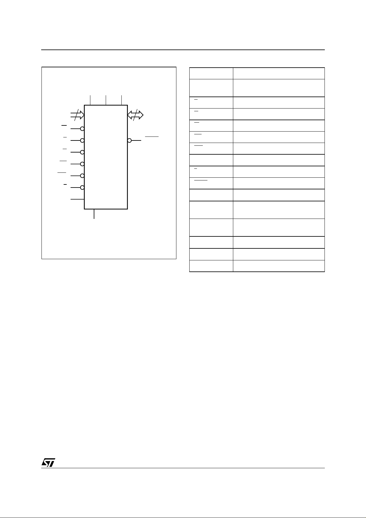
Figure 2. Logic Diagram Table 1. Signal Names
A0-A20 Address Inputs
A0-A20
W
RP
WP
DQ0-DQ15
E
G
21
V
DD
V
DDQVPP
16
DQ0-DQ15
W
E
G
M58CR032C
M58CR032D
WAIT
RP
WP
K Burst Clock
L
L
K
V
SS
AI90067
WAIT
V
DD
V
DDQ
V
PP
V
SS
V
SSQ
Data Input/Outputs or Address
Inputs, Command Inputs
Chip Enable
Output Enable
Write Enable
Reset/Power-down
Write Protect
Latch Enable
Wait Data in Burst Mode
Supply Voltage
Supply Voltage for Input/Output
Buffers
Optional Supply Voltage for
Fast Program & Erase
Ground
Ground Input/Output Supply
NC Not Connected Internally
7/63
M58CR032C, M58CR032D
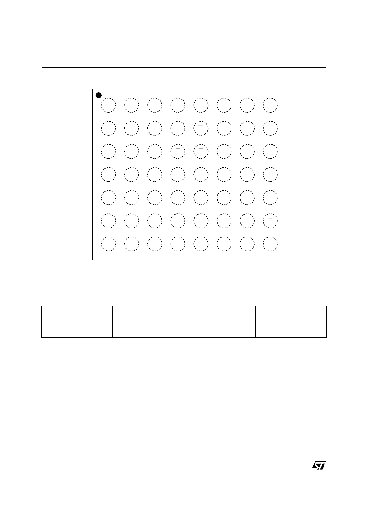
Figure 3. TFBGA Connections (Top view through package)
87654321
A6
A5A17
A7A19
NC
DQ8
V
A4
A3
SSQ
DQ1
V
A18
DDQ
A
B
C A2
D A1
E
F
G
A13
A15
V
DDQ
V
SS
DQ7 V
A8A11
A9A12
A10
A14 WAIT A16 WP
DQ15
DQ14 DQ11 DQ10 DQ9 DQ0 G
SSQ
V
SS
A20
NC
DQ6
DQ13
DQ5 V
V
DD
K RP
L W
DQ4 DQ2 E A0
DD
V
PP
DQ12
DQ3
AI90001
Table 2. Bank Architecture
Bank A 8 Mbit 8 blocks of 4 KWord 15 blocks of 32 KWord
Bank B 24 Mbit - 48 blocks of 32 KWord
8/63
Bank Size Parameter Blocks Main Blocks
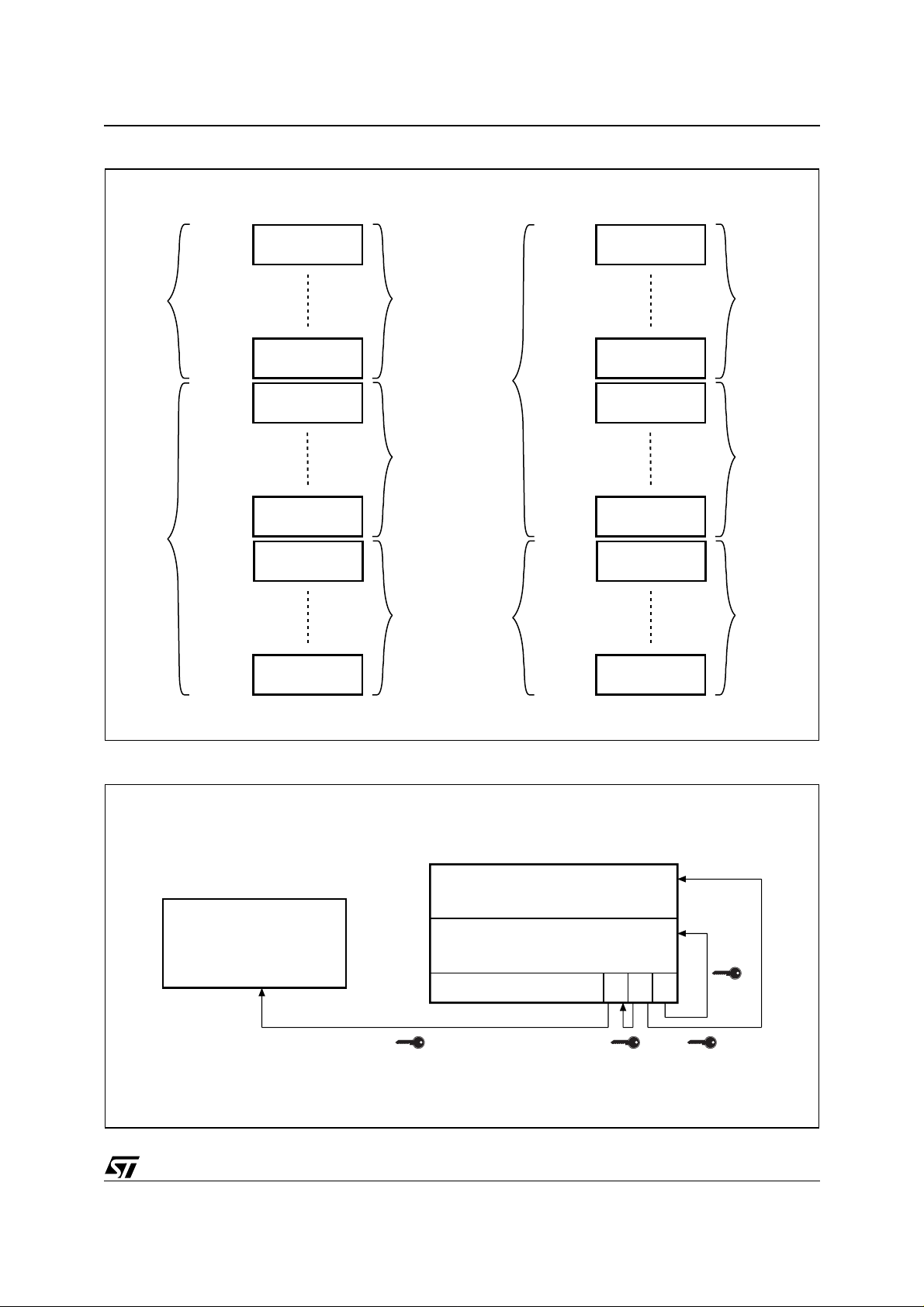
Figure 4. Me m ory Map
M58CR032C, M58CR032D
Bank B
Bank A
000000h
007FFFh
178000h
17FFFFh
180000h
187FFFh
1F0000h
1F7FFFh
1F8000h
1F8FFFh
Top Boot Block
Address lines A20-A0
512 Kbit or
32 KWord
512 Kbit or
32 KWord
512 Kbit or
32 KWord
512 Kbit or
32 KWord
64 Kbit or
4 KWord
Total of 48
Main Blocks
Total of 15
Main Blocks
Total of 8
Parameter
Blocks
Bank A
Bank B
000000h
000FFFh
007000h
007FFFh
008000h
00FFFFh
078000h
07FFFFh
080000h
087FFFh
Bottom Boot Block
Address lines A20-A0
64 Kbit or
4 KWord
Total of 8
Parameter
Blocks
64 Kbit or
4 KWord
512 Kbit or
32 KWord
Total of 15
Main Blocks
512 Kbit or
32 KWord
512 Kbit or
32 KWord
Total of 48
Main Blocks
1FF000h
1FFFFFh
64 Kbit or
4 KWord
1F8000h
1FFFFFh
Figure 5. Security Block and Protection Register Memory Map
PROTECTION REGISTER
SECURITY BLOCK
Parameter Block # 0
88h
85h
84h
81h
80h
User Programmable OTP
Unique device number
Protection Register Lock 2 1 0
512 Kbit or
32 KWord
AI90069
AI90004
9/63

M58CR032C, M58CR032D
SIGNAL DESCRIPTIONS
See Figure 2 Lo gic Diagram, and Tabl e 1, Sign al
Names, for a brief overview of the signals connected to this device.
Address Inputs (A0-A20). The Address Inputs
select the cells i n the memory array to a ccess during Bus Read operations. During Bus Write operations they control the commands sent to the
Command Interface of the internal state machine.
The address inputs for the memory array are
latched on the rising edge of Latch E nable L
address latch is transparent when L
is at VIL. In
synchronous operations the address is also
latched on the first rising/falling edge of K (depending on clock configuration) when L
During a Write operation the address is latched on
the rising edge of L
or W, whichever occurs first.
Data Inputs/Outputs (DQ0-DQ15). The Data Inputs/Outputs output the data stored at the selected
address during a Bus Read operation. During Bus
Write operations they represent the commands
sent to the Command Interface of the internal state
machine.
Both input data and commands are latched on the
rising edge of Write Enable, W
able, E
, and Output Enable, G, are at VIL the data
. When Chip En-
bus outputs data from the Memory Array, the Electronic Signature, Manufacturer or Device codes,
the Block Protection Status, the Burst Configuration Register, the Protection Register or the Status
Register. The data bus is high impedance when
the chip is deselected, Output Enable, G
or Reset/Power-Down, RP
Chip Enable (E
). The Chip Enable input acti-
, is at VIL.
vates the memory control logic, input buffers, decoders and sense amplifiers. When Chi p Enable,
E
, is at VIH, the memory is deselected and the
power consumption is reduced to the standby level. Chip Enable can also be used to control writing
to the Command Interface and to the mem ory array, while Write Enable, W
Output Enable (G
). The Output Enable gates the
, remains at VIL.
outputs through the data buffers during a read operation. When Output Enable, G
, is at VIH the out-
puts are high impedance.
Write Enable (W
). The Write Enable controls the
Bus Write operation of the memory’s Command
Interface. Data are latched on the rising edge of
Write Enable.
Write Protect (WP
). Write Protect is an input that
gives an additional hardware protection for each
block. When Write Protect is at V
, the Lock-Down
IL
is enabled and the protection status of the block
cannot be changed. When Write Protect is at V
the Lock-Down is disabled and the block can be
locked or unlocked. (refer to Table 10, Read Protection Register).
. The
is low.
, is at VIH,
IH
Reset/Power-Down (RP
). The Reset/Power-
Down input provides hardware reset of the memory, and/or Power-Down functions, depending on
the Burst Configuration Register status. A Reset or
Power-Down of the memory is achieved by pulling
RP
to VIL for at least t
. When the reset pulse
PLPH
is given, the memory will recover from PowerDown (when enabled) in a minimum of t
t
or t
PHLL
the rising edge of RP
(see Table 25 and Figure 16) after
PHWL
. After a Reset or Power-Up
the device is configured for asynchronous page
read (M15=1) and the power save func tion is disabled (M10=0). All blocks are locked after a Reset
or Power-Down. Either Chip Enable or W rite Enable must be tied to V
during Power-Up to allow
IH
maximum security and the possibility to write a
command on the first rising edge of Write Enable.
Latch Enable (L
). Latch Enable l atches t he ad-
dress bits A0-A20 on its rising edge. The address latch is transparent when L
it is inhibited when L
is at VIH.
is a t VIL and
Clo c k (K). The clock input synchronizes the
memory to the microcontroller during burst mode
read operation; the address is latched on a K edge
(rising or falling, according to the configuration settings) when L
is at VIL. K is don't care during asyn-
chronous page mode read and in write operations.
Wait (WAIT
). Wait is an output signal used during
burst mode read, indicating whether the data on
the output bus are valid or a wait state must be inserted. This output is high impedance when C hip
Enable or Output Enable are at V
er-Down is at V
. It can be configured to be active
IL
or Reset/Pow-
IH
during the wait cycle or one clock cycle in advance.
Supply Voltage (1.65V to 2V). V
V
DD
vides the power supply to the internal core of the
memory device. It is the main power supply for all
operations (Read, Program and Erase). It ranges
from 1.65V to 2.0V.
Supply Voltage (1.65V to 3.3V). V
V
DDQ
provides the power supply to the I/O pins and enables all Outputs to be powered independently
from V
DD
. V
can be tied to VDD or it can use a
DDQ
separate supply. It can be powered either from
1.65V to 2.0V or from 1.65V to 3.3V.
V
Program Supply Voltage (12V).
PP
is a power supply pin. The Supply Voltage
V
PP
and the Program Supply Voltage VPP can be
V
DD
applied in any order. The pin can also be used as
a control input.
The two functions are selected by the voltage
range applied to the pin. If V
,
age range (0V to 2V) V
is kept in a low volt-
PP
is seen as a control in-
PP
put. In this case a voltage lower than V
an absolute protection against program or era se,
DD
PPLK
DDQ
gives
PHEL
pro-
,
10/63

M58CR032C, M58CR032D
while VPP > V
enables these functions (see Ta-
PP1
ble 19, DC Characteristics for the relevant values).
V
is only sampled at the beginning of a program
PP
or erase; a change in its value after the operation
has started does not have any effect on Program
or Erase, however for Double or Quadruple Word
Program the results are uncertain.
is in the range 11.4V to 12.6V it acts as a
If V
PP
power supply pin. In this condition V
must be
PP
stable until the Program/Erase algorit hm is completed (see Table 16 and 17). In read mode the
current sunk is less then 0.5mA, while during pro-
gram and erase operations the current may increase up to 10mA.
V
and V
SS
Grounds. VSS and V
SSQ
SSQ
grounds
are the reference for the core supply and the input/
output voltage measurements respectively.
Note: Each device in a system should have
V
DD, VDDQ
and VPP decoupled wi th a 0.1 µF ca-
pacitor close to the pin. See Figure 10, AC Measurement Load Circu it. The PCB trace widths
should be sufficient to carry the required V
PP
program and erase currents.
11/63

M58CR032C, M58CR032D
BUS OPERATIONS
There are two types of bus operations that control
the device: Asynchronous (Read, Page Read,
Write, Output Disable, Standby, Automatic Standby and Reset/Power-Down) and Synchronous
(Synchronous Read and Synchronous Burst
Read).
The Dual Bank architecture of the M58CR032 allows read/write operations in Bank A, while read
operations are being executed in Bank B or vice
versa. Write operations are only allowed in one
bank at a time (see Table 7).
See Table 3, Bus Operations, for a summary. Typically glitches of less than 5ns on Chip Enab le or
Write Enable are ignored by the memory and do
not affect bus operations.
Asynchronous Read. Asynchronous Read operations read from the Memory Array, or specific
registers (Electronic Signature, Status Register,
CFI, Block Protection Status, Read Configuration
Register status and Protection Register) in the
Command Interface.
A valid Asynchronous Bus Read operation involves setting the desired address on the Address
Inputs, applying a Low sig nal, V
and Output Enable and keeping Write Enable
High, V
edge of the Latch, L
. The address is latched on the rising
IH
, input. The Data Inputs/Outputs will output the value, see Figure 11, Asynchronous Read AC Waveforms, and Table 21,
Asynchronous Read AC Characteristics, for details of when the output becomes valid.
According to the device configuration the following
Read operations: Electronic Signature, Status
Register, CFI, Block Protection Status, Burst Configuration Register Status and Protection Register
must be accessed as asynchronous read or as
single synchronous read.
Asynchronous Page Read. Asynchronous
Page Read operations can be used to read the
content of the memory array, where data is internally read and stored in a page buffer. The page
has a size of 4 words and is addressed by A0 and
A1 address inputs.
Valid bus operations are the same as Asynchronous Bus Read operations but with different timings. The first read operation within the page has
identical timings, subsequent reads within the
same page have much sh orter access t i mes. If the
page changes then the normal, longer timings apply again. See Figure 12, Asynchronous Page
Read AC Waveforms and Table 21, Asynchronous Read AC Characteristics for details on when
the outputs become valid.
Asynchronous Page Read is the default st ate of
the device when exiting power-down or after power-up.
, to Chip Enable
IL
Asynchronous Write. Bus Write operations are
used to write to the Command Interface of the
memory or latch Input Data to be programmed. A
valid Bus Write operation begins by setting the desired address on the Address Inputs and setting
Chip Enable, E
Output Enable to V
the rising edge of L
, and Write Enable, W, to VIL and
. Addresses are latched on
IH
, W or E whichever occur first.
Commands and Input Data are latched on t he rising edge of W
Enable must remain High, V
or E whichever occurs first. Output
, during the whole
IH
Bus Write operation. See Figures 14 and 15, Write
AC Waveforms, and Tables 23 and 24, Write AC
Characteristics, for details of the timing requirements.
Write operations are asynchronous and the clock
is ignored during write.
Output Disa bl e . The data outputs are high impedance when the Output Enable, G
Enable, W
, are High, VIH.
Standby. When Chip Enable is High, V
, and Write
, and the
IH
Program/Erase Controller is idle, the m emory enters Standby mode and t he Data Inputs/Outputs
pins are placed in the high impedance state, independent of Output Enable, G
, or Write Enable, W.
For the Standby current level see T able 19, DC
Characteristics.
Reset/Power-Down. The memory is in PowerDown when the Burst Configuration Register is set
for Power-Down and RP
is at VIL. The power consumption is reduced to the Power-Down level, and
Outputs are in high impedance, independent of
Chip Enable E
W
. The memory is in reset mode when the Burst
Configuration Register is set for Reset and RP
. The power consumption is the s am e of t he
at V
IL
, Output Enabl e G or Write Ena ble
is
standby and the outputs are in hig h impedance.
After a Reset/Power-Down the de vice defaults to
Asynchronous Page Read, the Status Register is
cleared and the Burst configuration register defaults to Asynchronous Page read.
Automatic Standby. If CMOS levels (V
DD
±
0.2V) are used to drive the b us and the bu s is inactive for 150ns or more in Read mode, the memory enters Automatic Standby where the internal
Supply Current is reduced to the Standby Supply
Current, I
. The Data Inputs/Outputs will still
DD2
output data if a Bus Read operation is in progress.
The automatic standby feature is not available
when the device is configured for synchronous
burst mode.
Synchronous Single Read. Synchronous single Reads can be used to read the Electronic Signature, Status Register, CFI, Block Protection
Status, Burst Configuration Register Status or
12/63
M58CR032C, M58CR032D
Protection Register, see F igure 6, for an example
of a single synchronous read operation.
Synchronous Burst Read. The device also supports a synchronous burst read. In this mode a
burst sequence is started at the f irst clock edge
(rising or falling according to configuration settings) after the falling edge o f La tch Enable. After
a configurable delay of 2 to 5 clock c ycles a new
data is output at e ach clock cycle. The burst sequence may be configured t o be sequent ial or interleaved and for a length of 4 or 8 words or for
continuous burst mode (s ee Table 5, Burst Type
Definition). Wrap and no-wrap modes are also
supported.
A WAIT
system that an output delay will occur. This delay
will depend on the starting address of the burst sequence; the worst case dela y will o ccur w hen the
sequence is crossing a 64 word boundary and the
starting address was at the end of a four word
boundary. See the Burst Configuration Register
command for more details on all the possible settings for the synchronous burst read (see Table 4).
It is possible to perform burst read across bank
boundaries (all banks in read array mode).
Table 3. Bus Operations
Operation E G W L KRPWP DQ15-DQ0
Asynchronous Read
Asynchronous Page Read
Asynchronous Write
Output Disable
Standby
V
IL
V
IL
V
IL
V
IL
V
IH
V
IL
V
IL
V
IH
V
IH
V
IH V
V
IH
V
IL
V
IH
XXXX
Reset / Power-Down X X X X X
Synchronous Read
Synchronous Burst Read
Note: 1. X = Don’t care.
2. T = transition, falling edge for L
is started on the first active clock edge after the falling edge of Latch Enable.
3. L
can be tied to VIH if the valid address has been previously latched
V
IL
V
IL
, rising or falling edge for K depending on M6 in the Burst Configu ration Register. The burst sequence
V
IL
V
IL
V
IH
V
IH
(3)
IL
(3)
V
IL
(3)
V
IL
XX
(2)
T
(2)
T
signal may be asserted to indicate to the
X
X
X
(2)
T
(2)
T
V
IH
V
IH
V
IH
V
IH
V
IH
V
IL
V
IH
V
IH
X Data Output
X Data Output
V
IH
V
IH
Data Input
Hi-Z
X Hi-Z
X Hi-Z
X Data Output
X Data Output
13/63
M58CR032C, M58CR032D
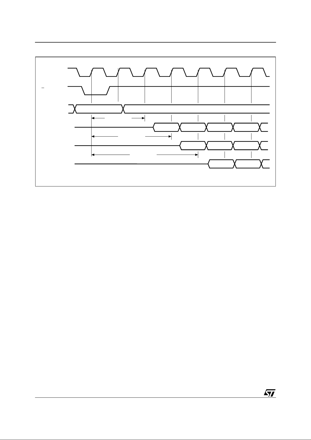
Figure 6. Synchronous Single Read Operation
K
L
A20-A0
DQ15-DQ0
DQ15-DQ0
DQ15-DQ0
VALID ADDRESS
X latency = 2
X latency = 3
X latency = 4
VALID DATA NOT VALID
VALID DATA
NOT VALID
NOT VALID
VALID DATA
NOT VALID
NOT VALID
NOT VALID
AI90103
14/63

M58CR032C, M58CR032D
Burst Configuration Register
The Burst Configuration Register is used to configure the type of bus access that the memory will
perform.
The Burst Configuration Register is set through
the Command Interface. After a Reset or PowerUp the device is configured for asynchronous
page read (M15 = 1) and the power sav e func tion
is disabled (M10 = 0). The Burst Configuration
Register bits are described in Table 4. They specify the selection of the burst length, burst type,
burst X latency and the Read operation. Refer to
Figures 7 and 8 for examples of synchronous burst
configurations.
Read Select Bit (M15). The Read Select bit,
M15, is used to switch between asynchronous and
synchronous Bus Read operations. When the
Read Select bit is set to ’1’, Bus Read operations
are asynchronous; when the Read Select but is
set to ’0’, Bus Read operations are synchronou s.
Synchronous Burst Read is supported in both parameter and main blocks and can be performed
across banks.
On reset or power-up the Read Sel ect bit is set
to’1’ for asynchronous access.
X-Latency Bits (M13-M11). The X-Latency bits
are used during Synchronous Bus Read operations to set the n umber of clock cycl es between
the address being latched and the first data becoming available. For correct operation the X-Latency bits can only assume the values in Table 4,
Burst Configuration Register.
The correspondence be tween X-Latency settings
and the maximum sustainable freq uency must be
calculated taking into account some system parameters.
Two conditions must be satisfied:
–(n + 1) t
–tK > t
KQV
K
+ t
- t
ACC
AVK_CPU
QVK_CPU
+ t
QVK_CPU
≥ t
where "n" is the chosen X-Latency configuration
code, t
is the clock period, t
K
Address Valid, L
last, and t
QVK_CPU
Low or E Low, whichever occurs
AVK_CPU
is the data setup t ime required
is Cloc k to
by the system CPU.
Power-Down Bit (M10). The Power-Down bit is
used to enable or disable the power-down function. When the Power-Down bit is set to ‘0’ (default) the power-down func tion is disabled. W hen
the Power-Down bit is set to ‘1’ power-down is enabled and the device goes into the power-down
state where the I
typical figure of I
supply current is reduced to a
DD
.
DD2
if this function is disabled the Reset/Power-Down,
RP
, pin causes o nly a reset of the dev i ce and the
supply current is the standby value. The recovery
time after a Reset/Power-Down, RP
, pulse is sig-
nificantly longer when power-down is enabled
(see Table 25).
Wait Bit (M8). In burst mode the Wait bit controls
the timing of the Wait output pin, WAIT
. When the
Wait bit is ’0’ the Wait output pin is asserted during
the wait state. When the Wait bit is ’1’ (default) the
Wait output pin is asserted one clock cycle before
the wait state.
WAIT
is asserted during a continuous burst and
also during a 4 or 8 burst length if no-wrap configuration is selected. WAIT
is not asserted during
asynchronous reads, single synchronous reads or
during latency in synchronous reads.
Burst Type Bit ( M7 ). The Burst Type bit is used
to configure the sequence of addresses read as
sequential or interleaved. When the Burst Type bit
is ’0’ the memory outputs from interleaved addresses; when the Burst Type bit is ’1’ (default) the
memory outputs from sequential addresses. See
Tables 5, Burst Type Definition, for the seq uence
of addresses output from a given starting address
in each mode.
Valid Clock Edge Bit (M6). The Valid Clock
Edge bit, M6, is used to configu re the active e dge
of the Clock, K, during Synchronous Burst Read
operations. When the Valid Clock Edge bit is ’0’
the falling edge of the Clock is the active edge;
when the Valid Clock Edge bit is ’1’ the rising edge
of the Clock is active.
Wrap Burst Bit (M3). The burst reads can be
confined inside the 4 or 8 Double-Word boundary
(wrap) or overcome the boundary (no wrap). The
Wrap Burst bit is used to select between wrap and
no wrap. When the Wrap Burst bit is set to ‘0’ the
burst read wraps; when it is set to ‘1’ the burst read
does not wrap.
Burst length Bits (M2-M0). The Burst Length
bits set the number of Words to be output during a
Synchronous Burst Read operation; 4 words, 8
words or continuous burst, where all the words are
read sequentially.
In continuous burst mode the burs t sequ ence c an
cross bank boundaries.
In continuous burst mode or in 4, 8 words no-wrap,
depending on the starting add ress, the dev ice activates the WAIT
output to indicate that a delay is
necessary before the data is output.
If the starting address is aligned to a 4 word
boundary no wait states are needed and the WAIT
output is not activated.
If the starting address is shifted by 1,2 or 3 positions from the four word boundary, WAIT
will b e
asserted for 1, 2 or 3 clock cycles when the burst
sequence crosses the first 64 word b oundary, to
indicate that the device needs an internal delay to
read the successive words in the array. WAIT
will
15/63
M58CR032C, M58CR032D
be asserted only once during a continuous burst
access. See also Table 5, Burst Type Definition.
Table 4. Burst Configuration Registe r
Bit Description Value Description
M15 Read Select
M14 Reserved
M13-M11
M10
M9 Reserved
M8 Wait
X-Latency
Power-Down
(2)
(3)
0 Synchronous Burst Read
1 Asynchronous Page Read (Default at power-on)
010 2 clock latency
011 3 clock latency
100 4 clock latency
101 5 clock latency
111 Reserved
Other configurations reserved
0 Power-Down disabled
1 Power-Down enabled
0 WAIT
1 WAIT
M14, M9 , M5 and M4 are reserved for future use.
is active during wait state
is active one data cycle before wait state (default)
M7 Burst Type
M6 Valid Clock Edge
M5-M4 Reserved
M3 Wrapping
M2-M0 Burst Length
0 Interleaved
1 Sequential (default)
0 Falling Burst Clock edge
1 Rising Burst Clock edge
0 Wrap
1 No wrap
001 4 words
010 8 words
111 Continuous (M7 must be set to ‘1’)
16/63
Tabl e 5. Burst Type Definition
Start
Address 4 Words 8 Words
Mode
Sequential Interleaved Sequential Interleaved
0 0-1-2-3 0-1-2-3 0-1-2-3-4-5-6-7 0-1-2-3-4-5-6-7 0-1-2-3-4-5-6...
1 1-2-3-0 1-0-3-2 1-2-3-4-5-6-7-0 1-0-3-2-5-4-7-6 1-2-3-4-5-6-7...
2 2-3-0-1 2-3-0-1 2-3-4-5-6-7-0-1 2-3-0-1-6-7-4-5 2-3-4-5-6-7-8...
3 3-0-1-2 3-2-1-0 3-4-5-6-7-0-1-2 3-2-1-0-7-6-5-4 3-4-5-6-7-8-9...
...
7 7-4-5-6 7-6-5-4 7-0-1-2-3-4-5-6 7-6-5-4-3-2-1-0 7-8-9-10-11-12-13...
Wrap
...
60 60-61-62-63-64-65-66...
61 61-62-63-WAIT-64-65-66...
62 62-63-WAIT-WAIT-64-65-66...
63
Sequential Interleaved Sequential Interleaved
0 0-1-2-3 0-1-2-3-4-5-6-7 0-1-2-3-4-5-6...
M58CR032C, M58CR032D
Continuous Burst
63-WAIT-WAIT-WAIT-64-65-
66...
1 1-2-3-4 1-2-3-4-5-6-7-8 1-2-3-4-5-6-7...
2 2-3-4-5 2-3-4-5-6-7-8-9... 2-3-4-5-6-7-8...
3 3-4-5-6 3-4-5-6-7-8-9-10 3-4-5-6-7-8-9...
...
7 7-8-9-10 7-8-9-10-11-12-13-14 7-8-9-10-11-12-13...
...
No-wrap
60 60-61-62-63
61 61-62-63-WAIT-64
62
63
62-63-WAIT-
WAIT-64-65
63-WAIT-WAITWAIT-64-65-66
60-61-62-63-64-65-66-
67
61-62-63-WAIT-64-65-
66-67-68
62-63-WAIT-WAIT-64-
65-66-67-68-69
63-WAIT-WAIT-WAIT-
64-65-66-67-68-69-70
60-61-62-63-64-65-66...
61-62-63-WAIT-64-65-66...
62-63-WAIT-WAIT-64-65-66...
63-WAIT-WAIT-WAIT-64-65-
66...
17/63
M58CR032C, M58CR032D
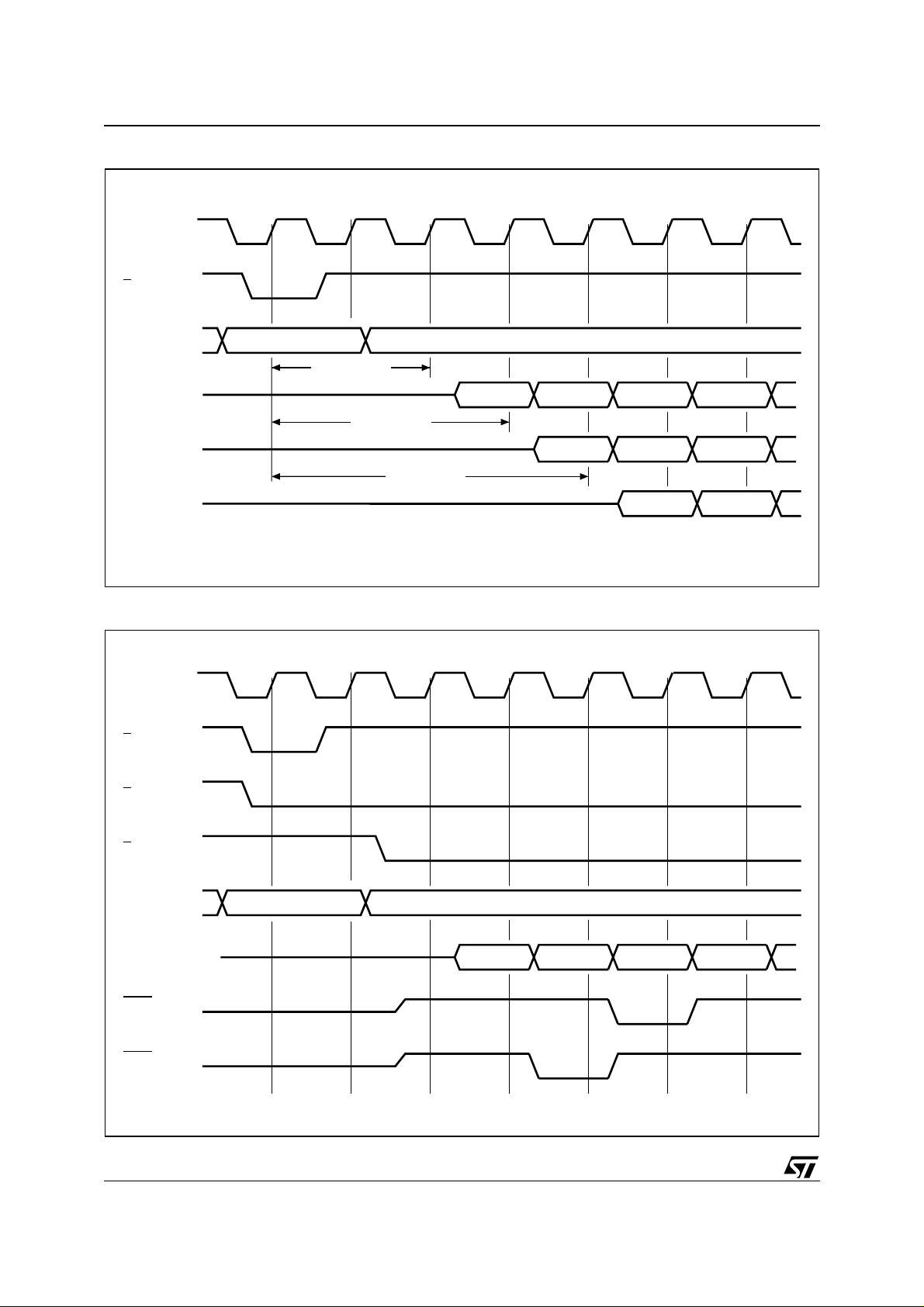
Figure 7. X-L at ency Configu ra tion Sequence
K
L
A20-A0
DQ15-DQ0
DQ15-DQ0
DQ15-DQ0
VALID ADDRESS
X latency = 2
X latency = 3
Figure 8. Wai t Co nf i gu ra tio n Sequence
K
L
X latency = 4
VALID DATA VALID DATA
VALID DATA
VALID DATA
VALID DATA
VALID DATA
VALID DATA
VALID DATA
VALID DATA
AI90105
E
G
A20-A0
DQ15-DQ0
WAIT
M8 = '0'
WAIT
M8 = '1'
18/63
VALID ADDRESS
VALID DATA
VALID DATA NOT VALID VALID DATA
AI90106

COMMAND INTERFACE
All Bus Write operations t o the me mory are in terpreted by the Command Interface. Commands
consist of one or more sequential Bus Write operations. An internal Program/Erase Controller handles all timings and verifies the correct execution
of the Program and Erase commands. The Program/Erase Controller provides a S tatus Register
whose output may be read at any time during, to
monitor the progress of the operation, or the P rogram/Erase states. See Appendix C, Tables 36
and 37, Command Interface States - Lock and
Modify Tables, for a summary of the Command Interface.
The Command Interface is reset to Read mode
when power is first applied, when exiting from Reset or whenever V
is lower than V
DD
LKO
. Command sequences must be followed exactly. Any
invalid combination of commands will reset the device to Read mode. Refer to Table 6, Commands,
in conjunction with the text descriptions below.
Read Command.
The Read command returns the addressed bank
to Read mode. One Bus Write cycle is required to
issue the Read command and return the addressed Bank to Read mode. Subsequent read
operations will read the addressed location and
output the data. A Read com mand can be issued
in one bank while programming or era sing in the
other bank. However if a Read command is issued
to a bank currently executing a program or erase
operation the command will be ignored.
When a device Reset occurs, the memory defaults
to Read mode.
Read Status Register Command
A bank’s Status Register indicates when a program or erase operation is complete and the success or failure of operation itself. Issue a Read
Status Register command to read the Status Register content of the addressed bank. The status of
the other bank is not affected by the command.
The Read Status Register command can be issued at any time, eve n during program or erase
operations.
The following Read operations output the content
of the Status Register of the addressed bank. The
Status Register is latched on the falling edge of E
or G signals, and can be read until E or G returns
to V
. Either E or G must be toggled to update the
IH
latched data. See Table 1 5 for the description of
the Status Register Bits. This mode supports
asynchronous or single synchronous reads only.
Read Electronic Signature Command
The Read Electronic Signature command reads
the Manufacturer and Device Codes and the Block
Locking Status, or the Protection Register.
M58CR032C, M58CR032D
The Read Electronic Signature command consists
of one write cycle to an address within the bot tom
bank. A subsequent read operation in the address
of the bottom bank will output the Manufacturer
Code, the Device Code, the protection Status of
Blocks of the bottom bank, the Die Revision Code,
the Protection Register, or the Read Configuration
Register (see Table 11).
If the first write cycle of Read Electronic Signature
command is issued t o an address within the top
bank, a subsequent read operat ion in an address
of the top bank will output the protection Statu s of
blocks of the top bank. The status of the other
bank is not affected by the command (see Ta ble
7). This mode supports asynchronous or single
synchronous reads only.
See Tables 8, 9, 10 and 11 for the valid addresses.
Read CFI Query Command
The Read CFI Query Command is used to read
data from the Common Flash Interface (CFI)
Memory Area, located in the bottom bank. One
Bus Write cycle, addressed to the bottom bank, is
required to issue the Read Query Command.
Once the command is issued subsequent Bus
Read operations in the bottom bank read from the
Common Flash Interface Mem ory Area. The status of the top bank is not affected by the command
(see Table 7). After issuing a Read CFI Query
command, a Read com mand should be issued to
return the bank to read mode.
See Appendix B, Common Flash Interface, Tables
29, 30, 31, 32, 33, 34 and 35 for detail s on the information contained in the Commo n Flash Interface memory area.
Clear Status Register Command
The Clear Status Register comm and c an b e us ed
to reset (set to ‘0’) bits 1, 3, 4 and 5 in the Status
Register of the addressed bank’. One bus write cycle is required to issue the Clear S tatus Register
command. After the Clear Status Register command the bank returns to read mode.
The bits in the Status Register do not automatically return to ‘0’ when a new Program or Erase command is issued. The error bits in the Status
Register should be cleared before attempting a
new Program or Erase command.
Block Erase Command
The Block Erase com mand can be used to erase
a block. It sets all the bits within the selected block
to ’1’. All previous d ata in th e block is lost. If th e
block is protected then the Erase operation will
abort, the data in the block will not be changed and
the Status Register will output the error. It is not
necessary to pre-program the block as the Pro-
19/63
 Loading...