

SGS Thomson Microelectronics M58BW016DT, M58BW016DB, M58BW016BT, M58BW016BB, M58BW016 Datasheet
1/63May 2003
M58BW016BT, M58BW016BB
M58BW016DT, M58BW016DB
16 Mb i t ( 512Kb x32, B oot Bl oc k, Bur st)
3V Supply Flash Memories
PE4FEATU R ES SUMMA R Y
■ SUPPLY VOLTAGE
–V
DD
= 2.7V to 3. 6V for Program, Erase and
Read
–V
DDQ
= V
DDQIN
= 2.4V to 3.6V for I/O Buffers
–V
PP
= 12V for fast Program (optional)
■ HIGH PERFORMANCE
– Access Time: 80, 90 and 100ns
– 56MHz Effective Zero Wait-State Burst Read
– Synchronous B urst Reads
– Asynchronous Pa ge Reads
■ HARDWARE BLOCK PROTECT ION
–W
P pin Lock Program and Erase
■ SOFTWARE BLOCK PROTECTION
– Tuning Protection to Lock Program and
Erase with 64 b it User Programmable Password (M58BW016B version only)
■ OPTIMIZED for FDI DRIVERS
– Fast Program / Erase susp end latency
time < 6µs
– Comm on Fla sh Interface
■ MEMORY BLOCKS
– 8 Parameters Blocks (Top or Bottom)
– 31 Main Blocks
■ LOW POWER CONSUMPTION
– 5µA Typical Deep Power Down
– 60µA Typic al Standby
– Automatic Standby after Asynchronous Read
■ ELECTRONIC SIGNATURE
– Manufacturer Code: 20h
– Top Device Code M58BW 016xT: 8836h
– Bottom Device Code M58BW 016x B: 8835 h
Figure 1. Packages
BGA
LBGA80 (ZA)
10 x 8 ball array
PQFP80 (T)

M58BW016BT, M58BW016BB, M58BW016D T, M58BW016DB
2/63
TABLE OF CONTENTS
SUMMARY DESCRIPTION. . . . . . . . . . . . . . . . . . . . . . . . . . . . . . . . . . . . . . . . . . . . . . . . . . . . . . . . . . . 6
Figure 2. Logic Diagram . . . . . . . . . . . . . . . . . . . . . . . . . . . . . . . . . . . . . . . . . . . . . . . . . . . . . . . . . 7
Table 1. Signal Names . . . . . . . . . . . . . . . . . . . . . . . . . . . . . . . . . . . . . . . . . . . . . . . . . . . . . . . . . . 7
Figure 3. LBGA Connections (Top view through package) . . . . . . . . . . . . . . . . . . . . . . . . . . . . . . . 8
Figure 4. PQFP Connections (Top view through package). . . . . . . . . . . . . . . . . . . . . . . . . . . . . . . 9
Block Protection . . . . . . . . . . . . . . . . . . . . . . . . . . . . . . . . . . . . . . . . . . . . . . . . . . . . . . . . . . . . . . 10
Tuning Block Protection. . . . . . . . . . . . . . . . . . . . . . . . . . . . . . . . . . . . . . . . . . . . . . . . . . . . . . . . . . 10
Table 2. Top Boot Block Addresses, M58BW016B T, M58BW016DT . . . . . . . . . . . . . . . . . . . . . . 11
Table 3. Bottom Boot Block Addresses, M58BW016B B , M58BW016DB . . . . . . . . . . . . . . . . . . . 12
SIGNAL DESCRIPTIONS . . . . . . . . . . . . . . . . . . . . . . . . . . . . . . . . . . . . . . . . . . . . . . . . . . . . . . . . . . . 13
Address Inputs (A0-A18). . . . . . . . . . . . . . . . . . . . . . . . . . . . . . . . . . . . . . . . . . . . . . . . . . . . . . . . . 13
Data Inputs/Outputs (DQ0-DQ31 ). . . . . . . . . . . . . . . . . . . . . . . . . . . . . . . . . . . . . . . . . . . . . . . . . .13
Chip Enable (E). . . . . . . . . . . . . . . . . . . . . . . . . . . . . . . . . . . . . . . . . . . . . . . . . . . . . . . . . . . . . . . . 13
Output Enable (G). . . . . . . . . . . . . . . . . . . . . . . . . . . . . . . . . . . . . . . . . . . . . . . . . . . . . . . . . . . . . . 13
Output Disable (GD).. . . . . . . . . . . . . . . . . . . . . . . . . . . . . . . . . . . . . . . . . . . . . . . . . . . . . . . . . . . . 13
Write Enable (W). . . . . . . . . . . . . . . . . . . . . . . . . . . . . . . . . . . . . . . . . . . . . . . . . . . . . . . . . . . . . . . 13
Reset/Power-Down (RP). . . . . . . . . . . . . . . . . . . . . . . . . . . . . . . . . . . . . . . . . . . . . . . . . . . . . . . . . 13
Latch Enable (L).. . . . . . . . . . . . . . . . . . . . . . . . . . . . . . . . . . . . . . . . . . . . . . . . . . . . . . . . . . . . . . . 13
Burst Clock (K).. . . . . . . . . . . . . . . . . . . . . . . . . . . . . . . . . . . . . . . . . . . . . . . . . . . . . . . . . . . . . . . . 14
Burst Address Advance (B). . . . . . . . . . . . . . . . . . . . . . . . . . . . . . . . . . . . . . . . . . . . . . . . . . . . . . . 14
Valid Data Ready (R). . . . . . . . . . . . . . . . . . . . . . . . . . . . . . . . . . . . . . . . . . . . . . . . . . . . . . . . . . . . 14
Write Protect (WP). . . . . . . . . . . . . . . . . . . . . . . . . . . . . . . . . . . . . . . . . . . . . . . . . . . . . . . . . . . . . . 14
Supply Volt a g e (V
DD)
. . . . . . . . . . . . . . . . . . . . . . . . . . . . . . . . . . . . . . . . . . . . . . . . . . . . . . . . . . . . 14
Output Supply Voltage (V
DDQ
). . . . . . . . . . . . . . . . . . . . . . . . . . . . . . . . . . . . . . . . . . . . . . . . . . . . . 14
Input Supply Voltage (V
DDQIN
) . . . . . . . . . . . . . . . . . . . . . . . . . . . . . . . . . . . . . . . . . . . . . . . . . . . .14
Program/Erase Supply Voltage (V
PP
).. . . . . . . . . . . . . . . . . . . . . . . . . . . . . . . . . . . . . . . . . . . . . . . 14
Ground (V
SS
and V
SSQ
). . . . . . . . . . . . . . . . . . . . . . . . . . . . . . . . . . . . . . . . . . . . . . . . . . . . . . . . . . 14
BUS OPERATIONS. . . . . . . . . . . . . . . . . . . . . . . . . . . . . . . . . . . . . . . . . . . . . . . . . . . . . . . . . . . . . . . . 15
Asynchronous Bus Operations . . . . . . . . . . . . . . . . . . . . . . . . . . . . . . . . . . . . . . . . . . . . . . . . . . 15
Asynchronous Bus Read. . . . . . . . . . . . . . . . . . . . . . . . . . . . . . . . . . . . . . . . . . . . . . . . . . . . . . . . . 1 5
Asynchronous Latch Controlled Bus Read . . . . . . . . . . . . . . . . . . . . . . . . . . . . . . . . . . . . . . . . . . . 15
Asynchronous Page Read. . . . . . . . . . . . . . . . . . . . . . . . . . . . . . . . . . . . . . . . . . . . . . . . . . . . . . . . 15
Asynchronous Bus Write . . . . . . . . . . . . . . . . . . . . . . . . . . . . . . . . . . . . . . . . . . . . . . . . . . . . . . . . . 15
Asynchronous Latch Controlled Bus Write . . . . . . . . . . . . . . . . . . . . . . . . . . . . . . . . . . . . . . . . . . . 15
Output Disable. . . . . . . . . . . . . . . . . . . . . . . . . . . . . . . . . . . . . . . . . . . . . . . . . . . . . . . . . . . . . . . . . 16
Standby . . . . . . . . . . . . . . . . . . . . . . . . . . . . . . . . . . . . . . . . . . . . . . . . . . . . . . . . . . . . . . . . . . . . . . 16
Automatic Low Power.. . . . . . . . . . . . . . . . . . . . . . . . . . . . . . . . . . . . . . . . . . . . . . . . . . . . . . . . . . . 16
Power-Down.. . . . . . . . . . . . . . . . . . . . . . . . . . . . . . . . . . . . . . . . . . . . . . . . . . . . . . . . . . . . . . . . . . 1 6
Electronic Signature. . . . . . . . . . . . . . . . . . . . . . . . . . . . . . . . . . . . . . . . . . . . . . . . . . . . . . . . . . . . . 16
Table 4. Asynchronous Bus Operations . . . . . . . . . . . . . . . . . . . . . . . . . . . . . . . . . . . . . . . . . . . . 16
Table 5. Asynchronous Read Electronic Signature Operation . . . . . . . . . . . . . . . . . . . . . . . . . . . 17

3/63
M58BW016BT, M58BW016BB, M58BW016DT, M58BW016DB
Synchronous Bus Operations . . . . . . . . . . . . . . . . . . . . . . . . . . . . . . . . . . . . . . . . . . . . . . . . . . .17
Synchronous Burst Read. . . . . . . . . . . . . . . . . . . . . . . . . . . . . . . . . . . . . . . . . . . . . . . . . . . . . . . . . 17
Synchronous Burst Read Suspend . . . . . . . . . . . . . . . . . . . . . . . . . . . . . . . . . . . . . . . . . . . . . . . . . 17
Table 6. Synchronous Burst Read Bus Operations. . . . . . . . . . . . . . . . . . . . . . . . . . . . . . . . . . . . 18
Burst Configuration Register. . . . . . . . . . . . . . . . . . . . . . . . . . . . . . . . . . . . . . . . . . . . . . . . . . . . 19
Read Select Bit (M15) . . . . . . . . . . . . . . . . . . . . . . . . . . . . . . . . . . . . . . . . . . . . . . . . . . . . . . . . . . . 19
X-Latency Bits (M14-M11). . . . . . . . . . . . . . . . . . . . . . . . . . . . . . . . . . . . . . . . . . . . . . . . . . . . . . . . 19
Y-Latency Bit (M9). . . . . . . . . . . . . . . . . . . . . . . . . . . . . . . . . . . . . . . . . . . . . . . . . . . . . . . . . . . . . . 19
Valid Data Ready Bit (M8). . . . . . . . . . . . . . . . . . . . . . . . . . . . . . . . . . . . . . . . . . . . . . . . . . . . . . . . 19
Burst Type Bit (M7).. . . . . . . . . . . . . . . . . . . . . . . . . . . . . . . . . . . . . . . . . . . . . . . . . . . . . . . . . . . . . 19
Valid Clock Edge Bit (M6).. . . . . . . . . . . . . . . . . . . . . . . . . . . . . . . . . . . . . . . . . . . . . . . . . . . . . . . . 19
Wrap Burst Bit (M3). . . . . . . . . . . . . . . . . . . . . . . . . . . . . . . . . . . . . . . . . . . . . . . . . . . . . . . . . . . . . 19
Burst Length Bit (M2-M0).. . . . . . . . . . . . . . . . . . . . . . . . . . . . . . . . . . . . . . . . . . . . . . . . . . . . . . . . 19
Table 7. Burst Configuration Register . . . . . . . . . . . . . . . . . . . . . . . . . . . . . . . . . . . . . . . . . . . . . . 20
Table 8. Burst Type Definition. . . . . . . . . . . . . . . . . . . . . . . . . . . . . . . . . . . . . . . . . . . . . . . . . . . . 21
COMMAND INTERFACE. . . . . . . . . . . . . . . . . . . . . . . . . . . . . . . . . . . . . . . . . . . . . . . . . . . . . . . . . . 23
Read Memory Array Command. . . . . . . . . . . . . . . . . . . . . . . . . . . . . . . . . . . . . . . . . . . . . . . . . . . .23
Read Electronic Signature Comma nd . . . . . . . . . . . . . . . . . . . . . . . . . . . . . . . . . . . . . . . . . . . . . . . 23
Read Query Command . . . . . . . . . . . . . . . . . . . . . . . . . . . . . . . . . . . . . . . . . . . . . . . . . . . . . . . . . . . 23
Read Status Register Command. . . . . . . . . . . . . . . . . . . . . . . . . . . . . . . . . . . . . . . . . . . . . . . . . . .23
Clear Status Register Command. . . . . . . . . . . . . . . . . . . . . . . . . . . . . . . . . . . . . . . . . . . . . . . . . . . 23
Block Erase Command . . . . . . . . . . . . . . . . . . . . . . . . . . . . . . . . . . . . . . . . . . . . . . . . . . . . . . . . . . 23
Program Command. . . . . . . . . . . . . . . . . . . . . . . . . . . . . . . . . . . . . . . . . . . . . . . . . . . . . . . . . . . . . 24
Program/Erase Suspend Comm and . . . . . . . . . . . . . . . . . . . . . . . . . . . . . . . . . . . . . . . . . . . . . . . . 24
Program/Erase Resume Command . . . . . . . . . . . . . . . . . . . . . . . . . . . . . . . . . . . . . . . . . . . . . . . . 24
Set Burst Configuration Register Command. . . . . . . . . . . . . . . . . . . . . . . . . . . . . . . . . . . . . . . . . . 24
Tuning Protection Unlock Command. . . . . . . . . . . . . . . . . . . . . . . . . . . . . . . . . . . . . . . . . . . . . . . .25
Tuning Protection Program Command.. . . . . . . . . . . . . . . . . . . . . . . . . . . . . . . . . . . . . . . . . . . . . . 25
Table 9. Commands . . . . . . . . . . . . . . . . . . . . . . . . . . . . . . . . . . . . . . . . . . . . . . . . . . . . . . . . . . . 26
Table 10. Program, Erase Times and Program Erase Endurance Cycles . . . . . . . . . . . . . . . . . . 27
STATUS REGISTER. . . . . . . . . . . . . . . . . . . . . . . . . . . . . . . . . . . . . . . . . . . . . . . . . . . . . . . . . . . . . . . 28
Program/Erase Controller Status (Bit 7) . . . . . . . . . . . . . . . . . . . . . . . . . . . . . . . . . . . . . . . . . . . . .28
Erase Suspend Status (Bit 6) . . . . . . . . . . . . . . . . . . . . . . . . . . . . . . . . . . . . . . . . . . . . . . . . . . . . . 28
Erase Status (Bit 5) . . . . . . . . . . . . . . . . . . . . . . . . . . . . . . . . . . . . . . . . . . . . . . . . . . . . . . . . . . . . . 28
Program Status, Tuning Protection Unlock Status (Bit 4) . . . . . . . . . . . . . . . . . . . . . . . . . . . . . . . . 28
V
PP
Status (Bit 3). . . . . . . . . . . . . . . . . . . . . . . . . . . . . . . . . . . . . . . . . . . . . . . . . . . . . . . . . . . . . . . 28
Program Suspend Status (Bit 2) . . . . . . . . . . . . . . . . . . . . . . . . . . . . . . . . . . . . . . . . . . . . . . . . . . . 29
Block Protection Status (Bit 1). . . . . . . . . . . . . . . . . . . . . . . . . . . . . . . . . . . . . . . . . . . . . . . . . . . . . 29
Tuning Protection Status (Bit 0). . . . . . . . . . . . . . . . . . . . . . . . . . . . . . . . . . . . . . . . . . . . . . . . . . . . 29
Table 11. Status Register Bits. . . . . . . . . . . . . . . . . . . . . . . . . . . . . . . . . . . . . . . . . . . . . . . . . . . . 29
MAXIMUM RATING. . . . . . . . . . . . . . . . . . . . . . . . . . . . . . . . . . . . . . . . . . . . . . . . . . . . . . . . . . . . . . . . 30
Table 12. Absolute Maximum Ratings. . . . . . . . . . . . . . . . . . . . . . . . . . . . . . . . . . . . . . . . . . . . . . 30

M58BW016BT, M58BW016BB, M58BW016D T, M58BW016DB
4/63
DC and AC PARAMETERS . . . . . . . . . . . . . . . . . . . . . . . . . . . . . . . . . . . . . . . . . . . . . . . . . . . . . . . . . 31
Table 13. Operating and AC Measurement Conditions. . . . . . . . . . . . . . . . . . . . . . . . . . . . . . . . . 31
Figure 7. AC Measurement Input Output Waveform . . . . . . . . . . . . . . . . . . . . . . . . . . . . . . . . . . . 31
Figure 8. AC Measurement Load Circuit . . . . . . . . . . . . . . . . . . . . . . . . . . . . . . . . . . . . . . . . . . . . 31
Table 14. Device Capacitance. . . . . . . . . . . . . . . . . . . . . . . . . . . . . . . . . . . . . . . . . . . . . . . . . . . . 31
Table 15. DC Characteristics. . . . . . . . . . . . . . . . . . . . . . . . . . . . . . . . . . . . . . . . . . . . . . . . . . . . . 32
Figure 9. Asynchronous Bus Read AC Waveforms. . . . . . . . . . . . . . . . . . . . . . . . . . . . . . . . . . . . 33
Table 16. Asynchronous Bus Read AC Characteristics. . . . . . . . . . . . . . . . . . . . . . . . . . . . . . . . . 33
Figure 10. Asynchronous Latch Controlled Bus Read AC Waveforms . . . . . . . . . . . . . . . . . . . . . 34
Table 17. Asynchronous Latch Controlled Bus Read AC Characteristics. . . . . . . . . . . . . . . . . . . 34
Figure 11. Asynchronous Page Read AC Waveforms . . . . . . . . . . . . . . . . . . . . . . . . . . . . . . . . . 35
Table 18. Asynchronous Page Read AC Characteristics . . . . . . . . . . . . . . . . . . . . . . . . . . . . . . . 35
Figure 12. Asynchronous Write AC Waveform . . . . . . . . . . . . . . . . . . . . . . . . . . . . . . . . . . . . . . . 36
Figure 13. Asynchronous Latch Controlled Write AC Waveform . . . . . . . . . . . . . . . . . . . . . . . . . . 37
Table 19. Asynchronous Write and Latch Controlled Write AC Characteristics . . . . . . . . . . . . . . 38
Figure 14. Synchronous Burst Read (Data Valid from ’n’ Clock Rising Edge) . . . . . . . . . . . . . . . 39
Table 20. Synchronous Burst Read AC Characteristics . . . . . . . . . . . . . . . . . . . . . . . . . . . . . . . . 40
Figure 15. Synchronous Burst Read (Data Valid from ’n’ Clock Rising Edge) . . . . . . . . . . . . . . . 40
Figure 16. Synchronous Burst Read - Continuous - Valid Data Ready Output. . . . . . . . . . . . . . . 41
Figure 17. Synchronous Burst Read - Burst Address Advance. . . . . . . . . . . . . . . . . . . . . . . . . . . 41
Figure 18. Reset, Power-Down and Power-up AC Waveform. . . . . . . . . . . . . . . . . . . . . . . . . . . . 42
Table 21. Reset, Power-Down and Power-up AC Characteristics . . . . . . . . . . . . . . . . . . . . . . . . 42
PACKAGE MECHANICAL . . . . . . . . . . . . . . . . . . . . . . . . . . . . . . . . . . . . . . . . . . . . . . . . . . . . . . . . . . 4 3
Figure 19. LBGA80 10x12mm - 8x10 ball array, 1mm pitch, Bottom View Package Outlin e . . . . 43
Table 22. LBGA80 10x12mm - 8x10 ball array, 1mm pitch, Package Mecha nical Data . . . . . . . . 43
Figure 20. PQFP80 - 80 lead Plastic Quad Flat Pack, Package Outline. . . . . . . . . . . . . . . . . . . . 44
Table 23. PQFP80 - 80 lead Plastic Quad Flat Pack, Package Mechanical Data. . . . . . . . . . . . . 44
PART NUMBERING . . . . . . . . . . . . . . . . . . . . . . . . . . . . . . . . . . . . . . . . . . . . . . . . . . . . . . . . . . . . . . . 45
Table 24. Ordering Information Scheme . . . . . . . . . . . . . . . . . . . . . . . . . . . . . . . . . . . . . . . . . . . . 45
APPENDIX A. COMMON FLASH INTERFACE - CFI. . . . . . . . . . . . . . . . . . . . . . . . . . . . . . . . . . . . . 46
Table 25. Query Structure Overview. . . . . . . . . . . . . . . . . . . . . . . . . . . . . . . . . . . . . . . . . . . . . . . 46
Table 26. CFI - Query Address and Data Output . . . . . . . . . . . . . . . . . . . . . . . . . . . . . . . . . . . . . 46
Table 27. CFI - Device Voltage and Timing Specification. . . . . . . . . . . . . . . . . . . . . . . . . . . . . . . 47
Table 28. Device Geometry Definition. . . . . . . . . . . . . . . . . . . . . . . . . . . . . . . . . . . . . . . . . . . . . . 47
Table 29. Extended Query information . . . . . . . . . . . . . . . . . . . . . . . . . . . . . . . . . . . . . . . . . . . . . 48
APPENDIX B. FLOW CHARTS . . . . . . . . . . . . . . . . . . . . . . . . . . . . . . . . . . . . . . . . . . . . . . . . . . . . . 49
Figure 21. Program Flowchart and Pseudo Code . . . . . . . . . . . . . . . . . . . . . . . . . . . . . . . . . . . . . 49
Figure 22. Program Suspend & Resume Flowchart and Pseudo Code . . . . . . . . . . . . . . . . . . . . 50
Figure 23. Block Erase Flowchart and Pseudo Code . . . . . . . . . . . . . . . . . . . . . . . . . . . . . . . . . . 51
Figure 24. Erase Suspend & Resume Flowchart and Pseudo Code. . . . . . . . . . . . . . . . . . . . . . . 52
Figure 25. Unlock Device and Change Tuning Protection Code Flowchart . . . . . . . . . . . . . . . . . 53

5/63
M58BW016BT, M58BW016BB, M58BW016DT, M58BW016DB
Figure 26. Unlock Device and Program a Tuning Protected Block Flowchart. . . . . . . . . . . . . . . . 54
Figure 27. Unlock Device and Erase a Tuning Protected Block Flowchart. . . . . . . . . . . . . . . . . . 55
Figure 28. Power-up Sequence to Burst the Flash . . . . . . . . . . . . . . . . . . . . . . . . . . . . . . . . . . . . 56
Figure 29. Command Interface and Program Erase Controller Flowchart (a). . . . . . . . . . . . . . . . 57
Figure 30. Command Interface and Program Erase Controller Flowchart (b). . . . . . . . . . . . . . . . 58
Figure 31. Command Interface and Program Erase Controller Flowchart (c) . . . . . . . . . . . . . . . . 59
Figure 32. Command Interface and Program Erase Controller Flowchart (d). . . . . . . . . . . . . . . . 60
Figure 33. Command Interface and Program Erase Controller Flowchart (e). . . . . . . . . . . . . . . . 61
REVISION HISTORY . . . . . . . . . . . . . . . . . . . . . . . . . . . . . . . . . . . . . . . . . . . . . . . . . . . . . . . . . . . . . . . 62
Table 30. Document Revision History. . . . . . . . . . . . . . . . . . . . . . . . . . . . . . . . . . . . . . . . . . . . . . 62

M58BW016BT, M58BW016BB, M58BW016D T, M58BW016DB
6/63
SUMMARY DESCRIPTION
The M58BW016B/D is a 16Mbit non-volatile Flash
memory that can be erased electrically at the block
level and programmed in-system on a DoubleWord basis using a 2.7V to 3.6V V
DD
supply for the
circuit and a V
DDQ
supply down to 2.4V for the In-
put and Output buffers. Optionally a 12V V
PP
supply can be used to provide fast program and erase
for a limited time and number of program/erase cycles.
The devices support Asynchronous (Latch Controlled and Page Read) and Synchronous Bus operations. The Synchronous B urst Read Interface
allows a high data tra nsfer rate controlled by the
Burst Clock, K, signal. It is capable of bursting
fixed or unlimited lengths of data. The burst type,
latency and length are configurable and can be
easily adapted to a large variety of system clock
frequencies and microprocessors. All Writes are
Asynchronous. On power-up the memory defaults
to Read mode with an Asynchronous Bus.
The device has a boot block architecture with an
array of 8 parameter bl ock of 64Kb each and 31
main blocks of 512Kb each. The parameter blocks
can be located at the top of the address space,
M58BW016BT, M58BW016DT or at the bottom,
M58BW016BB, M58B W016DB.
Program and Erase c ommands are written to the
Command Interface of the memory. An on-chip
Program/Erase Controller simplifies the process of
programming or erasing the memory by taking
care of all of the special operations that are required to update the memory contents. The end of
a Program or Erase operation can be detected and
any error conditions identified in the Status Regis-
ter. The command set required to control the
memory is consistent with JEDEC standards.
Erase can be suspended in order to perform either
Read or Program in any other block and t hen resumed. Program can be suspended t o Read dat a
in any other block and t hen resumed. E ach block
can be programmed and erased over 100,000 cycles.
All blocks are protected during power-up. The
M58BW016B features four different levels of block
protection to avoid unwanted program/erase operations. The WP
pin offers an hardware protect ion
on two of the parameter blocks and all of the main
blocks. The Program and Erase commands can
be password protected by the Tuning Protection
command. All Program or Erase operations are
blocked when Reset, RP,
is held low. The
M58BW016D offers the same protection features
with the exception of the Tuning Block Protection
which is disabled in the factory.
A Reset/Power-down mode is entered w hen the
RP
input is Low. In this mode the power consumption is lower than in the normal standby mode, the
device is write protect ed and bo th the S tatus and
the Burst Configuration Registers are cleared. A
recovery time is required when th e RP
input goes
High.
The memory is offered in PQFP80 (14 x 20mm)
and LBGA80 (1.0mm pitch) packages and it is
supplied with all the bits erased (set to ’1’).
7/63
M58BW016BT, M58BW016BB, M58BW016DT, M58BW016DB
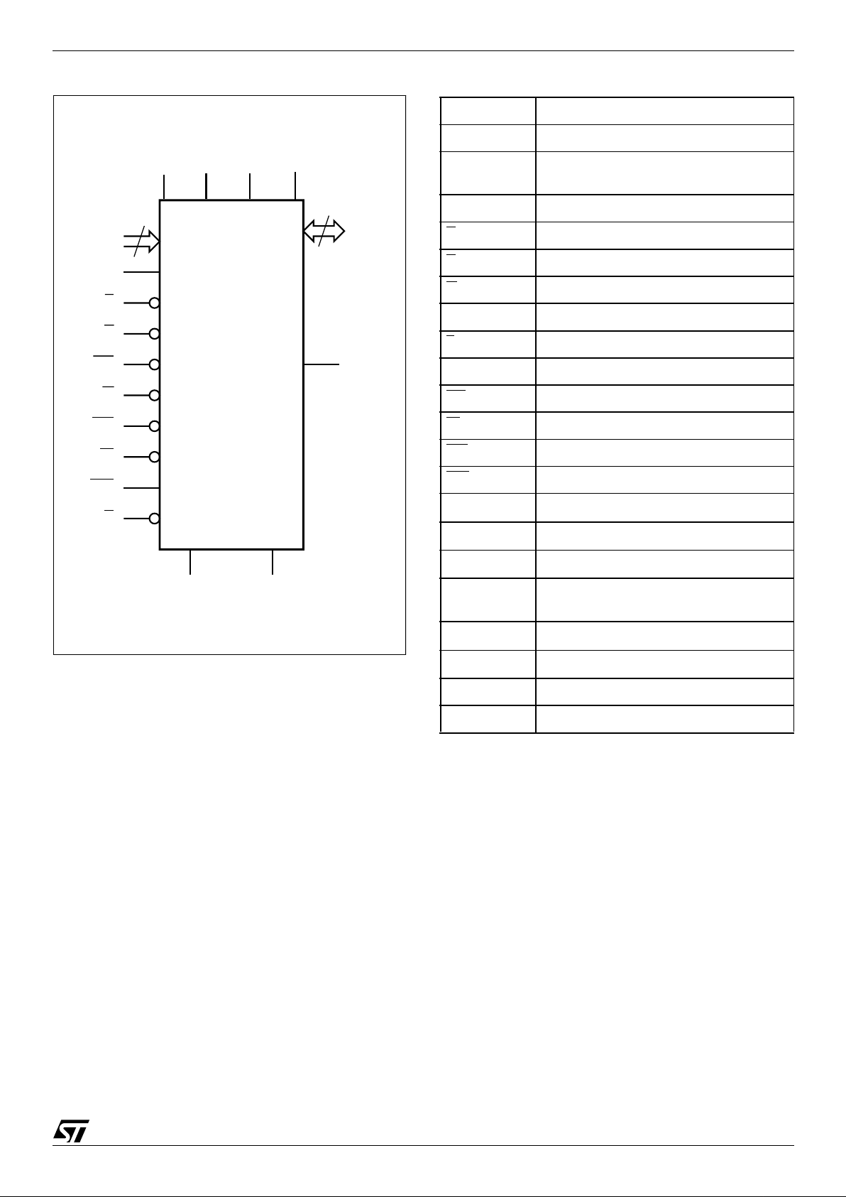
Figure 2. Logic Diagram Table 1. Signal Names
AI04155
A0-A18
L
DQ0-DQ31
V
DD
M58BW016DT
M58BW016DB
E
V
SS
RP
G
GD
V
DDQ
W
WP
R
K
V
PP
B
V
SSQ
V
DDQIN
M58BW016BT
M58BW016BB
A0-A18 Address inputs
DQ0-DQ7 Data Input/Output, Command Input
DQ8-DQ15
Data Input/Output, Burst Configuration
Register
DQ16-DQ31 Data Input/Output
B
Burst Address Advance
E
Chip Enable
G
Output Enable
K Burst Clock
L
Latch Enable
R Valid Data Ready (open drain output)
RP
Reset/Power-down
W
Write Enable
GD
Output Disable
WP
Write Protect
V
DD
Supply Voltage
V
DDQ
Power Supply for Output Buffers
V
DDQIN
Power Supply for Input Buffers only
V
PP
Optional Supply Voltage for Fast
Program and Fast Erase Operations
V
SS
Ground
V
SSQ
Input/Output Ground
NC Not Connected Internally
DU Don’t Use as Internally Connected
M58BW016BT, M58BW016BB, M58BW016D T, M58BW016DB
8/63
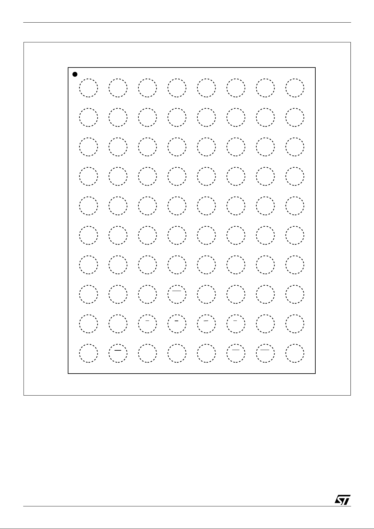
Figure 3. LBGA Conn ec ti ons (Top view through package)
AI04151b
B
DQ24DQ7V
SSQ
F
V
DDQ
DQ26DQ4V
DDQ
E
DQ29
V
SS
DQ0DQ3D
A0
DUA7A11A18A17C
A1
A4A5A8
RP
E
A13A16B
A2
A3A6
V
DD
V
PP
V
DD
A14A
87654321
DQ20DQ18DQ19DQ17DQ11DQ12DQ13
V
DDQ
DQ23DQ8V
DDQ
H
G
DU
GDW
V
DDQIN
DQ16RGLDQ14DQ15
K
J
A15 V
SS
A12 A9
A10 NC
DU DU DQ31 DQ30
DQ2 DQ28
DQ6 DQ25 V
SSQ
DQ10 DQ9 DQ21
WP
K
DU
DQ1 DQ27
DQ5 NC
DQ22
9/63
M58BW016BT, M58BW016BB, M58BW016DT, M58BW016DB
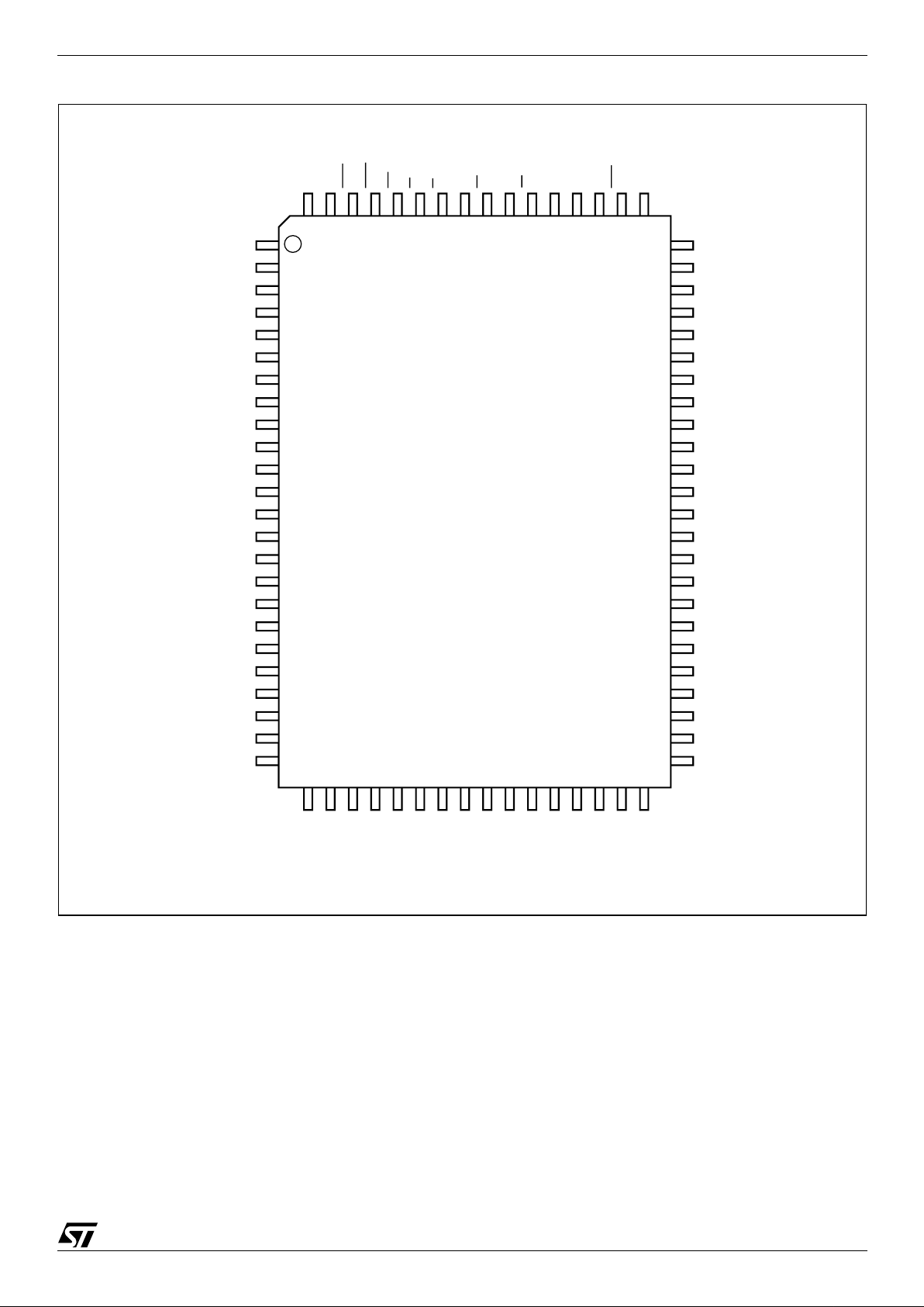
Figure 4. PQFP Connections (Top view through package)
AI04152b
12
1
73
M58BW016BT
M58BW016BB
53
V
DDQ
DQ24
DQ25
DQ18
DQ17
DQ16
DQ19
DQ20
DQ21
DQ22
DQ23
V
DDQ
DQ29
DQ26
DQ30
DU
DQ31
DQ28
DQ27
A2
A5
A3
A4
A0
A1
A11
V
SS
A12
A13
A14
A10
GDWPWDUG
V
SS
E
K
L
NC
B
RP
V
DDQ
DQ7
DQ6
DQ13
DQ14
DQ15
DQ12
DQ11
DQ10
DQ9
V
SSQ
DQ8
DQ2
DQ5
DQ0
NC
A18
A16
A17
DQ3
DQ4
V
SSQ
V
SSQ
A8
A6
A7
V
PP
V
DD
A9
A15
DQ1
V
DDQ
V
SSQ
R
V
DD
NC
V
DDQIN
24
25
32
40
41
64
65
80
M58BW016DT
M58BW016DB

M58BW016BT, M58BW016BB, M58BW016D T, M58BW016DB
10/63
Block Protection
The M58BW016B fe atures four different levels of
block protection. The M58BW016D h as the same
block protection with the exception of the Tuning
Block Protection, which is disabled in the factory.
■ Write Protect Pin, WP, - When WP is low, V
IL,
all the lockable parameter blocks (two upper
(Top ) or lower (B ottom)) and all the main blocks
are protected. When WP
is high (VIH) all the
lockable paramete r blocks a nd all the main
blocks are unprotected.
■ Reset/Power-Down Pin, RP, - If the device is
held in reset mode (RP
at VIL), no program or
erase operations can be performed on any
block.
■ Tuning Block Protection: M58BW016B
features a 64 bit password protection for
program and erase operations for a fixed
number of blocks After power-up or reset the
device is tuning protected. An Unlock command
is provided to allow program or erase operations
in all the blocks.
Aft er a de v i ce r es et t h e f i r st t w o k i nds of bl ock p r otection (W
P, RP) c an be c om bin ed t o give a flexible block protection. They do not affect the Tuning
Block Protection. When the two protections are
disabled, W
P and RP at VIH, the blocks locked by
the Tuning Block Protection cannot be modified.
All blocks are protected during power-up.
Tuning Bl ock P rot ection. The Tuning Block
Protection is a software f eature to protect certain
blocks from program or erase operat ions. It allo ws
the user to lock program and erase operations with
a user definable 64 bit code. It is only available on
the M58BW016B version.
The code is written once i n the Tuning Protection
Register and cannot be erased. When shipped the
flash memory will have the Tuning Protection
Code bits set to ‘1'. The user can program a ‘0’ in
any of the 64 positions. Once programmed it is not
possible to reset a bit t o ‘ 1’ a s the cells cannot be
erased. The Tuning Protection Register can be
programmed at any moment (after providing the
correct code), however once all bits are set to ‘0’
the Tuning Protection Code can no longer be altered .
The Tuning Protection Code locks the program
and erase operations of 2 parameter and 24 main
blocks, blocks 0, 1 and 15-38 for the bottom configuration and the blocks 0-23, 3 7 and 38 for the
top configuration.
The tuning b locks ar e "lo cked" if th e tuni ng pr otection code has not been provided, and “unlock ed"
once the correct code has been provided. The tuning blocks are locked af te r rese t o r power-u p. The
tuning protection status can be monitored in the
Status Register. Refer to the Status Register section.
Refer to the Command Interface section for the
Tuning Protection Block Un lock and Tuning Protection Program commands. See Appendix B, Figure 25, 26 and 27 for suggested flowcharts for
using the Tuning Block Protection commands. For
further information on the Tuning Block Protection
refer to Application Note, AN1361.
11/63
M58BW016BT, M58BW016BB, M58BW016DT, M58BW016DB
Table 2. Top Boot Block Addresses,
M58BW016BT, M58BW016DT
Note: 1. TP = Tuning Protected Block, only available for the
M58BW016B.
# Size (Kbit) Address Range
TP
(1)
38 64 7F800h-7FFFFh yes
37 64 7F000h-7F7FFh yes
36 64 7E800h-7EFFFh no
35 64 7E000h-7E7FFh no
34 64 7D800h-7DFFFh no
33 64 7D000h-7D7FFh no
32 64 7C800h-7CFFFh no
31 64 7C000h-7C7FFh no
30 512 78000h-7BFFFh no
29 512 74000h-77FFFh no
28 512 70000h-73FFFh no
27 512 6C000h-6FFFFh no
26 512 68000h-6BFFFh no
25 512 64000h-67FFFh no
24 512 60000h-63FFFh no
23 512 5C000h-5FFFFh yes
22 512 58000h-5BFFFh yes
21 512 54000h-57FFFh yes
20 512 50000h-53FFFh yes
19 512 4C000h-4FFFFh yes
18 512 48000h-4BFFFh yes
17 512 44000h-47FFFh yes
16 512 40000h-43FFFh yes
15 512 3C000h-3FFFFh yes
14 512 38000h-3BFFFh yes
13 512 34000h-37FFFh yes
12 512 30000h-33FFFh yes
11 512 2C000h-2FFFFh yes
10 512 28000h-2BFFFh yes
9 512 24000h-27FFFh yes
8 512 20000h-23FFFh yes
7 512 1C000h-1FFFFh yes
6 512 18000h-1BFFFh yes
5 512 14000h-17FFFh yes
4 512 10000h-13FFFh yes
3 512 0C000h-0FFFFh yes
2 512 08000h-0BFFFh yes
1 512 04000h-07FFFh yes
0 512 00000h-03FFFh yes
# Size (Kbit) Address Range
TP
(1)
M58BW016BT, M58BW016BB, M58BW016D T, M58BW016DB
12/63
Table 3. Bottom Boot Block Addresses,
M58BW016BB, M58BW016DB
Note: 1. TP = Tuning Protected Block, only available for the
M58BW016B.
# Size (Kbit) Address Range
TP
(1)
38 512 7C000h-7FFFFh yes
37 512 78000h-7BFFFh yes
36 512 74000h-77FFFh yes
35 512 70000h-73FFFh yes
34 512 6C000h-6FFFFh yes
33 512 68000h-6BFFFh yes
32 512 64000h-67FFFh yes
31 512 60000h-63FFFh yes
30 512 5C000h-5FFFFh yes
29 512 58000h-5BFFFh yes
28 512 54000h-57FFFh yes
27 512 50000h-53FFFh yes
26 512 4C000h-4FFFFh yes
25 512 48000h-4BFFFh yes
24 512 44000h-47FFFh yes
23 512 40000h-43FFFh yes
22 512 3C000h-3FFFFh yes
21 512 38000h-3BFFFh yes
20 512 34000h-37FFFh yes
19 512 30000h-33FFFh yes
18 512 2C000h-2FFFFh yes
17 512 28000h-2BFFFh yes
16 512 24000h-27FFFh yes
15 512 20000h-23FFFh yes
14 512 1C000h-1FFFFh no
13 512 18000h-1BFFFh no
12 512 14000h-17FFFh no
11 512 10000h-13FFFh no
10 512 0C000h-0FFFFh no
9 512 08000h-0BFFFh no
8 512 04000h-07FFFh no
7 64 03800h-03FFFh no
6 64 03000h-037FFh no
5 64 02800h-02FFFh no
4 64 02000h-027FFh no
3 64 01800h-01FFFh no
2 64 01000h-017FFh no
1 64 00800h-00FFFh yes
0 64 00000h-007FFh yes
# Size (Kbit) Address Range
TP
(1)

13/63
M58BW016BT, M58BW016BB, M58BW016DT, M58BW016DB
SIGNAL DESCRIPTIONS
See Figure 2, Logic Diagram and Table 1, Signal
Names, for a brief overview of the signals connected to this device.
Address Inputs (A0-A18). The Address Inputs
are used to select the cells to access in the mem ory array during Bus Read operations either to
read or to program data to. During Bus Write operations they control the commands sent to the
Command Interface of the internal state m achine.
Chip Enable must be low when selecting the addresses.
The address inputs are latched on the rising edge
of Latch Enable L
or Burst Clock K, whichever occurs first, in a read operation.The address inputs
are latched on the rising edge of Chip Enable,
Write Enable or Lat ch Enable, whichever o ccurs
first in a Write operation. The address latch is
transparent when Latch Enable is low, V
IL
. The address is internally latched in a n E rase or P rogram
operation.
Data Inputs/Outputs (DQ0-DQ31). The Data Inputs/Outputs output the data stored at the selected
address during a Bus Read operation, or are used
to input the data during a program operation. During Bus Write operations they represent the commands sent to the Command Interface of the
internal state machine. When used to input data or
Write commands they are latched on the rising
edge of Write Enable or Chip Enable, whichever
occurs first.
When Chip Enable and Output Enable are both
low, V
IL
, and Output Disable is at V
IH,
the data bus
outputs data from the memory array, the Electronic Signature, the CFI Information or the contents of
the Status Register. The data bus is high impedance when the device is deselected with Chip Enable at V
IH
, Output E na ble at VIH, Outp u t Di sa b le
at V
IL
or Reset/Power-Down at VIL. The Status
Register content is output on DQ0-DQ7 and DQ8DQ31 are at V
IL
.
Chip Enable (E
). The Chip Enable, E, input acti-
vates the memory control logic, input buffers, decoders and sense amplifiers. Chip Enable, E
, at
V
IH
deselects the memory and reduces the power
consumption to the Standby level.
Output Enable (G
). The Output Enable, G, gates
the outputs through the data output buffers during
a read operation, whe n Output Disable GD
is at
V
IH
. When Output Enable G is at VIH, the outputs
are high impedance in dependentl y of Output Disable.
Output Disable (GD
). The Output Disable, GD,
deactivates the data output buffers. W hen Output
Disable, GD
, is at VIH, the outputs are driven by
the Output Enable. When Output Disable, GD
, is at
V
IL
, the outputs are high impedance independent-
ly of Output Enable. The Output Disable pin must
be connected to an external pull-up resistor as
there is no internal pull-up resistor to drive the pin.
Write Enable (W
). The Write Enable, W, input
controls writing to the Command Interface, Input
Address and Data latches. Both addresses and
data can be latched on the rising edge of Wri te Enable (also see Latch Enable, L
).
Reset/Power-Down (RP
). The Reset/Power-
Down, RP
, is used to apply a hardware reset to the
memory. A hardware reset is achie ved by hold ing
Reset/Power-Down Low, V
IL
, for at least t
PLPH
.
Writing is inhibited to protect data, the Command
Interface and the Program/Erase Controller are reset. The Status Register information is cleared and
power consumption is reduced to deep powerdown level. The device acts as deselected, that is
the data outputs are high impedance.
After Reset/Power-Down goes High, V
IH
, the
memory will be ready for Bus Read operations after a delay of t
PHEL
or Bus Write operat ions after
t
PHWL
.
If Reset/Power-Down goes low, V
IL
, during a Block
Erase, a Program or a Tuning Protection Program
the operation is aborted, in a time of t
PLRH
maxi-
mum, and data is altered and may be corrupted.
During Power-up power should be applied simulta-
neously to V
DD
and V
DDQ(IN)
with RP held at VIL.
When the supplies are stable RP
is taken to VIH.
Output Enable, G
, Chip Enable, E , and Write En-
able, W
, should be held at VIH during power-up.
In an application, it is recommended to associate
Reset/Power-Down pin, RP
, with the reset s ignal
of the microprocessor. Otherwise, if a reset operation occurs while the memory is performing an
erase or program operation, the memory may output the Status Register informa tion instead of being initialized to the default Asynchronous
Random Read.
See Table 21 a nd F igure 18, Reset , Po wer-Down
and Power-up Characteristics, for more details.
Latch Enable (L
). The Bus Interface can be con-
figured to latch the Address Inputs on the rising
edge of Latch Enable, L
, for Asynchronous Latch
Enable Controlled R ead or W rite or Synchronous
Burst Read operations. In Synchronous Burst
Read operations the address is latched on the active edge of the Clock when Latch Ena ble is Low,
V
IL
. Once latched, the addresses may change
without affecting the address used by the memory.
When Latch Enable is Low, V
IL
, the latch is trans-
parent. Latch Enable, L
, can remain at VIL for
Asynchronous Random Read and Write operations.
Burst Clock (K). The Burst Clock, K, is used to
synchronize the memory with the external bus dur-

M58BW016BT, M58BW016BB, M58BW016D T, M58BW016DB
14/63
ing Synchronous Burst Read operations. Bus signals are latched on the active edge of the Clock.
The Clock can be configured to have an active rising or falling edge. In Synchronous Burst Read
mode the address is latched on the first active
clock edge when Latch Enable is low, V
IL
, or on
the rising edge of Latch Enable, whichever occurs
first.
During Asynchronous bus operations the Clock is
not used.
Burst Address Advance (B
). The Burst Address
Advance, B
, controls the advancing of the address
by the internal address counter during Synchronous Burst Read operations.
Burst Address Advance, B
, is only sampled on the
active clock edge of the Clock when the X-latency
time has expired. If Burst Address Advance is
Low, V
IL
, the internal address counter advances. If
Burst Address Advance is High, V
IH
, the internal
address counter does not change ; the same dat a
remains on the Data Inputs/Outputs and Burst Address Advance is not sampl ed until the Y-latency
expires.
The Burst Address Advance, B
, may be tied to VIL.
Valid Data Ready (R). The Valid Data Ready
output, R, is an open drain output that can be
used, during Synchronous Burst Read operations,
to identify if the memory is ready to output data or
not. The Valid Data Ready output can be c onfigured to be active on the clock edge o f the invalid
data read cycle or one cycle before. Valid Data
Ready, at V
IH
, indicate s that new data is or will be
available. When Valid Data Ready is Low, V
IL
, the
previous data outputs remain active.
In all Asynchronous operations, Valid Data Ready
is high-impedance. It may be tied to other components with the same Valid Data Ready signal to
create a unique system Ready signal. The Val id
Data Ready output has an internal pull-up resistor
of around 1 MΩ powered from V
DDQ
, designers
should use an external pull-up resistor of the correct value to meet the external timing requirements for Valid Data Ready going to V
IH
.
Write Protect (WP
). The Write Protect, W P, pro-
vides protection against progra m or erase operations. When Write Protect, WP
, is at VIL the first
two (in the bottom configuration) or last two (in the
top configuration) parameter blocks and all main
blocks are locked. When Write Protect WP
is at
V
IH
all the blocks can be programmed or erased, if
no other protection is used.
Supply Voltage (V
DD
). The Supply Voltage, VDD,
is the core power supp ly. All internal circuits draw
their current from the V
DD
pin, including the Pro-
gram/Erase Controller.
Output Supply Voltage (V
DDQ
). The Output Sup-
ply Voltage, V
DDQ
, is the output buffer power supply
for all operati ons (Read, Pro gram and Era se) used
for DQ0-DQ31 when used as outputs.
Input Supply Voltage (V
DDQIN
). The Input Sup-
ply Voltage, V
DDIN
, is the power supply for all input
signal. Input signals are: K, B
, L, W, GD, G, E, A0-
A18 and D0-D31, when used as inputs.
Program/Erase Supp ly Voltage (V
PP
). The Pro-
gram/Erase Supply V oltage, V
PP
, is used for program and erase operations. The memory normally
executes program and erase operations at V
PP1
voltage levels. In a manufacturing environment,
programming may be speeded up by applying a
higher voltage level, V
PPH
, to the VPP pin.
The voltage level V
PPH
may be applied for a tot al
of 80 hours over a maximum of 1000 cycles.
Stressing the device beyond these limits could
damage the device.
Ground (V
SS
and V
SSQ
). The Ground VSS is the
reference for the internal supply voltage V
DD
. The
Ground V
SSQ
is the reference for the o utput and
input supplies V
DDQ,
and V
DDQIN
. It is essen t ial to
connect V
SS
and V
SSQ
together.
Note: A 0.1µF capacitor should be connected
between the Supply Voltages, V
DD
, V
DDQ
and
V
DDIN
and the Grounds, VSS and V
SSQ
to decouple the current surges from the power supply.
The PCB track widths must be sufficient to carry the currents required during all o perations
of the parts, see Table 15, DC Characteristics,
for maximum current supply requir ements.
Don’t Use (DU). This pin should not be used as it
is internally connected. Its voltage level can be between V
SS
and V
DDQ
or leave it unconnected.
Not Connected (NC). This pin is not physically
connected to the device.

15/63
M58BW016BT, M58BW016BB, M58BW016DT, M58BW016DB
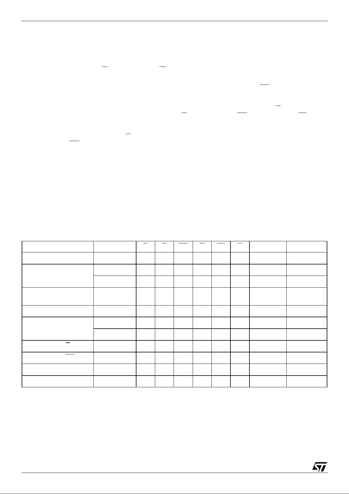
BUS OPERATIONS
Each bus operations that controls the memory is
described in this section, see Tables 4, 5 and 6
Bus Operations, for a summary. The bus operation
is selected through the Burst Configuration Register; the bits in this register are described at the end
of this section.
On Power-up or after a Hardware Reset the memory defaults to Asynchronous Bus Read and Asynchronous Bus W rite, no other b us operation can
be performed until the Burst Control Register has
been configured.
The Electronic Signature, CFI or Status Register
will be r ead in a synchronous mode rega rdless of
the Burst Control Register settings.
Typically glitches of less than 5ns on Chip Enable
or Write Enable are ignored by the memory and do
not affect bus operations.
Asynchronous Bus Operation s
For asynchronous bus operations refer to Table 4
together with the following text.
Asynchronous Bus Read. Asynchronous Bus
Read operations read f rom the memory cells, or
specific registers (Electronic Signature, Status
Register, CFI and Burst Configuration Register) in
the Command Interface. A valid bus ope ration involves setting the desired address on the Address
Inputs, applying a Low signal, V
IL
, to Chip Enable
and Output Enable and keeping Write Enable and
Output Disable High, V
IH
. The Data Inputs/Outputs will output the value, see Figure 9, Asynchronous Bus Read AC Waveforms, and Table 16,
Asynchronous Bus Read AC Characteristics, for
details of when the output becomes valid.
Asynchronous Read is the default read mode
which the device enters on power-up or on return
from Reset/Power-Down.
Asynchronous Latch Controlled Bus Read.
Asynchronous Latch Controlled Bus Read operations read from the memory cells or specific registers in the Command Interface. The address is
latched in the memory before the value i s output
on the data bu s, allowing the address to c hange
during the cycle without affecting the address that
the memory uses.
A valid bus operati on involves s etting the d esired
address on the Address Inputs, setting Chip Enable and Latch Enable Low, V
IL
and keeping Write
Enable High, V
IH
; the address is latched on the rising edge of Latch Enabl e. Once latched, the Address Inputs can change. Set Output Enable Low,
V
IL
, to read the data on the Data Inputs/Outputs;
see Figure 1, Asynchronous Latch Controlled Bus
Read AC Waveforms and Table 17, Asynchronous Latch Controlled Bus Read AC Ch aracteristics for details on when the output becomes valid.
Note that, since the Latch Enable input is transparent when set Low, V
IL
, Asynchronous Bus Read
operations can be performed when the memory is
configured for Asynchronous Latch Enable bus
operations by holding Latch Enable Low, V
IL
throughout the bus operation.
Asynchronous P age R e ad. Asynchronous
Page Read operations are used to read from several addresses within the same memory page.
Each memory page is 4 Double-Words and is addressed by the address inputs A0 and A1.
Data is read internally and stored in the Page Buffer. Valid bus operations are the same as Asynchronous Bus Read operations but with different
timings. The first read operation within the page
has identical timings, subsequent reads within the
same page have much shorter acce ss ti mes. If the
page changes then the normal, longer timings apply again. Page Read does not support Latched
Controlled Read.
See Figure 11, Asynchronous Page Read AC
Waveforms and Table 18, Asynchronous Page
Read AC Characteristics for details on when the
outputs become valid.
Asynchronous Bus Write. Asynchronous Bus
Write operations write to the Command Interface
in order to send commands to the memory or to
latch addresses and input data to program. Bus
Write operations are asynchronous, the clock, K,
is don’t care during Bus Write operations.
A valid Asynchronous Bus W rite operation begins
by setting the desired address on the A ddress Inputs, and setting Chip Enable, Write Enable and
Latch Enable Low, V
IL
, and Output Enable High,
V
IH
, or Output Disable Low, VIL. The Address Inputs are latched by the Command Interface on the
rising edge of Chip Enable or Write Enable, whichever occurs first. Commands and Input Data are
latched on the rising edge of Chip Enable, E
, or
Write Enable, W
, whichever occurs first. Output
Enable must remain High, and Output Disable
Low, during the whole Asynchronous Bus Write
operation.
See Figure 12, Asynchronous Write AC Waveforms, and Table 19, Asynchronous Write and
Latch Controlled Write AC Charact eristics, for details of the timing requirements.
Asynchronous Latch Controlled Bus Write.
Asynchronous Latch Controlled Bus Write operations write to the Command Interface in order to
send commands to the memory or to latch addresses and input data t o program. Bus W rite operations are asynchronous, the c lock, K, is don’t
care during Bus Write operations.
A valid Asynchronous Latch Controlled Bus Write
operation begins by setting the desired address on
M58BW016BT, M58BW016BB, M58BW016D T, M58BW016DB
16/63
the Address Inputs and pulsing Latch Enable Low,
V
IL
. The Address Inputs are latc hed by the Command Interface on the rising edge of Latch Enable,
Write Enable or Chip Enable, whichever occurs
first. Commands and Input Data are latched on the
rising edge of Chip Enable, E
, or Write Enable, W,
whichever occurs first. Output Enable must remain
High, and Output Dis able Low, during the whole
Asynchronous Bus Write operation.
See Figure 13, Asynchronous Latch Controlled
Write AC Waveforms, and Table 19, Asynchronous Write and Latch Controlled Write AC Characteristics, for details of the timing requirements.
Output Disable. The data outputs are high impedance when the Output Enable, G
, is at VIH or
Output Disable, GD
, is at VIL.
Standby. When Chip Enable is High, V
IH
, and the
Program/Erase Controller is id le, the memory enters Standby mode, the power consumption is reduced to the standby level and the Data Inputs/
Outputs pins are placed in the high impedance
state regardless of Output Enable, Write Enable or
Output Disable inputs.
Automatic Low Power. If there is no change in
the state of the bus for a short period of time during
Asynchronous Bus Re ad operations the memory
enters Auto Low Pow er mode where the internal
Supply Current is reduced to the Auto-Standby
Supply Current. The Data Inputs/Outputs will still
output data if a Bus Read operation is in progress.
Automatic Low Power is only available in Asynchronous Read modes.
Power-Down . The memory is in Power-down
when Reset/Power-Down, RP
, is at VIL. The power consumption is reduced to the power-down level and the outputs are high impedance,
independent of the Chip Enable, E
, Output Enable,
G
, Ou t put D i sa b l e, GD , or Wri te Enable, W, inputs.
Electronic Signature. Two codes identifying the
manufacturer and the device can be read from the
memory allowing programming equipment or applications to autom atically mat ch their interface to
the characteristics of the memory. The Electronic
Signature is output by giving the Read Electronic
Signature command. The manufacturer code is
output when all the Address inputs are at V
IL
. The
device code is output when A1 is at V
IH
and all the
other address pins are at V
IL
. See Table 5. Issue
a Read Memory Array command to return to Read
mode.
Table 4. Asynchronous Bus Operations
Note: X = Don’ t Ca re
Bus Operation Step E G GD W RP L A0-A18 DQ0-DQ31
Asynchronous Bus Read
V
IL
V
IL
V
IH
V
IH
V
IH
V
IL
Address Data Output
Asynchronous Latch
Controlled Bus Read
Address Latch
V
IL
V
IH
V
IH
V
IL
V
IH
V
IL
Address High Z
Read
V
IL
V
IL
V
IH
V
IH
V
IH
V
IH
X Data Output
Asynchronous Page
Read
V
IL
V
IL
V
IH
V
IH
V
IH
X Address Data Output
Asynchronous Bus Write
V
IL
V
IH
X
V
IL
V
IH
V
IL
Address Data Input
Asynchronous Latch
Controlled Bus Write
Address Latch
V
IL
V
IL
V
IH
V
IH
V
IH
V
IL
Address High Z
Write
V
IL
V
IH
X
V
IL
V
IH
V
IH
X Data Input
Output Disable, G
V
IL
V
IH
V
IH
V
IH
V
IH
X X High Z
Output Disable, GD
V
IL
V
IL
V
IL
V
IH
V
IH
X X High Z
Standby
V
IH
XXX
V
IH
X X High Z
Reset/Power-Down X X X X
V
IL
X X High Z

17/63
M58BW016BT, M58BW016BB, M58BW016DT, M58BW016DB
Table 5. Asynchronous Read Electronic Signature Operation
Note: 1. x= B or D version of the device.
2. BCR= Burst Configuration Register.
Synchronous Bus Operations
For synchronous bus o perations refer to Table 6
together with the following text.
Synchronous Burs t R ea d. Synchronous Burst
Read operations are used to read from the memory at specific times synchronized to an external reference clock. The burst type , length and latency
can be configured. The different configurations for
Synchronous Burst Read operations are described in the Burst Configuration Register section. Refer to Figures 5 and 6 for examples of
synchronous burst operations.
In continuous burst read, one burst read operation
can access the entire memory sequentially by
keeping the Burst Address Advance B
at VIL for
the appropriate number of clock cycles. At the end
of the memory address space t he burst read restarts from the beginning at address 000000h.
A valid Synchronous Burst Read operation begins
when the Burst Clock is active and Chip Enable
and Latch Enable are Low, V
IL
. The burst start address is latched and loaded into the internal B urst
Address Counter on the valid Burst Clock K edge
(rising or falling depending on the value of M6) or
on the rising edge of Latch Ena ble, whichev er occurs first.
After an initial memory latency time, the memory
outputs data each clock cycl e (or two clo ck cycl e s
depending on the value of M9). The Burst Address
Advance B input controls the memory burst output.
The second burst output is on the nex t cloc k valid
edge after the Burst A ddress Advance B
has been
pulled Low.
Valid Data Ready, R, monitors if the memory burst
boundary is exceeded and the Burst Controller of
the microprocessor needs to insert wait states.
When Valid Data Ready is Low on the active clock
edge, no new data is available and the memory
does not increment the internal address counter at
the active clock edge even if Burst Address Advance, B
, is Low.
Valid Data Ready may be configured (by bit M8 of
Burst Configuration Regist er) to be valid imm ediately at the valid clock edge or one data cycle before the valid clock edge.
Synchronous Burst Read will be suspended if
Burst Address Advance, B
, goes High, VIH.
If Output Enable is at V
IL
and Output Disable is at
V
IH
, the last data is still valid.
If Output Enable, G
, is at VIH or Output Disable,
GD
, is at VIL, but the Burst Address Advance, B, is
at V
IL
the internal Burst Addres s Counter is incre-
mented at each Burst Clock K valid edge.
The Synchronous Burst Read timing diagrams
and AC Characteristics are described in the AC
and DC Parameters section. See Figures 14 , 15,
16 and 17, and Table 20.
Synchronous Burst Read Suspend. During a
Synchronous Burst Read operation it is possible to
suspend the operation, freeing the data bus for
other higher priority devices.
A valid Synchronous Burst Read operation is suspended when b oth Output Enable an d Burst Address Advance are H igh, V
IH
. The Burst Address
Advance going High, V
IH
, stops the burst counter
and the Output Enable going High, V
IH
, inhibits th e
data outputs. The Synchronous Burst Read operation can be resumed by setting Output Enable
Low.
Code Device E G GD W A18-A0 DQ31-DQ0
Manufacturer All
V
IL
V
IL
V
IH
V
IH
00000h 00000020h
Device
M58BW016xT
(1)
V
IL
V
IL
V
IH
V
IH
00001h 00008836h
M58BW016xB
(1)
V
IL
V
IL
V
IH
V
IH
00001h 00008835h
Burst Configuration
Register
V
IL
V
IL
V
IH
V
IH
00005h
BCR
(2)

M58BW016BT, M58BW016BB, M58BW016D T, M58BW016DB
18/63
Table 6. Synchronous Burst Read Bus Operations
Note: 1. X = Don't Care, VIL or VIH.
2. M15 = 0, Bit M15 is in the Burst Configuration Register.
3. T = transition, see M6 in the Burst Configurati on Regist er for detail s on the acti ve edge of K.
Bus Operation Step E G GD RP
K
(3)
L B
A0-A18
DQ0-DQ31
Synchronous Burst
Read
Address Latch
V
IL
V
IH
X
V
IH
T
V
IL
X Address Input
Read
V
IL
V
IL
V
IH
V
IH
T
V
IH
V
IL
Data Output
Read Suspend
V
IL
V
IH
X
V
IH
X
V
IH
V
IH
High Z
Read Resume
V
IL
V
IL
V
IH
V
IH
T
V
IH
V
IL
Data Output
Burst Address Advance
V
IL
V
IH
X
V
IH
T
V
IH
V
IL
High Z
Read Abort, E
V
IH
XX
V
IH
X X X High Z
Read Abort, RP
XXX
V
IL
X X X High Z

19/63
M58BW016BT, M58BW016BB, M58BW016DT, M58BW016DB
Burst Configuration Register
The Burst Configuration Register is used to configure the type of bus access that the memory will
perform.
The Burst Configuration Register is set through
the Command Interface and will retain its information until it is re-configured, the device is reset, or
the device goes into Reset/Power-Down mode.
The Burst Configuration Register bits are described in Table 7. They specify the selection of
the burst length, burst type, burst X and Y latencies and the Read operat ion. Refer to Figures 5
and 6 for examples of sync hronous burst configurations.
Read Select Bit (M15). The Read Select bit,
M15, is used to switch between asynchronous and
synchronous Bus Read operations. When the
Read Select bit is set to ’1’, Bus Read operations
are asynchronous; when the Read Select but is
set to ’0’, Bus Read operations are synchronous.
On reset or power-up the Read Select bit is set
to’1’ for asynchronous accesses.
X-Latency Bits (M14-M11). The X-Latency bits
are used during Synchronous Bus Read operations to set the number of clock cycles between
the address being latched and the first data becoming available. For correct operation the X-Latency bits can only assume the values in Table 7,
Burst Configuration Register. The X -Latency bits
should also be selected in conjunction with Table ,
Burst Performance to ensure valid settings.
Y-Latency Bit (M9). The Y-Latency bit is used
during Synchronous Bus Read operations to set
the number of clock cycles between consecutive
reads. The Y-Latency value depends on both the
X-Latency value and the setting in M9.
When the Y-Latency i s 1 the data changes each
clock cycle; when the Y-Latency is 2 the data
changes every se cond clock cycle. See Tab le 7,
Burst Configuration Register and Table , Burst
Performance, for valid combinations of the Y-Latency, the X-Latency and the Clock frequency.
Valid Data Ready Bit (M8). The Valid Data
Ready bit controls the timing of the Valid Data
Ready output pin, R. When the Valid Data Ready
bit is ’0’ the Valid Data Ready output pin is driven
Low for the active clock edge when invalid data is
output on the bus. When the Valid Data Ready bit
is ’1’ the Valid Data Ready output pin is driven Low
one clock cycle prior to invalid data being output
on the bus.
Burst Type B it (M7). The Burst Type bit is used
to configure the sequence of addresses read as
sequential or interleaved. When the Burst Type bit
is ’0’ the memory outputs from interleaved addresses; when the Burst Type bit is ’1’ the memory
outputs from sequential addresses. See Tables 8,
Burst Type Definition, for the sequence of addresses output from a given starting address in
each mode.
Valid Clock Edge Bit (M6). The Valid Clock
Edge bit, M6, is used to configure the active e dge
of the Clock, K, during Synchronous Burst Read
operations. When the Valid Clock Edge bit is ’0’
the falling edge of the Clock is the active edge;
when the Valid Clock Edge bit is ’1’ the rising edge
of the Clock is active.
Wrap Burst Bit (M3). The burst reads can be
confined inside the 4 or 8 Double-Word boundary
(wrap) or overcome the boundary (no wrap). The
Wrap Burst bit is used t o select between wrap and
no wrap. When the Wrap Burst bit is set to ‘0’ the
burst read wraps; when it is set to ‘1’ the burst read
does not wrap.
Burst Length Bit (M2-M0). The Burst Length bits
set the maximum number of Double-Words that
can be output durin g a Synchronous Burst Read
operation before the address wraps. Burst lengths
of 4 or 8 are available for both the Sequential and
Interleaved burst types, and a continuous burst is
available for the Sequential type.
Table 7, Burst Configuration Register gives the
valid combinations of the Burst Length bits that the
memory accepts; Table 8, Burst Ty pe Definition,
gives the sequence of addresses output from a
given starting address for each length.
If either a Continuous or a No Wrap Burs t Read
has been initiated the device will output data synchronously. Depending on the starting address,
the device activates the Valid Dat a Ready output
to indicate that a delay is necessary before the
data is output. If t he s tarting address is align ed t o
an 8 Double Word boundary, the continuous burst
mode will run without activating the Valid Data
Ready output. If the starting address is not aligned
to an 8 Double Word boundary, Valid Data Ready
is activated to indicate that the device needs an internal delay to read the successive words in the array.
M10, M5 and M4 are reserved for future use.
 Loading...