

8 Mbit (256Kb x32, Burst) Flash Memory
■ SUPPLY VOLTAGE
–VDD= 5V Supply Voltage
–V
– OptionalVPP=12Vforfast Program andErase
■ CONFIGURABLE OPTIONS
– Synchronous or Asynchronous write mode
– Burst Wrap/No-wrap default
– Critical Word X (3 or 4) and Burst Word
■ ACCESS TIME
– Synchronous X-Y-Y-Y Burst Read
– Asynchronous Read: 100ns
■ PROGRAMMING TIME: 10µs typical
■ MEMORY BLOCKS
– 32 equal Main blocks of 256 Kbit
– One Overlay block of 256 Kbit
■ ELECTRONIC SIGNATURE
– Manufacturer Code: 20h
– Device Code: F0h
– Version Code: 0-7h
DESCRIPTION
The M58BF008 is a family of 8 Mbit non-volatile
Flash memories that can be erased electrically at
the blocklevel and programmed in-system. Family
members are configured during product testingfor
a specific Synchronous or Asynchronous Write
mode, a Burst default of Wrap or No-wrap and for
Critical Word X = 3or 4 and Burst WordY = 1 or 2
latency times. The Main memory array matrix allows each of the 32 equal blocks of 256 Kbit to be
erased separately and re-programmed without affecting other blocks. The memory features a
256 Kbit Overlay block having the same address
space asthe firstMain memoryblock. TheOverlay
block provides a secure storage area that is controlled by special Instructions and an external input. A separate supply V
Output signals to be at 3.3Vlevels, while the main
supply VDDis 5V.
= 3.3V Input/Output Supply Voltage
DDQ
Y (1 or 2) latency times
up to 40MHz
allows the Input/
DDQ
BGA
LBGA80 (ZA)
10 x 8 solder balls
Figure 1. Logic Diagram
V
V
DD
DDQVPP
18
A17-A0
CLK
RP
E
G
GD
W
LBA
WR
BAA
M58BF008
V
SS
M58BF008
PRELIMINARY DATA
PQFP80 (D)
32
DQ31-DQ0
V
SSQ
AI02656B
February 2000
This is preliminary information on a new product now in development or undergoing evaluation. Details are subject to change without notice.
1/36
M58BF008
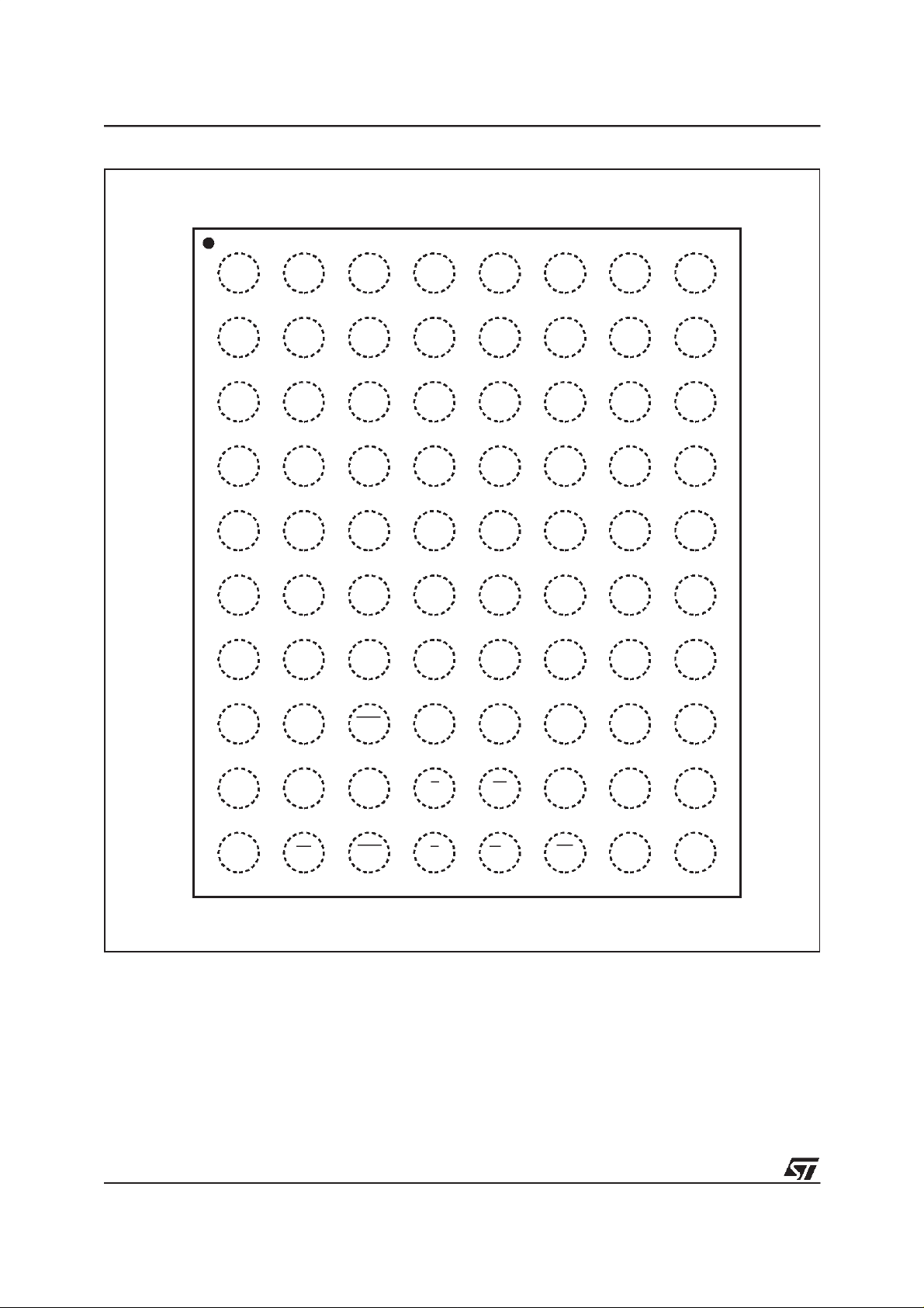
Figure 2. LBGA Connections (Top view through package)
87654321
A16 A9
A14A17B
DQ3DQ4D
G
A12 A10
V
DDQ
V
SSQ
V
DDQ
V
SSQ
A11A13A15A
V
DD
DU
DU DU
DU DU
V
DDQ
V
V
SS
PP
DU
V
V
V
V
DDQ
SSQ
SSQ
DDQ
DQ30
DQ26DQ6DQ8F
A3A4A8
A2A1A6A7
DQ31A5A0DQ0DQ2DQ1C
DQ28
DQ27DQ29DQ5DQ7E
DQ25
DQ24DQ23DQ9DQ10
2/36
H
J
K
RP
BAADQ12DQ11
LBA
V
SS
G
E
DD
W
WR
DQ19DQ201DQ22V
DQ17DQ21DQ18CLKDQ13DQ14
DQ16DUGDDQ15
AI02668
Figure 3. PQFP Connections
GDWRWNCG
NC
M58BF008
SS
DD
E
V
LBA
BAA
V
NC
NC
CLK
RP
DDQ
V
DQ16
DQ17
DQ18
DQ19
V
DDQ
V
SSQ
DQ20
DQ21
DQ22
DQ23
DQ24
DQ25
DQ26
DQ27
V
DDQ
V
SSQ
DQ28
DQ29
DQ30
DQ31
NC
A0
A1
A2
1
12
73
M58BF008 53
32
DQ15
DQ14
DQ13
DQ12
V
SSQ
V
DDQ
DQ11
DQ10
DQ9
DQ8
DQ7
DQ6
DQ5
DQ4
V
SSQ
V
DDQ
DQ3
DQ2
DQ1
DQ0
NC
NC
A17
A16
A3
A4
A5
A6
A7
A8
V
SS
V
PP
V
DD
A9
A10
A11
A12
A13
A14
AI02661
A15
3/36
M58BF008
Table 1. Signal Names
A0-A17 Address Inputs
DQ0-DQ31 Data Input/Output
CLK System Clock
RP Reset/Power-down
E Chip Enable
G Output Enable
GD Output Disable
W Write Enable
LBA Load Burst Address
WR Write/Read
BAA Burst Address Advance
V
DD
V
DDQ
V
PP
V
SS
V
SSQ
NC Not Connected Internally
DU Don’t Use as Internally Connected
Supply Voltage
Supply Voltage for Input/Output
Buffers
Program Supply Voltage
Ground
Input/Output Ground
A Command Interface decodes the Instructions
written to the memory to access or modify the
memory content, to toggle the enable/disable of
read access to the Overlay block, to toggle the
burst Wrap/No-wrap or to toggle the Synchronous
or Asynchronous Read mode. A Program/Erase
Controller (P/E.C.) executes the algorithms taking
care of the timings necessary for program and
erase operations. The P/E.C. also takes care of
verification to unburden the system microprocessor, while a Status Register tracks the status of
each operation.
The following Instructions are executed by the
memory in either Asynchronous or Synchronous
mode.
Access or modify memory content:
- Read Array
- Read or Clear Status Register
- Read Electronic Signature
- Erase Main memory block or Overlay block
- Program Main memory or Overlay memory
- Program Erase Suspend or Resume
Toggle:
– Asynchronous/Synchronous Read
– Overlay Block Read Enable/Disable
– Burst Wrap/No-wrap
The M58BF008 devices are offered in PQFP80
and LBGA80 1.0mm ball pitch packages.
When the VPPsupply is at VSSthis prevents programming and erasure of the memory blocks and,
in addition, it prevents reading of the Overlay
block. When the VPPsupply is at 5V it enables
both in-system program/erase and read access to
the Overlay block. For a limited time and number
of program/erase cycles the VPPsupply may be
raised to 12V to provide fast program and erase
times.
Table 2. Absolute Maximum Ratings
Symbol Parameter Value Unit
T
A Ambient Operating Temperature
T
BIAS
T
STG
V
IO
V
DD,VDDQ
V
PP
Note: 1. Stresses above those listed in the Table”Absolute Maximum Ratings” may cause permanent damage to thedevice.
Temperature Under Bias –40 to 125 °C
Storage Temperature –55 to 150 °C
Input Output Voltage
Supply Voltage –0.6 to 7 V
Program Voltage –0.6 to 13.5 V
(1)
–40 to 125 °C
–0.6 to V
DDQ
+0.6
V
4/36
M58BF008
ORGANISATION
The M58BF008 has a data path width of 32 bit
(Double-Word) and isorganised as a Main memory array of 32 blocks of 256 Kbit plus an Overlay
block of 256 Kbit having the same address space
as the first Main memory block. The memory map
is shown in Table 3.
The memory is addressed by A0-A17 which are
static for Asynchronous or latched for Synchronous operation. Data Input/Output is static or
latched on DQ0-DQ31, these signals output data,
Table 3. Block Addresses
#
31 256 3E000-3FFFF
30 256 3C000-3DFFF
29 256 3A000-3BFFF
28 256 38000-39FFF
27 256 36000-37FFF
26 256 34000-35FFF
25 256 32000-33FFF
24 256 30000-31FFF
23 256 2E000-2FFFF
22 256 2C000-2DFFF
21 256 2A000-2BFFF
20 256 28000-29FFF
19 256 26000-27FFF
18 256 24000-25FFF
17 256 22000-23FFF
16 256 20000-21FFF
15 256 1E000-1FFFF
14 256 1C000-1DFFF
13 256 1A000-1BFFF
12 256 18000-19FFF
11 256 16000-17FFF
10 256 14000-15FFF
9 256 12000-13FFF
8 256 10000-11FFF
7 256 0E000-0FFFF
6 256 0C000-0DFFF
5 256 0A000-0BFFF
4 256 08000-09FFF
3 256 06000-07FFF
2 256 04000-05FFF
1 256 02000-03FFF
0 256 00000-01FFF
Overlay Block 256 00000-01FFF
Size
(Kbit)
Address Range
status orsignatures read from thememory, or they
input data to be programmed or Instruction commands to the Command Interface.
Asynchronous mode
Memorycontrol isprovidedby ChipEnable E, Output Enable G and Write Enable W for read and
write operations.
Synchronous mode
Memorycontrol isprovided byLoad BurstAddress
LBA which loads a read or write address. A Synchronous Single Read or a Synchronous Burst
Read is performed under control of Output Enable
G. Synchronous Write is controlled by Write/Read
Enable WR, Load Burst Address LBA and Write
Enable W. Internal advance of theburst address is
controlled by Burst Address Advance BAA.
SIGNAL DESCRIPTIONS
See Figure 1 and Table 1.
Address Inputs (A0-A17). The address signal
A17 is the MSB and A0 the LSB.
In theAsynchronous mode the addresses must be
stable before Chip Enable E and Write Enable W
go to VIL. They mustremain stable during the read
or write cycle.
In the Synchronous modes, the addresses are
latched by the rising edge of the System Clock
CLK when both Latch Burst Address LBA and
Chip Enable E are at VIL. The addresses are
latched fora read operation if Write/ReadWR is at
VIHor for a write operation when it is at VIL.
Data Input/Output (DQ0-DQ31). The data signal
DQ31 is the MSB and DQ0 the LSB. Commands
are input on DQ0-DQ7.
Data input is a Double-Wordto beprogrammed in
the memory or an Instruction command to the
Command Interface.Data is read from theMain or
Overlay memory blocks, the Status Register orthe
Electronic Signature.
In the Asynchronous mode data is read when the
addresses are stable and Chip EnableE and Output Enable G are at VIL. Commands or address/
data are written when Chip Enable E and Write W
are at VIL.
In the Synchronous mode, after addresses are
latched, data is read on a rising edge of the System Clock CLK when Chip Enable E is at VILand
if Output Enable was at VILon the previous rising
clock edge. Data is written on a rising edge of the
System Clock CLK when Chip EnableE and Write
Enable W are at VIL.
The outputs are high impedance when Chip Enable E or OutputEnable G are atVIH, or whenOutput Disable GD is at VIL. Outputs are also high
impedance when System Reset RP is at VIL.
5/36

M58BF008
System Clock (CLK). All synchronous signals
are input and output relative to the System Clock.
Synchronous input signals must respect the setup and hold times relative to theSystem Clock rising edge.
Reset/Power-down (RP). The Reset/Power-
down RP input provides a hardware reset for the
memory. When Reset/Power-down RP is at V
IL
the memoryis reset and in thePower-down mode.
In this mode the outputs are high impedance and
the current consumption is minimised. When Reset/Power-down RP is at VIHthe memory is in the
normal operating mode. When leaving the Powerdown mode the memory entersthe Asynchronous
Read Array mode.
Reset/Power-down has a weak pull-up resistor to
V
and will assume a high level if not connect-
DDQ
ed.
Chip Enable (E). When the Chip Enable E input
is at VILit activates the memory control logic, input
buffers, decoders and sense amplifiers. When
Chip Enable E is at VIHthe memory is deselected
and the power consumption is reduced to the
standby level.
Output Enable (G). Output EnableG controls the
data output buffers. In the Asynchronous mode
data is output when Output Enable G is at VIL.In
the Synchronous mode, Output Enable G is sampled on the rising edge of the System Clock CLK.
If OutputEnable E is at VILthen valid output data
on DQ0-DQ31 can be read at the next risingedge
of the System Clock CLK.
Output Disable (GD). In the Asynchronous
mode thedata outputsDQ0-DQ31 arehigh impedance when Output Disable GD is at VIL, irrespective of the state of Output Enable G. In
Synchronous mode Output Disable GD is sampled, together with Output Enable G, on the rising
edge of the System Clock CLK. If Output Disable
is at VILthenthe data outputsDQ0-DQ31 arehigh
impedance at the next rising edge of the System
Clock CLK, irrespective of the state of Output Enable G.
Output Disable has a weak pull-up resistor to
V
and willassume a high level if not externally
DDQ
connected.
Write Enable (W). The Write Enable W input
controls the writing of commands or input data. In
the Asynchronous mode commands or data are
written when Chip Enable E and Write Enable W
are at VIL. In the Synchronous mode with Chip Enable E at VIL, input data is sampledif Write Enable
WisatVILon the rising edge of the System Clock
CLK.
Load Burst Address (LBA). In the Asynchronous mode LoadBurst Address LBA isDon’t Care
(but if it falls during an asynchronous read then a
new read cycle is started). In the Synchronous
mode Load BurstAddress LBAenables latching of
the burst starting address forSynchronous read or
write. The address is latchedon the rising edge of
the System Clock CLK if Load Burst Address LBA
is at VIL.
Write/Read (WR). Write/Read WR is used in
Synchronous mode to control write or readoperations. If Load Burst Address LBA is at VILand
Write/Read is at VILthen the rising edge of the
System Clock CLK latches a write address. If
Write/Read is at VIHthen a read address is
latched.
Write/Read has a weak pull-up resistor to V
DDQ
and will assume a high level if not externally connected.
Burst Address Advance (BAA). When Burst
Address Advance BAA is at VIL, the rising edge of
the System Clock CLK advances the burst address. When BurstAddress AdvanceBAA isat V
IH
the advance is suspended.
VDDSupply Voltage. The supply VDDprovides
the power to the internal circuits of the memory.
The VDDsupply voltage is 4.5 to 5.5V.
V
Input/Output Supply Voltage. The Input/
DDQ
Output supply V
provides thepower for the in-
DDQ
put/outputs of the memory, independent from the
supply VDD. The Input/Output supply V
DDQ
may
be connected to the VDDsupply or it can use a
separate supply of 3.0 to 3.6V.
VPPProgram/Erase Supply Voltage. The Program/Erase supply VPPis used for programming
and erase operations. The memory normally executes program and erase operations at the supply
V
voltage levels.
PP1
In a manufacturing environment, programming
may be speeded upby applying ahigher V
PPH
level to the VPPProgram/EraseSupply. Thisis not intended forextended use. The V
supply may be
PPH
applied for atotal of 80 hours maximumand during
program anderase for a maximum of 1000 cycles.
Stressing the device beyond these limits could
damage the device.
When VPPProgram/Erase supply is at VSSall
blocks are protected from programming or erase.
Leaving VPPfloating is equivalent to connecting it
to VSSdue to an internal pull-down circuit.
Ground (VSSand V
). The Ground VSSis t he
SSQ
reference for the internal supply voltage VDD.The
Ground V
supply V
is the reference for the Input/Output
SSQ
.
DDQ
6/36
M58BF008
DEVICE OPERATIONS
See Table 4 for Asynchronous or Synchronous
Bus Operations.
In theAsynchronous modethe memoryis selected
with Chip Enable E Low. The data outputs are enabled by Output Enable G Low or disabled by Output Disable GD Low. Datais input byWrite Enable
W Low.
In the Synchronous mode the memory latches addresses and data (input or output) on the rising
edge of the System Clock CLK. Burst address
latching is enabled by Load Burst Address LBA
Low with Write/Read WR Low for a write cycle or
High for a read cycle.
Data outputs are enabled for reading on the rising
edge of the System Clock CLK when Output Enable G is low. Data is input on the rising edge of
the System Clock CLK when Write Enable W is
Low.
power-down mode when Reset/Power-Down RP
is Low.
Read. Read operations are used to output the
contents of the memory, the Electronic Signature
or the Status Register. The data read depends on
the previous Instruction given to the memory.
Read operations can be Asynchronous or Synchronous, witha single or burst read.On power-up
the device is in Asynchronous read mode, the Instruction Asynchronous/Synchronous Read Toggle ART can be used to enter the Synchronous
read mode.
– Asynchronous Read. To read a data Double-
Wordin Asynchronousmode the address inputs
must be stable and Chip Enable E must be Low
during theread cycle. Output Enable Gmust be
Low and Output Disable GD High. The Load
Burst Address LBA is Don’t Care, but its falling
edge will start a new read cycle.
The memory is deselected and in standby mode
when Chip Enable E is High, and it is reset or in
Table 4. Bus Operations
Operation RP CLK E LBA WR W GD G DQ0-DQ31
Asynchronous Read
Asynchronous Write
Synchronous Read
Synchronous Write Address for
Read
Synchronous Write Address for
Command
Synchronous Data Write
Output Disabled by G
Output Disabled by GD
Standby
Reset / Power-down
Note: 1. See Device Operations, Instructions and Commands, sections for more details.
2. X=V
or V
IL
IH.
(1,2)
V
IH
V
IH
V
IH
V
IH
V
IH
V
IH
V
IH
V
IH
V
IH
V
IL
V
X
V
X
V
V
V
V
V
X
V
X
V
X
XX
IL
XX
IL
V
IL
V
IL
V
IL
V
IL
IL
IL
IH
V
IH
IL
IL
IH
IH
V
IH
V
IL
V
IH
XXX
XXX
XXXXX Hi-Z
XXXXXXX Hi-Z
V
V
V
IH
IL
X
X
IH
V
IH
V
IH
V
IH
XVIHV
V
V
IL
IH
V
IH
V
IL
V
V
V
V
V
V
IL
IH
IL
IH
IH
IH
IH
Data Output
Data Input
Data Output
Data Input
Hi-Z
X Hi-Z
X
X
Table 5. Read Electronic Signature
Code RP E G W A0 A1 A2-A17 DQ0-DQ31
Manufacturer
Device
Version
Note: ”x” = version level. The first version is ”0” and it can have a value up to ”7”.
V
IH
V
IH
V
IH
V
IL
V
IL
V
IL
V
IL
V
IL
V
IL
V
IH
V
IH
V
IH
V
IL
V
IH
V
IL
V
IL
V
IL
V
IH
Don’t Care 00000020h
Don’t Care 000000F0h
Don’t Care 0000000xh
7/36

M58BF008
– Synchronous Single Read. To read a single
data Double-Word in Synchronous mode Chip
Enable E must be Low. Load Burst Address
LBA must be Low for one System ClockCLK rising edgewith Write/Read WRHigh. This latches
the read address, after which the address bus
inputs are Don’t Care. The Output Enable G is
Low for a single System Clock CLK cycle. The
Double-Word of valid data is output on the next
System Clock CLK rising edge.
– Synchronous Burst Read. To read a burst of
four Double-Words in Synchronous mode Chip
Enable /E must be Low. Load Burst Address
LBA must be Low for one System ClockCLK rising edgewith Write/Read WRHigh. This latches
the first address of the burst sequence, after
which the address bus inputs are Don’t Care.
The Output Enable G is driven Low before the
burst output sequence. Four Double-Words of
data are output on the subsequent System
Clock CLK rising edges if Burst Address Advance BAA is maintainedLow. The address advance for synchronous burst read is suspended
if Burst Address Advance BAA goes High and
the output data remains constant. The data bus
will go high impedanceon the rising edge ofthe
System Clock CLK after Output Enable G goes
High.
The burst timing depends on the device configuration for theCritical Word X and BurstWord Y
latency times and the choiceof wrap orno-wrap
for burst addresses. The operation burst wrap is
shown in Table 13. The wrap sequence uses
only the address bits A0 and A1 and does not
repeat after the last Double-Wordhas been output.
Read Overlay Block. The Overlay block can be
read, as for a Main block, after it has been enabled. To enable the Overlay block the Overlay
Block Enable bit OBEB and the OverlayBlock Status bit OBS in the Status Register must be set to
’1’- see Table 9.
The Overlay Block Enable bit OBEB can be set to
’1’in three ways - see Table 10:
– By Toggling the Reset/Power-Down signal RP
with the VPPProgram/Erase supply in the range
V
PP1
or V
PPH.VPP
out of range will reset the
OBEB bit to ’0’.
– By a leaving power-on reset with VPPProgram/
Erase supplyin the rangeV
PP1
orV
PPH.VPP
out
of range will reset the OBEB bit to ’0’.
– By giving the Overlay Block Enable/Disable for
Read Instruction OBT.
The Overlay Block Status bit OBS monitors the
VPPProgram/Erase supply and will be set to ’1’
when in the range V
PP1
or V
. The Overlay
PPH
block is enabled with OBEB at ’1’ but will not be
read unless OBS status bit is also at ’1’. If it is not
then a read operation will read the contents of the
Main block at the same address.
When the Overlay block is enabled for reading,
only this one block of 256 Kbit is accesible and
none of the other Main blocks may be accessed,
the address signals A13-A17 are Don’tCare.
Read Electronic Signature. The memory contains three Electronic Signature codes identifying
the manufacturer, device and version, which can
be read after giving the Instruction RSIG. The
manufacturer code 00000020h is read when the
address inputs A0 and A1 are at VIL. The device
code 000000F0his read when A0 isat VIHand A1
is at VIL. The version code 0000000xh is read
when A0 is at VILand A1 is at VIH. The codes are
read on DQ0-DQ31,all other address signalinputs
are Don’t Care. See Table 5.
Write. Write operations are used to give commands tothe memory that latch input data and addresses to program or block addresses to erase.
– Asynchronous Write. To write data in the
Asynchronous mode the address inputs must
be stable and Chip Enable E must be Low during thewrite cycle. WriteW mustbe Low andinput data valid on the rising edge is Write W.
– Synchronous Write. To write input data in
Synchronous mode Chip Enable E must be
Low. Load Burst Address LBA must be Low for
one System Clock CLK rising edge with Write/
Read WR Low. This latches the write address,
after which the address bus inputs are Don’t
Care. WhenWrite EnableW isLow input datais
latched on the next System Clock CLK rising
edge.
Output Disable. The data outputs are high impedance when the Output Enable G is High or
when the Output Disable GD is Low, independent
of the level on Output Enable G.
Standby. The memory is in standby when the P/
E.C. is not running, the memory is in read mode
and Chip Enable E is High. The power consumption is reducedto the standby level and the outputs
are high impedance, independent of the Output
Enable G or Write Enable W inputs.
If Chip Enable goes High during a program or
erase operation the device enters the standby
mode when the internal algorithm has finished.
Reset/Power-down. During power-down all internal circuits are switched off, the memory is deselected and the outputs arehigh impedance. The
memoryis inPower-down mode whenReset/Power-down RP isLow. The power consumption is reduced to thepower-down level,independent of the
Chip Enable E, Load Burst Address LBA, Output
Enable G or Write Enable W inputs.
If Reset/Power-down RP is pulled Low during a
program or erase operation thisis aborted and the
memory content is no longer valid.
8/36
M58BF008
INSTRUCTIONS AND COMMANDS
The Instructions are listed in Tables 6 and 7. They
may be broadly divided into two types, those that
access or modify the memory content and those
that toggle a mode or function.
The Instructionsthat access ormodify the memory
content include:
– Read Memory Array (RD)
– Read Status Register (RSR) and Clear Status
Register (CLRS)
– Read Electronic Signature (RSIG)
– Erase (EE) and OverlayBlock Erase (OBEE)
– Program (PG) and Overlay Block Program (OB-
PG)
– Program or Erase Suspend (PES) and Program
or Erase Resume (PER)
The Instructions that toggle a mode or function in-
clude:
– Asynchronous/Synchronous Read mode Tog-
gle (ART)
– Wrap/No-wrap Burst mode Toggle (WBT)
– Overlay Block Enable/Disable function Toggle
(OBT)
Instructions are written, in one or more write cy-
cles, to the memory Command Interface (C.I.) for
decoding. The Command Interface is reset to
Read Memory Array at power-up, when exiting
from power-down. Any invalid sequence of commands will also reset the Command Interface to
Read Memory Array.
A Program/Erase Controller (P/E.C.) handles all
the timing and verifies the correct execution of the
Program or Erase instructions. The P/E.C. has a
Status Register which monitors the operations and
which may be read at any time during program or
erase. The Status Register bits indicate the operation and exit status of the internal algorithms.
The VPPProgram and Erase Supply Voltage must
be withinthe range V
PP1
orV
for programming
PPH
or erasure. If VPPout of range, the program or
erase algorithms do not start and Status Register
bit VPPStatus V
will be set to ’1’.
PPS
Table 6. Commands
Code Command
02h Overlay Block Erase Set-up
04h Overlay Block Program Set-up
06h
0Dh Overlay Block Erase Confirm
20h Erase Set-up
30h Wrap/No-wrap Burst Toggle
40h Program Set-up
50h Clear Status Register
60h
70h Read Status Register
90h Read Electronic Signature
B0h Program/Erase Suspend
D0h
FFh Read Memory Array
Overlay Block Read Enable/
Disable
Asynchronous/Synchronous
Read Toggle
Program/Erase Resume or
Erase Confirm
9/36
M58BF008
Table 7. Instructions
Mne-
monic
RD
RSR
CLRS
RSIG
EE Erase 2 Write 00000h 20h Write Block Address D0h
Instruction Cycles
Read Memory
Array
Read Status
Register
Clear Status
Register
Read Electronic
Signature
Operation Address Data Operation Address. Data
1+ Write 00000h FFh
1+ Write 00000h 70h Read X
1 Write 00000h 50h
1+++ Write 00000h 90h Read
1st Cycle 2nd Cycle
Read
Read Address Data Output
Signature
Address
Status
Register
Electronic
Signature
OBEE
PG Program 2 Write 00000h 40h Write
OBPG
PES
PER
ART
WBT
OBT
Read Memory Array (RD). The Read Memory
Array instruction consists of one write cycle giving
the command FFh atthe address 00000h. Subsequent read operations will read the addressed location and output the memory data. The data can
be read from the Main memory Array or the Overlay memory block if it is enabled.
Read Status Register (RSR). The Read Status
Register instructionconsists ofone write cycle giving thecommand 70h attheaddress 00000h.Subsequent read operations will output the Status
Register contents. See Table 8 for an explanation
of the Status Register bits. TheStatus Register indicates when a program or Erase operation is
complete and its success or failure. The Status
Register also indicates if the Overlay block is accessible for reading. The Read Status Register instruction may be given at anytime, including while
Overlay Block
Erase
Overlay Block
Program
Program/Erase
Suspend
Program/Erase
Resume
Asynch/Synch
Read Toggle
Wrap//No-wrap
Burst Toggle
Overlay Block
Read En/Dis
Toggle
2 Write 00000h 02h Write
2 Write 00000h 04h Write
1 Write 00000h B0h
1 Write 00000h D0h
1 Write 00000h 60h
1 Write 00000h 30h
1+ Write 00000h 06h Read Read Address Data Output
Clear Status Register (CLRS). The Clear Status
Register instructionconsists of onewrite cycle giving the command 50h at the address 00000h.The
Clear Status Register command clears the bits 3,
4 and 5 of the Status Registerif theyhavebeen set
to ’1’ by the P/E.C. operation. The Clear Status
Register command should be given after an error
has been detected and before any new operation
is attempted. A Read Memory Array command
should also be given beforedata can beread from
the memory array.
Read Electronic Signature (RSIG). The Read
Electronic Signature instruction consists of a first
write cycle giving the command90h atthe address
00000h. This is followed by three read operations
at addresses xxxx0h, xxxx1h and xxxx2h which
output the manufacturer, device and version
codes respectively.
a program or erase operation in progress.
Overlay Block
Address
Program
Address
Overlay Block
Program
Address
0Dh
Data Input
Data Input
10/36
Table 8. Status Register Bits
Mne-
monic
P/ECS 7 P/E.C. Status
PESS 6
ES 5 Erase Status
Bit Name
Program/Erase
Suspend Status
M58BF008
Logic
Level
’1’ Ready
’0’ Busy
‘1’ Suspend On Program/Erase Suspend instruction both
‘0’
’1’ Erase Error or
’0’ Erase Success
Definition Note
Indicates the P/E.C. status, check during
Program or Erase
P/ECS and PESS bits are set to ‘1’.
In Progress or
Completed
Erase Suspend
Either ES bit or PS bit is set to ‘1’.
PESS and either ES or PS bits remain at ‘1’
until Erase Resume instruction is given.
ES bit is set to ‘1’ if either PESS instruction is
given or Erase operation fails. If ES bit is ‘1’,
check PESS bit.
’1’ Program Error or
PS 4 Program Status
V
VPPS 3
Reserved 2
OBEB 1
OBS 0
Status
PP
Overlay Block
Enable Bit
Overlay Block
Status
Program Suspend
’0’ Program Success
V
’1’
’0’
’1’ Enabled
’0’ Disabled
’1’ Activated
’0’ Not Activated
PP
V
PP
Erase (EE). The Erase instruction consists oftwo
write cycles, the first is the eraseset-up command
20h at theaddress 00000h. Thisis followed by the
Erase Confirm command D0h written to an address within the block to be erased. If the second
is not the Erase Confirm command the Status
Register bits 4 and 5 are set to ’1’and the instruction aborts. While erasing is in progress only the
Read Status Registerand Erase Suspend instructions are valid.
Blocks are erased one at a time. An erase operation sets all bits in a block to ’1’. The erase algorithm automatically programs all bits to ’0’ before
erasing the block to all ’1’s.
Read operations output the Status Register after
the erase operation has started. The Status Register bit 7 is ’0’ whilethe erase is in progress andis
set to’1’when it is completed.After completionthe
Status Register bit 5 is set to ’1’ if there has been
an erase failure.
Erasure should not be attempted when the V
PP
Program/Erase Supply Voltage is out of the range
V
PP1
or V
as the results will be uncertain. The
PPH
PS bit is set to ‘1’ if either PESS instruction is
given or Program operation fails.If PSbit is ‘1’,
check PESS bit.
Invalid VPPS bit is set to ‘1’ if initially VPPis not V
OK
nor V
are executed.
OBEB bit is set to ‘1’ when OverlayBlock is
Enabled.
OBS bit is set to ‘1’ when OBEB is ‘1’ and V
is in the range V
, when Program or Erase Instruction
PP1
PP1
or V
PPH
.
Status Register bit 3 is set to’1’ if VPPis not within
the allowedranges whenerasing is attempted or if
it falls out of the ranges during erase execution.
The erase operation aborts if VPPdrops out of the
allowed range or if Reset/Power-down RP falls to
VIL. As data integrity cannot be guaranteed when
the erase operation is aborted, the erase must be
repeated.
A Clear Status Register instruction must be given
to clear the Status Register bits.
Overlay Block Erase (OBEE). The Overlay
Block Erase instruction consists of two write cycles, the first is the Overlay block erase set-up
command 02h at the address 00000h. This is followed by the Overlay Block Erase Confirm command 0Dh written to an address withinthe Overlay
block. If the secondis not the Overlay Block Erase
Confirm command the Status Register bit 5 is set
to ’1’ and theinstruction aborts. While erasing is in
progress only theRead Status Register instruction
is valid.
The operation is executed as described for the
Erase (EE) instruction of the Main memory array.
A Clear Status Register instruction must be given
to clear the Status Register bits.
PPH
PP
11/36
 Loading...