

SGS Thomson Microelectronics M74HC137M1R, M74HC137C1R, M74HC137B1R, M74HC137, M54HC137F1R Datasheet
3 TO8 LINE DECODER/LATCH (INVERTING)
.HIGH SPEED
tPD= 11 ns(TYP.) AT VCC=5V
.LOWPOWER DISSIPATION
ICC=4µA(MAX.) AT TA=25 °C
.HIGH NOISE IMMUNITY
V
NIH=VNIL
=28%VCC(MIN.)
.OUTPUT DRIVE CAPABILITY
10 LSTTLLOADS
.SYMMETRICALOUTPUT IMPEDANCE
IOH =IOL= 4 mA(MIN.)
.BALANCEDPROPAGATION DELAYS
t
PLH=tPHL
.WIDE OPERATINGVOLTAGE RANGE
VCC(OPR)= 2 V TO6 V
.PIN ANDFUNCTION COMPATIBLE
WITH 54/74LS137
DESCRIPTION
The M54/74HC137 i sahigh speedCMOS 3TO 8LINE
DECODER/LATCH (INVERTING)fabricated in silicon
gate C2MOS technology. It has the same high speed
performance ofLSTTLcombined withtrueCMOSlow
power consumption. This device is a 3 to 8line d ecoder
withlatches on thethree address inputs. WhenGLgoes
from lowtohigh, theaddress present attheselectinputs
(A,BandC)isstoredinthelatches.AslongasGLremains high noaddress changes will berecognized. Output enable pins G1 and G2, control the state of the
outputs independently of the select or latch-enable inputs. All the outputs are high unless G1is high and G2
is low. The HC137is idea lly suited for the implemen tation of glitch-free decoders in stored-address applications in bus oriented systems. All inputs are equipped
withprotection circuitsagainst staticdischarge andtransient excess voltage.
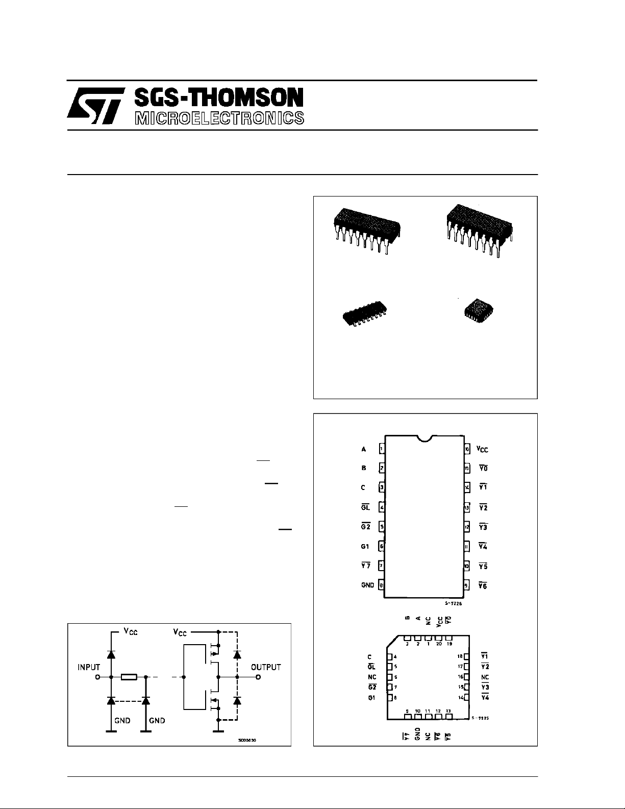
M54HC137
M74HC137
B1R
(PlasticPackage)
M1R
(MicroPackage)
ORDER CODES :
M54HC 137F1R M74H C137M1R
M74HC 137B1R M74HC1 37C1R
PIN CONNECTIONS (top view)
F1R
(CeramicPackage)
C1R
(Chip Carrier)
INPUT AND OUTPUT EQUIVALENT CIRCUIT
February 1993
NC =
No Internal
Connection
1/11
M54/M74HC137
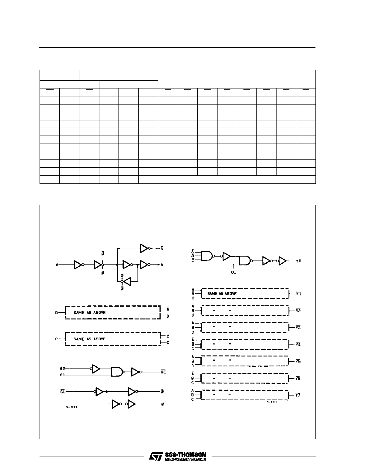
TRUTH TABLE
INPUTS
ENABLE SELECT
GL G1 G2 C B A Y0 Y1 Y2 Y3 Y4 Y5 Y6 Y7
XXHXXXHHHHHHHH
XLXXXXHHHHHHHH
LHL L L LLHHHHHHH
LHL L LHHLHHHHHH
LHL LHLHHLHHHHH
LHL LHHHHHLHHHH
LHLHL LHHHHLHHH
LHLHLHHHHHHLHH
LHLHHLHHHHHHLH
LHLHHHHHHHHHHL
H H L X X X Outputs corresponding to stored address L: all others H
OUTPUTS
LOGI C DIAG RAM
2/11
PIN DESCRIPTION
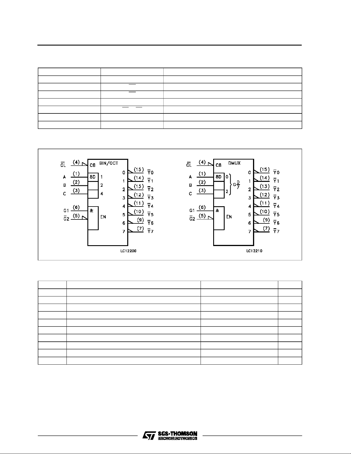
PIN No SYMBOL NAME AND FUNCTION
1, 2, 3 A to C Data Inputs
4 GL Latch Enable Input (Active LOW)
5 G2 Data Enable Input (Active LOW)
6 G1 Data Enable Input (Active HIGH)
15, 14, 13, 12, 11, 10, 9, 7 Y0 to Y7 Multiplexer Outputs
8 GND Ground (0V)
16 V
CC
Positive Supply Voltage
IEC LOGIC SYMBOLS
M54/M74HC137
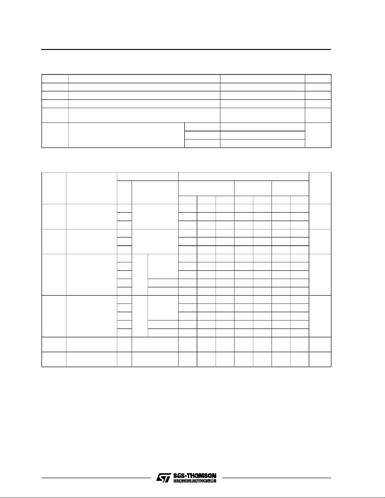
ABSOLU TE M AXI MU M R AT INGS
Symbol Parameter Value Unit
V
CC
V
V
O
I
IK
I
OK
I
O
I
or I
CC
P
D
T
stg
T
AbsoluteMaximumRatingsarethosevaluesbeyond whichdamagetothedevicemayoccur.Functional operationunder theseconditionisnotimplied.
(*)500 mW:≅ 65oC derateto 300 mWby 10mW/oC: 65oCto85oC
Supply Voltage -0.5 to +7 V
DC Input Voltage -0.5 to VCC+ 0.5 V
I
DC Output Voltage -0.5 to VCC+ 0.5 V
DC Input Diode Current ± 20 mA
DC OutputDiode Current ± 20 mA
DC Output Source Sink Current Per Output Pin ± 25 mA
DC VCCor Ground Current ± 50 mA
GND
Power Dissipation 500 (*) mW
Storage Temperature -65 to +150
Lead Temperature (10 sec) 300
L
o
C
o
C
3/11
M54/M74HC137
RECO MM ENDED OPERATI N G CO NDITI O NS
Symbol Parameter Value Unit
V
V
V
T
t
r,tf
DC SPECIFICATIO NS
Symbol Parameter
V
IH
V
V
OH
V
OL
I
I
CC
Supply Voltage 2 to 6 V
CC
Input Voltage 0 to V
I
Output Voltage 0 to V
O
Operating Temperature: M54HC Series
op
M74HC Series
CC
CC
-55 to +125
-40 to +85
Input Rise and Fall Time VCC= 2 V 0 to 1000 ns
V
= 4.5 V 0 to 500
CC
V
= 6 V 0 to 400
CC
Test Conditions Value
V
(V)
CC
=25oC
T
A
54HC and 74HC
-40 to 85oC
74HC
-55 to 125oC
Min. Typ. Max. Min. Max. Min. Max.
High Level Input
Voltage
2.0 1.5 1.5 1.5
4.5 3.15 3.15 3.15
6.0 4.2 4.2 4.2
Low Level Input
IL
Voltage
2.0 0.5 0.5 0.5
4.5 1.35 1.35 1.35
6.0 1.8 1.8 1.8
High Level
Output Voltage
Low Level Output
Voltage
Input Leakage
I
Current
Quiescent Supply
2.0
V
=
I
4.5 4.4 4.5 4.4 4.4
6.0 5.9 6.0 5.9 5.9
4.5 I
6.0 I
2.0
4.5 0.0 0.1 0.1 0.1
6.0 0.0 0.1 0.1 0.1
4.5 I
6.0 I
6.0
IO=-20 µA
V
IH
or
V
IL
=-4.0 mA 4.18 4.31 4.13 4.10
O
=-5.2 mA 5.68 5.8 5.63 5.60
O
V
=
I
IO=20µA
V
IH
or
V
IL
= 4.0 mA 0.17 0.26 0.33 0.40
O
= 5.2 mA 0.18 0.26 0.33 0.40
O
VI=VCCor GND ±0.1 ±1 ±1 µA
1.9 2.0 1.9 1.9
0.0 0.1 0.1 0.1
6.0 VI=VCCor GND 2 20 40 µA
Current
54HC
V
V
o
C
o
C
Unit
V
V
V
V
4/11
 Loading...