

FEATURES
■ 2 DIGIT LED DRIVER (14 segments)
■ CURRENT GENERATOR OUTPUTS (no
registor required)
■ CONTINUOU BRIGHTNESS CONTROL
■ SERIAL DATA INPUT
■ DATA ENABLE
■ WIDE SUPPLY VOLTAGE OPERATION
■ TLL COMPATIBILITY
■ APPLICATION EXAMPLES
■ MICROPROCESSOR DISPLAYS
■ INDUSTRIAL CONTROL INDICATOR
■ RELAY DRIVER
■ INSTRUMENTATI ON READ O U TS
DESCRIPTION
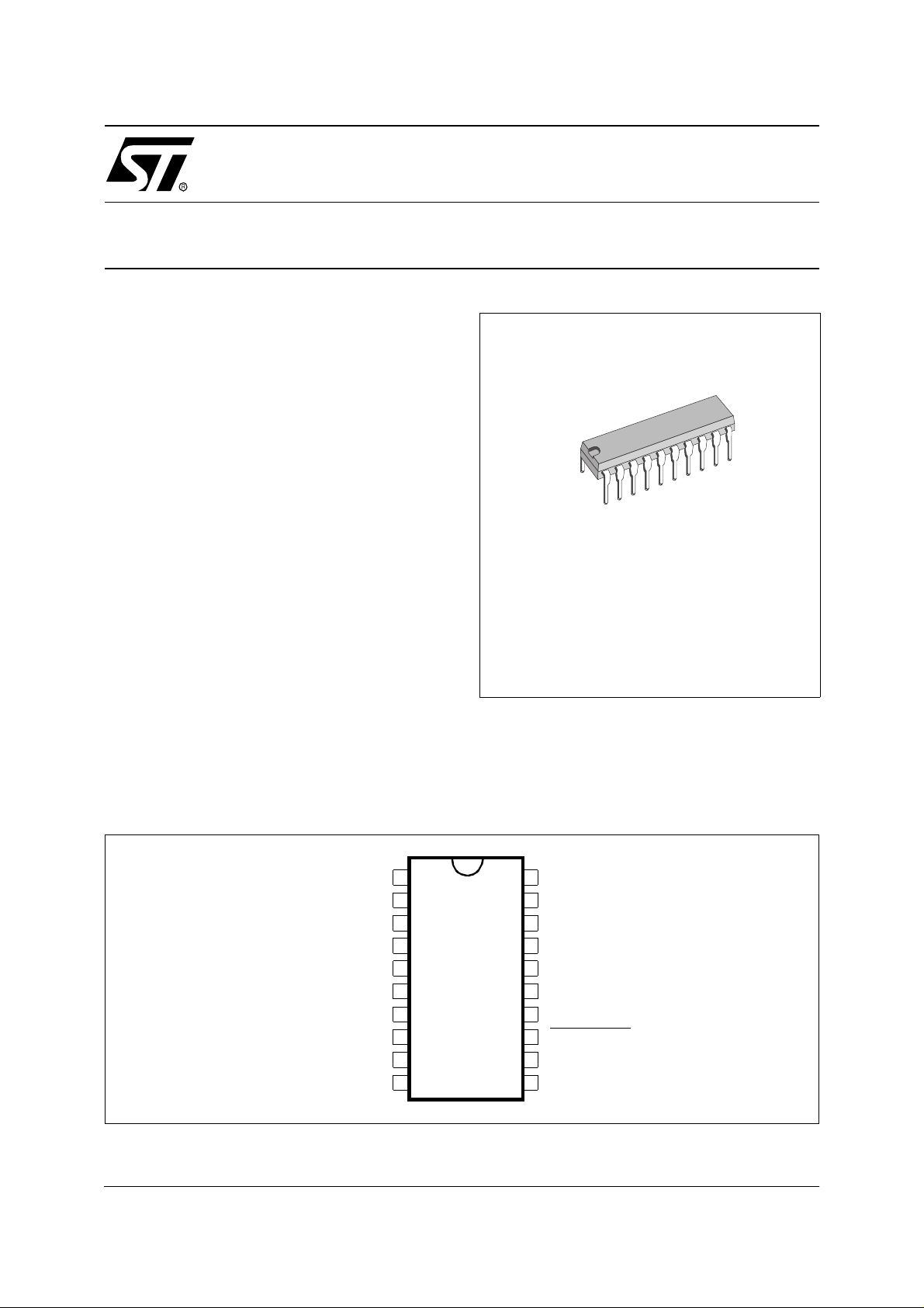
The M5481 is a monolithic MOS integrated circuit
produced with a N-channel silicon gate techn ology. It uses the M54 50 die packaged in a 20-pin
plastic package copper frame, making it ideal for a
1-digit display. A single pin controls the LE D display brightness by setting a reference current
through a variable resistor connected either to
V
DD
or to a separate supply of 13.2V maximum.
The M5481 is a pin-to-pin replacement of the NS
MM 5481.
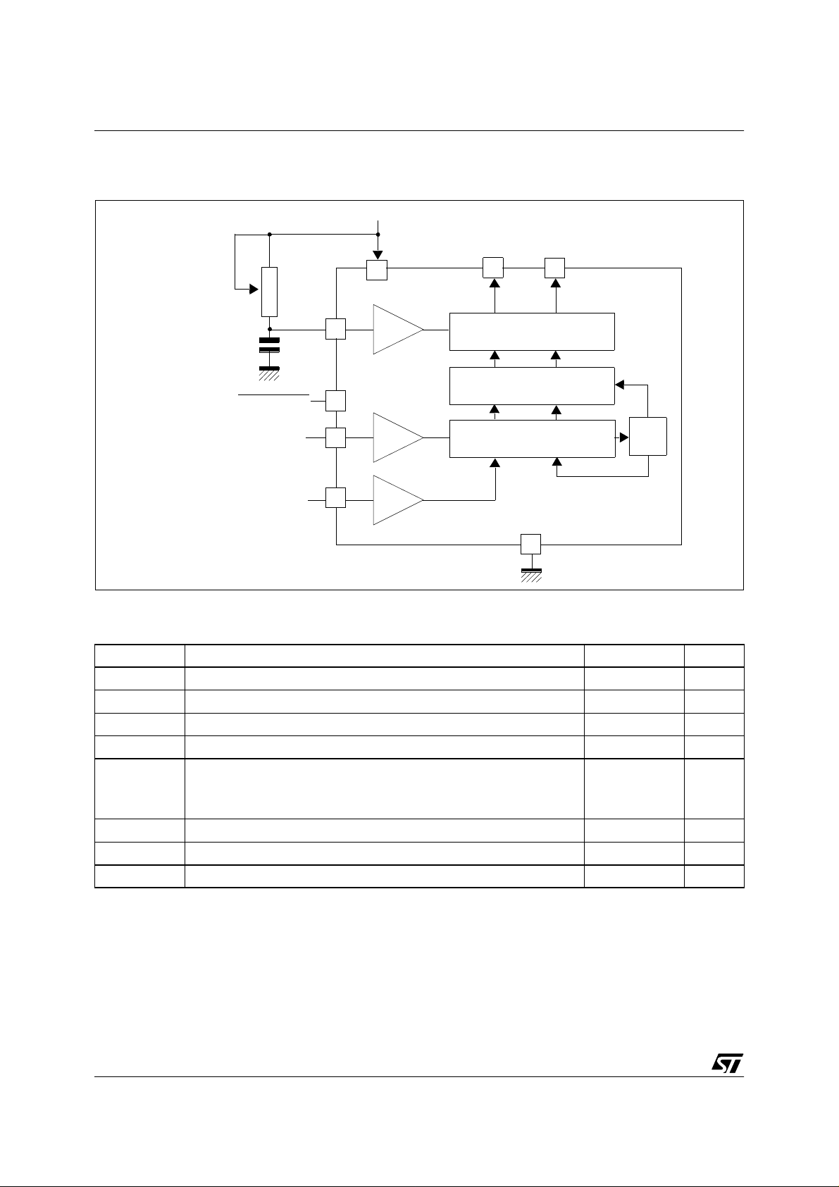
PIN CONNECTIONS
M5481
LED DISPLAY DRIVER
DIP20
(Plastic package)
ORDER CODE: M54 81 B7
Output Bit 8
Output Bit 7
Output Bit 6
Output Bit 5
Output Bit 4
Output Bit 3
Output Bit 2
Output Bit 1
Brightness Control
V
DD
1
2
3
4
5
6
7
8
9
10
20
19
18
17
16
15
14
13
12
11
Output Bit 9
Output Bit 9
Output Bit 9
Output Bit 9
Output Bit 9
V
SS
Output Bit 9
Data Enable
Data In
Clock
Version 4.1
April 2000 1/8
1
M5481
1 - BLOC DIAGRAM
Figure 1.
Brightness
Control
100kΩ
V
10
DD
Output
Bit 14
14
Output
Bit 1
8
9
35 Output Buffers
1nF
Load
Data Enable
Serial Data
Clock
13
12
11
35 Latches
35-Bit Shift Register
Reset
15
2 - ABSOLUTE MAXIMUM RATINGS
Symbol Parameter Value Unit
V
DD
Vi Input Voltage -0.3 to 15 V
Vo(off) Off-state Output Voltage 15 V
Io Output Sink Current 40 mA
Supply Voltage -0.3 to 15 V
Total package power Dissipation
P
tot
T
j
T
oper
T
stg
Stresses exceed ing those list ed under “Ab solute Max imum Rating s” may caus e permanen t damage to the device a nd
affect its reliability.
2/8
Junction Temperatu re 150 °C
Operating Temperature Range -25, +85 °C
Staorage Temperature Range -65, +150 °C
at 25°C
t 85°C
1.5
800
W
mW
2
3 - STATIC ELECTRICAL CHARACTERISTICS
(T
within operational range, VDD=4.75V to 13.2V, VSS=0V, unless otherwise specified)
amb
Symbol Parameter Test Conditions Min Typ Max Unit
V
DD
Idd Supply Current V
Supply Voltage 4.5 13.2 V
=13.2V 7 mA
DD
M5481
Input Voltages
Vi
IB Brightness Input Current (Note 2) 0 0.75 mA
VB Brightness Input Voltage (pin9)
Vo(off) Off-state Output Voltage 13.2 V
Io
fclock
Io Output Matching (Note 1)
Note 1 Output matching is calculated as the percent variation from Imax+Imin/2
Note 2 With a fixed resistor on the brightness input some variation in brightness will occur from one device to another.
Note 3 Absolute maximum for each output should be limited to 40mA.
Note 4 the Vo voltage should be regulated by the user.
Logical “0” Level
Logical “1” Level
Output Sink Current (Note 3)
Segment OFF
Segment ON
Input Clock Frequency 0 0.5 MHz
+10µA Input Bias
4.75≤V
V
DD
Input Curren=750µA
T
amb
Vo=3V
Vo=1V (Note 4)
Brightness In.=0µA
Brightness In.=100µA
Brightness In.=750µA
DD
>5.25
=25°C
≤5.25
-0.3
2.2
V
-
DD
2
3 4.3 V
0
2
12
2.7
15
0.8
V
DD
V
DD
10
10
4
25
±20 %
V
V
V
µA
µA
mA
mA
4 - FUNCTIONAL DESCRIPTION
The M5481 uses the M5450 die which is packaged
to operate 2-digit alphanumeric displays with minimal interface with the display and the data source.
Serial data transfer from the data source to the display driver is accom plished with 2 signals, serial
data and clock. using a format of a leadi ng “1” followed by the 35 data bits allows data transfer without an additional load signal.
The 35 data bits are latched after the 36th bit is
complete, thus providing non-multiplexed, direct
drive to the display. Outputs change only if the serial data bits differ from the previous time. Display
brightness is determined by control of the output
current for LED displays. A 1nF capacitor should
be connected to brightness c ontrol (pin 9) to prevent possible oscillations.
A bloc diagram is shown on F igure 1. The output
current is typically 20 times g reater than the current into pin 9, which is set by an external variable
resistor.
The latter is an internal limiting resistor of 400Ω
nominal value.
Figure 2 shows the input data format. A start bit of
logical “1” precedes the 35 bits of data. At the 36th
clock a LOAD is generated synchronously with the
high state of the clock, which l oads the 35 bits of
the shift registers into the latches.
3/8
 Loading...