

SGS Thomson Microelectronics M5480 Datasheet
.
3 1/2 DIGIT LED DRIV ER (23 segment s)
.
CURRENT GENERATOR OUTPUTS (no resistors required)
.
CONTINUOUS BRIGHTNESS CONTROL
.
SERIAL DATA INPUT
.
NO LOAD SIGNAL REQUIRED
.
WIDE SUPPLY VOLTAGE OPERA TION
.
TTL CO MPAT IB ILI TY
Applications examples
.
MICROPROCESSOR DISPLAYS
.
INDUSTRIAL CONTROL INDICATION
.
RELAY DRIVER
.
INSTRUMENTATION READOUTS
M5480
LED DISPLAY DRIVER
DESCRIPTION
The M5480 is a monolithic MOS integrated circuit
produced with a N-channel silicon gate technology .
It utilizes the M5451 die packaged in a 28-pin
plas-tic package making it ideal for a 3
dispaly . A single pin controls the LED d ispaly brightness by setting a reference current through a variable resistor connected either to V
separate supply of 13.2V maximum.
The M5480 is a pin-to-pin replacement of the NS
MM 5480.
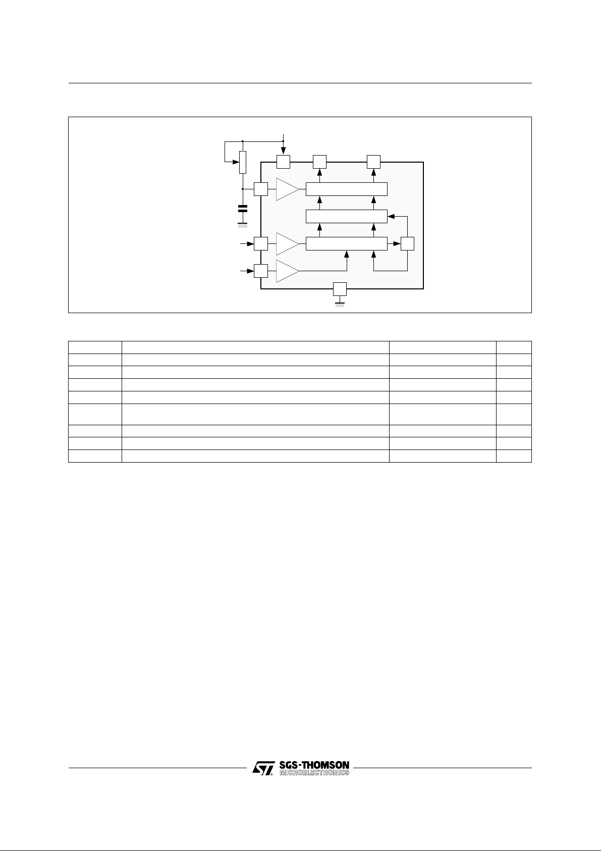
PIN CONNECTIONS
OUTPUT BIT 11
OUTPUT BIT 10
OUTPUT BIT 9
OUTPUT BIT 8
OUTPUT BIT 7
OUTPUT BIT 6
OUTPUT BIT 5
OUTPUT BIT 4
OUTPUT BIT 3
OUTPUT BIT 2
OUTPUT BIT 1
BRIGHTNESS CONTROL
1/2 digit
or to a
DD
V
SS
V
DD
DIP-28
(Plastic Package)
ORDER CODE : M5480B7
1
2
3
4
5
6
7
8
9
10
11
12
13
14
28
27
26
25
24
23
22
21
20
19
18
17
16
15
OUTPUT BIT 12
OUTPUT BIT 13
OUTPUT BIT 14
OUTPUT BIT 15
OUTPUT BIT 16
OUTPUT BIT 17
OUTPUT BIT 18
OUTPUT BIT 19
OUTPUT BIT 20
OUTPUT BIT 21
OUTPUT BIT 22
OUTPUT BIT 23
DATA IN
CLOCK IN
5480-01.EPS
May 1993
1/6
M5480
BLOCK DIAGRAM (Figure 1)
BRITGHTNESS
CONTROL
V
14
DD
OUTPUT
BIT 23
OUTPUT
BIT 1
1217
35 OUTPU T BUFERS
35 LATCHES
35 BIT SHIFT REGISTER
LOAD
RESET
1nF
SERIAL
DATA
CLOCK
13
16
15
1
ABSOLUTE MAXIMUM RATINGS
Symbol Parameter Value Unit
V
DD
V
V
O (off)
I
O
P
tot
T
T
oper
T
stg
Stresses in excess of those listed un der "Absolute Maximum Ratings" may cause permanent damage to the device. This is a s tress rating only
and functional operation of the device at these or any other conditions in excess of those in dicated in the operational sect ions of this specifi cation
is not implied. Exposure to absolute maximum rating conditions for extended periods may affect device reliability.
Supply Voltage – 0.3 to 15 V
Input Voltage – 0.3 to 15 V
I
Off State Output Voltage 15 V
Output Sink Current 40 mA
Total Package Power Dissipation at 25 °C
at 85 °C
Junction Temperature 150 °C
j
940
490
Operating Temperature Range – 25, + 85 °C
Storage Temperature Range – 65, + 150 °C
mW
mW
5480-02.EPS
5480-01 . TBL
2/6
 Loading...