

AND TONE GENERATION CIRCUIT
HW ANDSW COMPATIBLEWITH M116
1 TO 64 SERIAL CHANNELS PER FRAME
(CONTROLLEDBY SYNC SIGNAL PERIOD)
29 MAXIMUMCONFERENCES
1 TO 64 SERIAL CHANNELS PER CONFER-
ENCES
3 SIMULTANEOUS OPERATION MODES
AVAILABLE:
CONFERENCE, TRANSPARENT AND TONE
GENERATION
TYPICALBIT RATES:
1536/1544/2048/4096Kbits/s
COMPATIBLE WITH ALL KINDS OF PCM
FORMAT
µ ANDA LAW (PINPROGRAMMABLE)
EQUALPRIORITYTO EVERY CHANNEL
ONE FRAME AND ONE CHANNEL DELAY
FROMSENDINGTO RECEIVING
OVERFLOWINFORMATIONFOR EACHCON-
FERENCE BY PIN OS (OVERFLOW SIGNALLING) AND ON DATA BUS ON MPU REQUEST
INSTRUCTION SET COMPATIBLEWITH M3488
PROGRAMMABLE INPUT AND OUTPUT AT-
TENUATION OR GAIN FROM 0 TO 15dB
WITHSTEP OF 1dB FOR EACH CHANNEL
TONE GENERATION FROM 3.9Hz TO
3938HzWITH MIN. STEP OF 3.9Hz
TOTAL OF 7 DIFFERENT TONE OUTPUTS
IN PARALLEL PROGRAMMABLE VIA MPU
(MAXIMUM 4 DIFFERENT FREQUENCIES
ANDDURATIONS)
1 MELODY OF MAXIMUM 32 PROGRAMMABLE FREQUENCIES AND DURATIONS
5V POWER SUPPLY
TTL COMPATIBLE INPUT LEVELS,
CMOS/TTL COMPATIBLEOUTPUTLEVELS
MAIN INSTRUCTIONS CONTROLLED BY MI-
CROPROCESSORINTERFACE:
– Channelconnectionto a conference
– Channelattenuation or gain
– Channeldisconnectionfromboth conference
andtransparentmodes
– Tone and melody generation
– Overflowstatus
– Operatingmode
– Channelstatus
M34116
PCM CONFERENCECALL
PRELIMINARY DATA
DIP24
ORDERING NUMBER: M34116B1
PLCC28
ORDERING NUMBER: M34116C1
DESCRIPTION
The M34116 is a productspecificallydesignedfor
applications in PCM digital exchanges. It is able
to handle up to 64 channels in any conferences
combination from 1 to 29 conferences in parallel
and to generate seven different tones and one
melody.
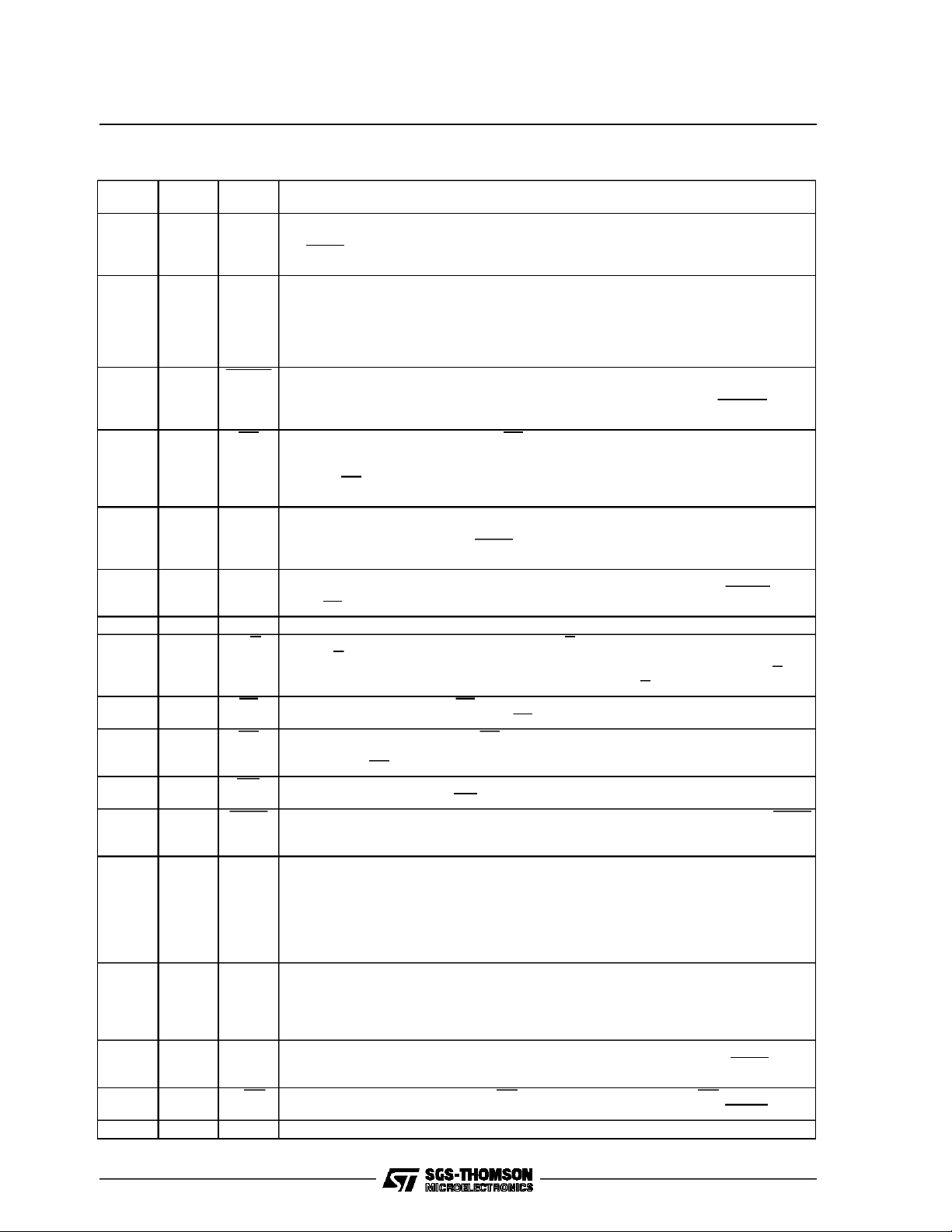
Theparties in a conferencemust previouslybeallocated through the Digital Switching Matrix
(M3488) in a single serial wire at M34116 PCM
input (IN PCMpin).
The M34116 is full pin and function compatible
with the M116. In addition, it has the capabilityto
generatetone directly coded in PCM.
For the conference function, each channelis converted inside the chip from PCM law to linear law
(14 bits). Then it is added to its conference, and
the sample of the previous frame is subtracted
fromthe conference.
In this way a new conferencesum signal is generated.
The channel output signal will contain the information of all the other channels in its conference
exceptits own.
After the PCM encoding, the data is serialized by
the M34116 in the same sequence as the PCM
input frame, with one frame (plus one channel)
delayand will be reallocated by the DSM (M3488)
at the final channel and bus position.
A programmable attenuation or gain can be set
on each channel and for every function: conference, tone generationand transparentmode.
January1995
This is advanced information on anew product now in development or undergoing evaluation. Details are subject to change without notice.
1/23
M34116
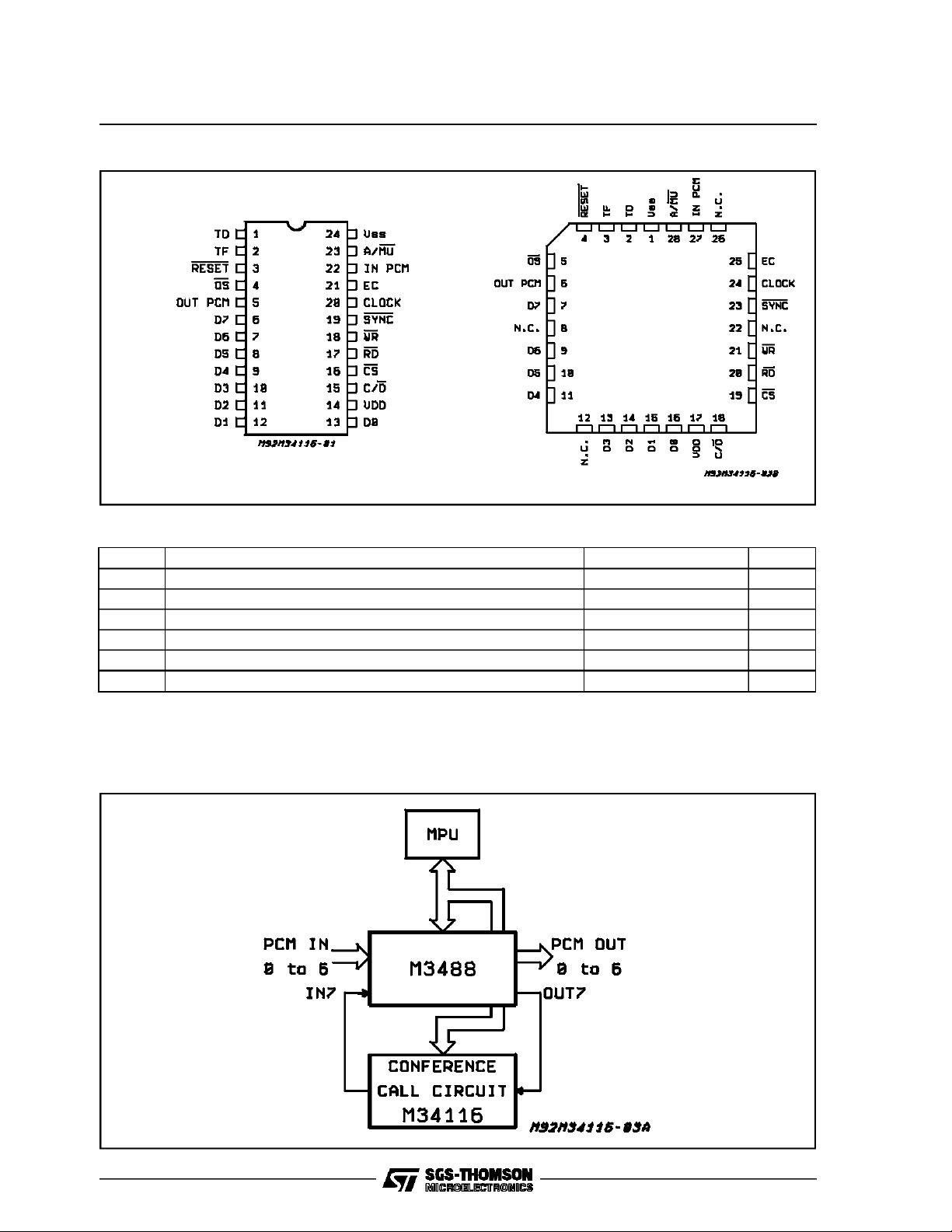
PIN CONNECTIONS (Topview)
DIP24
PLCC28
ABSOLUTE MAXIMUM RATINGS
Symbol Parameter Value Unit
(*) Supply Voltage – 0.3 to 7 V
V
DD
V
V
O (off)
P
T
T
Stresses above those listed under ”Absolute Maximum Ratings” may causes permanent damage to the device. This is a stress rating only and
functional operation of the device at these or any other conditions above those indicated in theoperational sectionsof this specification is not
implied. Exposure to absolute maximum rating conditions for extended periods may affect device reliability.
Input Voltage – 0.3 to V
i
DD
Off State Output Voltage – 0.3 to 7 V
Total Power Dissipation 500 mW
tot
Storage Temperature – 65 to 150 °C
stg
Operating Temperature 0 to 70 °C
op
Figure1: PCMConference Call InsertionScheme
2/23
PINDESCRIPTION
M34116
DIP
N
PLCC
o
o
N
Pin Function
1 2 TD M116 operating mode only. Tone Duration input pin. When TD = 1, a PCM coded tone
(instead of PCM data) is sent out to all channels enabled by the IT bit. TD is latched by
the SYNC signal so that all channels have the same tone during the same number of
frames. TD = 0 fornormal operation.
2 3 TF M116 operating mode only. Tone Frequency input pin. When TF = 1, the tone amplitude
is high. When TF = 0, the tone amplitude is low. TF is latched by SYNC. The PCM coded
tone level corresponds to 1/10 of the full scale. For M34116 operating mode: Melody
waveform select input pin. When TF = 1, the PCM output of the melody represents a
square wave. When TF = 0, it represents a sine wave. In both cases, the rms level is the
same and is equal to – 6 dBm0 if no attenuation or gain is programmed.
3 4 RESET Master reset input pin. This pin is active low and must be used at the very beginning after
power up to initialize the device or when switching from A law to Mu law. The Internal
initialization routine takes 2 time frames starting from the rising edge of RESET. During
thisinitialization time, all data bus and PCM output are pulled to a high impedance state.
4 5 OS Overflow Signalling output pin. When OS = 0 one conference is in overflow. This signal is
anticipated over halftimeslot with respect to the output channel involved in the conference in
overflow. Example: if output channel 4 is one of the parties of one conference in
overflow, OS = 0 during the second half of the time slot corresponding to output channel 3
andduring the firsthalf of thetime slot corresponding to output channel 4.
5 6 OUT
PCM
PCM output pin. The bit rate is 4096Kbits/s max. The sign bit is the first bit of the serial
sequence. The first bit of the first channel is found at the rising edge of the CLOCK signal
preceding the rising edge of the SYNC signal. The output buffer is open drain to allow for
multiple connections.
6to13 7,
9 to 11,
13 to 16
D0 toD7Bidirectional Data bus pins. Data and instructions are transferred to or from the
microprocessor. D0 is the Least Significant Bit. The bus is tristate when RESET is low
and/orCS is high.
14 17 VDD +5V Supply input. 100nF decoupling capacitor recommended.
15 18 C/D Control Data input pin. In a write operation C/D = 0 qualifies any bus content as data
while C/D = 1 qualifies it as an opcode. For M116 operating mode only: in a read
operation, the overflow information of the first eight conferences is selected by C/D = 0,
the overflow of the last two conferences andthe status by C/D = 1.
16 19 CS Chip Select input pin. When CS = 0, data and instructions can be transferred to or from
the external microprocessor and when CS = 1 the data bus is in tristate.
17 20 RD Read control input pin. When RD = 0, read operation is performed. When match
conditions for the opcode exists, data is transferred to the external microprocessor on the
fallingedge of RD.
18 21 WR Write control input pin. Instructions and opcode from the external microprocessor are
latchedon the rising edge of WR.
19 23 SYNC Synchronization input pin. The rising edge of CLOCK preceding the rising edge of SYNC
corresponds to the first bit of the first channel except for PCM frame of 1544Kbits/s. In
thiscase, it corresponds to the Extra bit (193th).
20 24 CLOCK Master Clock input pin. Typ.operating Frequencies are:
3.072MHz for 24 PCM channels frame (192 bit/frame)
3.088MHz for 24 PCM channels frame with extra bit (193 bit/frame)
4.096MHz for 32 PCM channels frame (256 bit/frame)
8.192MHz for 64 PCM channels frame (512 bit/frame)
Both M34116 an M116 operating modes are possible up to 4.096MHz.
At 8.192MHz only M34116 operating mode is possible.
21 25 EC External Clock output pin. This pin provides the master clock for the Digital Switching
Matrix (M3488). Normally it is the same signal as applied to the CLOCK input (pin 20).
When the Extra bit is selected with the instruction 5, the first two periods of the master
clock are canceled in order to allow the operation of the M34116 and the DSM with PCM
frame with Extra bit (e.g.193 bit/frame with PCM I/O of 1544Kbits/s).
22 27 IN PCM PCM input pin. The max bit rate is 4096Kbits/s. The first bit of the first cahnnel is found at
the second rising edge of the CLOCK signal following the rising edge of the SYNC signal.
If Extra bit is selected, then the firstbit is shifted by two CLOCK periods.
23 28 A/MU A Lawor MU Lawselectpin. WhenA/MU=1, A Lawisselected. WhenA/MU= 0, MULawis
selected. The law selection must be done before initializing thedevice using the RESET pin.
24 1 Vss Ground.
3/23
M34116
RECOMMENDED OPERATINGCONDITIONS
Symbol Parameter Value Unit
V
CC
V
i
V
O
CLOCK Freq. Input Clock Frequency 3.072/3.088
SYNC Freq. Input Synchronization Frequency 8 KHz
T
op
CAPACITANCES (measurementsfrequency= 1MHz; 0 to 70°C; unusedpins tied to VSS)
Symbol Parameter Pin (**) Min. Typ. Max. Unit
C
I
C
I/O
C
O
SupplyVoltage 4.75 to 5.25 V
Input Voltage 0 to 5.25 V
Off State Output Voltage 0 to 5.25 V
4.096 / 8.192 (*)
Operating Temperature 0 to 70 °C
Input Capacitance 1 to 3; 15 to 20; 22 to 23 5 pF
I/O Capacitance 6 to 13 15 pF
Output Capacitance 4, 5, 21 10 pF
MHz
MHz
ELECTRICALCHARACTERISTICS (Tamb = 0 to 70°C, VCC=5V±5%)
AllDC characteristicare valid 250µs after V
Symbol Parameter Pins (**) Test Condition Min. Typ. Max. Unit
V
IL
V
IH
V
T–
V
T+
V
HY
V
OL
V
OH
V
OL
I
IL
I
OL
I
CC
(*) Only in M34116 Operating Mode.
(**) Pin numbersreferred to the DIP24.
(***) Schimitt-trigger inputs.
Input Low Level 1 to 3
15 to 20
22 to 23
Input High Level 1 to 3
15 to 20
22 to 23
Negative Threshold
6 to 13 (***) VCC= 5V 0.6 0.9 1.1 V
Voltage
Positive Threshold
6 to 13 (***) VCC = 5V 1.5 1.7 2 V
Voltage
Hysteresis 6 to 13 (***) VCC= 5V 0.4 0.8 V
Output Low Level 4,6 to 13,21 IOL= 2mA 0.4 V
Output High Level 4 to 13, 21 IOH = 1mA VCC-0.4 V
Output Low Level 5 IOL = 4.1mA 0.4 V
Input Leakage Current 1 to 3
6to13
15 to 20
22 to 23
Data Bus Leakage
6to13 VIN= 0 to V
Current
Supply Current 14 Clock Freq. = 4.096MHz 50 mA
andclock have been applied.
CC
V
= 0 to V
IN
CS = V
CC
CC
CC
– 0.3 +0.8 V
2.0 V
CC
10 µA
±10 µA
V
4/23

M34116
ELECTRICALCHARACTERISTICS (Tamb = 0 to 70°C, VCC=5V±5%)
All DC characteristic are valid 250µs after V
load and R
Signal Symbol Parameter Test Condition Min. Typ. Max. Unit
CK
Up to
4.096MHz
CK
8.192MHz
SYNC t
PCM
Input
PCM
Output
(Open
drain)
RESET t
WR t
RD t
Notes:
1. With Extra Bit operatingmode insert this time becomes 3 t
2. With Extra Bit operatingmode insert these times are 80ns longer.
3. With OPCODE (C/D = I), this time becomes 4tck (6tck if E = 1). E: extra bit indication in”operating mode” instruction.
4. For tone generation instruction, this time becomes 4tck (6tck if E =1) E: extra bit indication in ”operating mode” instruction.
5. With extra bit operating mode insert, this time becomes 6tck.
6. The initialization routine takes2 frames time starting from the rising edge of RESET - Anyaccess to the device should take place after the
initialization routine is completed. (2 frames time).
the test pull up resistor.
L
t
CK
t
WL
t
WH
t
R
t
F
t
CK
t
WL
t
WH
t
R
t
F
SL
t
HL
t
SH
t
WH
t
S
t
H
t
PD min.
Clock Period
Clock Low Level Width
Clock High Level Width
Rise Time
Fall Time
Clock Period
Clock Low Level Width
Clock High Level Width
Rise Time
Fall Time
Low Level Set-up Time
Low Level Hold Time
High Level Set-up Time
High Level Width
Set-up Time
Hold Time
Propagation Time Low
Level referred to CK
t
PD max.
Propagation Time High
level Referred to CK
t
t
t
t
t
REP
SL
HL
SH
WH
WL
WH
Low Level Set-up Time
Low Level Hold Time
High Level Set-up Time
High Level Width
Low Level Width
High Level Width
Repetition interval
between active pulses.
t
SH
High Level st-up time to
active read strobe.
t
HH
High Level hold time to
active read strobe.
Rise Time
Fall Time
Low Level Width
High Level Width
Repetition interval
t
t
REP
t
t
WL
WH
R
F
between active pulses.
t
SH
High Level st-up time to
active read strobe.
t
HH
High Level hold time to
active read strobe.
t
R
t
F
Rise Time
Fall Time
and clock have been applied. CLis the max. capacitive
CC
230
100
100
25
25
120
50
50
10
10
See note 1 30
30
30
t
CK
35
35
CL = 50pF RL=1KΩ 40
180
note 6 50
30
30
t
CK
150
200
note 3 and 4
500
0
20
60
60
180
200
note 5
4t
CK
0
20
60
60
.
CK
ns
ns
ns
ns
ns
ns
ns
ns
ns
ns
ns
ns
ns
ns
ns
ns
ns
ns
ns
ns
ns
ns
ns
ns
ns
ns
ns
ns
ns
ns
ns
ns
ns
ns
ns
ns
5/23
M34116
ELECTRICALCHARACTERISTICS (continued)
Signal Symbol Parameter Test Condition Min. Typ. Max. Unit
CS
CD
OS t
EC t
TD/TF t
D0 to D7
(interface
bus)
t
SL (CS-WR)
t
HL (CS-WR)
t
SH (CS-WR)
t
HH (CS-WR)
t
SL (CS-RD)
t
HL (CS-RD)
t
SH (CS-RD)
t
HH (CS-RD)
t
S(C/D-WR)
t
H(C/D-WR)
t
S(C/D-RD)
t
H(C/D-RD)
PD(OS)
PD(EC)
S
t
H
t
S(BUS-WR)
t
H(BUS-WR)
Low level set-up time
to WR falling edge.
Low Level hold time from
WR rising edge.
High level set-up time to
WR falling edge.
High level hold time from
WR rising edge.
Low level set-up time
to RD falling edge.
Low Level hold time from
RD rising edge.
High level set-up time to
RD falling edge.
High level hold time from
RD rising edge.
Set-up time to write strobe
end.
Hold time from write
strobe end.
Set-up time to read strobe
start.
Hold time from read
strobe end.
Propagation time from
risingedge of CK.
Propagation time referred
to CK edges.
Set-up
Hold Time
Input set-up time to write
strobe end.
Input hold time from write
strobe end.
Active Case
Active Case
Inactive Case
Inactive Case
Active Case
Active Case
Inactive Case
Inactive Case
CL= 50pF 100 ns
CL= 50pF 30 ns
0
20
0
20
0
0
0
0
130
25
20
25
80
40
130
25
ns
ns
ns
ns
ns
ns
ns
ns
ns
ns
ns
ns
ns
ns
ns
ns
t
PD(BUS)
Propagation time from
(active) falling edge of
read strobe.
t
HZ(BUS)
Propagation time from
(active) rising edge of
read strobe to high
impedance state.
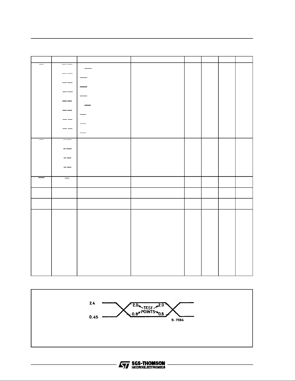
A.C. TESTING, OUTPUT WAVEFORM
A.C. testing inputs are driven at 2.4V for a logic ”1” and 0.45V for a logic ”0”,timing
measurementare made at 2.0V for a logic ”1” and 0.8V for a logic ”0”.
6/23
CL = 200pF
120
80
ns
ns
Figure2: InsertionSchema of M34116in a 480 x 480 Non-BlockingDigital Switching Matrix
M34116
Figure3: Block Diagram
EC RESET
CLOCK
SYNC
IN PCM
TIMING
SR
FRAME
RAM
POWER
10
14
8
OS A/MU CS WR C/D RD
MPU INTERFACE
PCM
to
LOG LIN
14
ADDER
19
TONE
ROM
LIN
to
PCM
TONE
CONTROL
19
CONF
RAM
SR
DB(7:0)
TF
TD
OUT PCM
D94TL130
7/23

M34116
CIRCUITDESCRIPTION
ALGORITHMS
♦ Conference. For each channel,the PCM signal
coming in is added to its conference and the
PCM signal of the previous frame is subtracted
to its conference before being sent out. The
output signal contains only the data of all the
other channels in its conference except its
own.
♦ Tone. A fourth of a sine wave equivalent to
3.9Hz(8KHz/2048) is stored in a ROMwhich is
read at multiple of the step (modulus 512)
equivalentto the specified frequency. This step
is used until the duration is reached then a
new step will be used according to the specified sequence.
♦ Attenuation gain. The PCM signal is converted
to logarithmic of the equivalent linear and then
added or subtracted to the specified level. It is
then raised to the power of 10 to be converted
backto linear.
ARCHITECTURE
The basic time slot (16 periods of the master
clock) is divided in four different parts that perform four different operations (also refer to Fig. 2
block diagram):
# input processing: attenuation or gain of input
PCM according to the algorithm mentioned
earlier. The serial PCM signal coming in is
loadedas 8 bits parallel and convertedto logarithmic of the linear (through the PCM to LOG
LIN block). It is then added to the attenuation
or gain levels (also in logarithmic) stored in the
MPU interface, the result is raised to the power
of 10 (through the POWER 10 block) to be
converted back to linear and written in the
FRAMERAM.
# conference addition: the above PCM signal,
amplifiedor attenuatedand converted in linear,
is added to the conference and the result is
stored in the conference RAM (block CONF
RAM).
# conferencesubtraction: the signal stored in the
FRAMERAM during the previous frame is subtracted to the conference and the result is
stored in the conferenceRAM.
# output processing: attenuation or gain of the
PCM to be sent out. The result of the above
substraction is converted to PCM (through the
block LIN to PCM) and to logarithmic (through
the block PCM to LOG LIN), added to the attenuation or gain level stored in the MPU interface, converted to linear (through the block
POWER 10) and then to PCM (through the
block LIN to PCM). The resulting 8 bits are
then shiftedout serially.
If a channel is in conference, then all the four
above operations are applied. If it is in transparent mode, then only the first and last operations
are applied. For tone generation, the two first operations are not used. During the third part, the
tone ROM is read. Since the ROM data is in linear it can therefore be applied to the fourth operationfor output processing.
By default, after reset, the M34116 has the functionality and the instruction set of the M116. With
a new operating mode instruction, the user can
selectthe functionality of the M34116 with its new
instructionset. The instructionset includes:
◊ operating mode: the user can choose either the
M116 mode or the M34116 mode, the PCM
byte format (no bit inverted, even bit inverted,
odd bit inverted or all bit inverted) and the
presenceor not of the extra bit.
◊ conferenceconnection:the user specifies which
channel to be connected to which conference
withthe attenuationor gain levels to be applied
to the PCM signal comingin and/orsent out.
◊ transparentconnection:theuser specifies which
channel to be connected in transparent mode
(bypass mode) with the attenuationor gainlevels to be applied to the PCM signal coming in
and/orsent out.
◊ tone generation: the user specifies to which
channel the tone must be sent out with the attenuation or gain levels and the tone sequence. The sequence is composed of maximum4 pairs of frequency-durationfor tone and
maximum 32 pairs of frequency-duration for
melody. The frequency range is 3.9Hz to
3938Hz and the duration range is from 32ms
to 8610ms. The user can specify either all of
the pairs or finish the sequence with the byte
hex FF. The M34116 will loop the specified sequence endlessly or until the channel is disconnected. The melody could be either a sine
or square wave (pin programmable).
◊ channeldisconnection:the userspecifies which
channel to be disconnected. A disconnected
channel can be reconnected only after a minimumof one frame time.
◊ overflow status. The userspecifies which of the
4 banks of 8 conferences to be monitored and
the M34116 will send the status byte at the
readoperation.
◊ channel status. The user specifies the channel
number and the M34116 will send out the
status bytes at the read operation. These bytes
include: conference number or transparent
mode or tone or no connection, input attenuation or gain levels, output attenuation or gain
levels. If the channel is in the tone mode, the
tone sequence of frequency and duration will
also be sent out.
8/23

M34116
INSTRUCTION SET
OPERATINGMODES
Two different operating mode istructions are available:
M116 Operating Mode:
Sending this operating mode instruction, the device functionalityis the same as M116 and M116 instruction set is selected(refer to the following M116 instruction set for furtherdetails).
Control Signal Data Bus
CS RD C/D WR D7 D6 D5 D4 D3 D2 D1 D0
0110XEF1F00101
❖ E = 1 extra bit
❖ F1– F0 = 00 no bit inverted
01 even bit inverted
10 odd bit inverted
Default valuesafter reset:
E = 0 F1– F0 = 11 if MU Law
F1– F0 = 01 if A Law
11 all bit inverted
M34116 Operating Mode:
Sending this operating mode instruction, the M34116instruction set and functionalityare selected
Control Signal Data Bus
CS RD C/D WR D7 D6 D5 D4 D3 D2 D1 D0
0110XEF1F01001
❖E = 1 extrabit
❖F1–F0 = 00 no bit inverted
01 even bit inverted
10 odd bit inverted
11 all bit inverted
Note:
Upon reset M116 instruction set is automatically
selected. To switch from the M116 instruction set
the above M34116 operating mode instruction is
necessary. The operating mode instruction, when
necessary, mustbe sentjust afterreset.
M34116 INSTRUCTION SET.
INSTRUCTION 1: M34116 CHANNEL CONNECTION IN CONFERENCEMODE
Five bytes are needed:
Control Signal Data Bus
CS RD C/D WR D7 D6 D5 D4 D3 D2 D1 D0
0 1 0 0 X X S P4P3P2P1P0
0 1 0 0 X X X Al4 Al3 Al2 Al1 Al0
0 1 0 0 X X X AO4 AO3 AO2 AO1 AO0
0 1 0 0 X PTC5C4C3C2C1C0
0110XXXX0111
❖ S: Startbit
❖ Al4–Al0:
Al4 =1
Al4 =0
Al3–Al0
❖ Ol4–AO0:
AO4 = 1
AO4 = 0
AO3–AO0
Input attenuationor gain(±15dB)
gain
attenuation
value indB (0–15)
outputattenuationor gain(±15dB)
gain
attenuation
value indB (0–15)
❖ PT: Phase toggle conference
❖ P4–P0:Conferencenumber(1–29)
❖ C5–C0:Channel number (0–63)
WhenS = 1 theconferenceregister is cleared.
S = 1 can be used only when connecting the first
channelto a new conference.
When PT = 1 the sign of the PCM samples is
changed before they are put in conference. This
correspondsto a phase shift of 180° and may be
usedto reduce the electrical echo.
Note:Unspecified DataBuscanbeeither0’s or 1’s
9/23

M34116
M34116 INSTRUCTION SET (continued)
INSTRUCTION 2: M34116 CHANNEL CONNECTION IN TRANSPARENTMODE
Four bytes are needed:
Control Signal Data Bus
CS RD C/D WR D7 D6 D5 D4 D3 D2 D1 D0
0 1 0 0 X X X Al4 Al3 Al2 Al1 Al0
0 1 0 0 X X X AO4 AO3 AO2 AO1 AO0
0 1 0 0 X X C5 C4 C3 C2 C1 C0
0110XXXX0011
❖Al4–Al0:
Al4 =1
Al4 =0
Al3–Al0
Input attenuationor gain(±15dB)
gain
attenuation
value indB (0–15)
❖ AO4–AO0:
AO4 = 1
AO4 = 0
AO3–AO0
outputattenuationor gain (±15dB)
gain
attenuation
value indB (0–15)
❖ C5–C0:Channel number (0–63)
INSTRUCTION 3: M34116CHANNEL DISCONNECTION
This instruction is necessary to disconnect a party from a conference, to end a transparent mode connectionor to end a tone generation.
Two bytes are needed (same formatas M116):
Control Signal Data Bus
CS RD C/D WR D7 D6 D5 D4 D3 D2 D1 D0
0 1 0 0 X X C5 C4 C3 C2 C1 C0
0110XXXX1111
# C5–C0:Channel number (0–63)
One time frame must exist between disconnectionand connectionof the same channel.
INSTRUCTION 4: M34116 OVERFLOWINFORMATION
Single byte instruction:
Control Signal Data Bus
CS RD C/D WR D7 D6 D5 D4 D3 D2 D1 D0
0110XXB1B01010
❖B1–B0: Bank Selection (0–3)
Conference overflow information is sent out, after this instruction, in the data bus (D7–D0) when RD
goes low according to the Bank selection value:
Control Signal
CS RD C/D WR B1 B0 D7 D6 D5 D4 D3 D2 D1 D0
0001007654321X
0 0 0 1 0 1 15 14 13 12 11 10 9 8
0 0 0 1 1 0 23 22 21 20 19 18 17 16
0 0 0 1 1 1 X X 29 28 27 26 25 24
10/23
Bank
Selection
Conference Number

M34116
M34116 INSTRUCTION SET (continued)
INSTRUCTION 5: M34116 TONE GENERATION
Up to 7 Tone and 1 Melody channels may be activesimultaneously. The instructionformat for Tone and
Melody is the same. For each Tonechannel from 1 up to 4 couples of Step/Timemay be specified while
for the Melody channelfrom 1 up to 32 couplesof Step/Timemaybe specified.
Note:
The Melody channelcan be channel0 or 8 or 16 or24 etc. accordingto the following formula:
Melodychannel number = 0 + 8
The Tone channel assignment followsthesame rule:
Tone 1 channelnumber = 1 + 8
Tone 2 channelnumber = 2 + 8
... ..................... ... ..................
Tone 7 channelnumber = 7 + 8
This means that, selecting the tone 1 on the channel 9 (or and other one of its series), the channels 1,
17, 25.... cannot be used for tones (or melody). The same is occuringfor the tones 2...7 or the melody.
Control Signal Data Bus
CS RD C/D WR D7 D6 D5 D4 D3 D2 D1 D0
0 1 0 0 AO4 AO3 AO2 AO1 AO0
0 1 0 0 C4 C3 C2 C1 C0
0110 1100
0 1 0 0 S17 S16 S15 S14 S13 S12 S11 S10
0 1 0 0 T17 T16 T15 T14 T13 T12 T11 T10
0 1 0 0 S27 S26 S25 S24 S23 S22 S21 S20
0 1 0 0 T27 T26 T25 T24 T23 T22 T21 T20
::::::::::::
optionalend code:
x n (n = 0, 1, 2, 3, 4, 5, 6, 7)
x n (n = 0, 1, 2, 3, 4, 5, 6, 7)
x n (n = 0, 1, 2, 3, 4, 5, 6, 7)
x n (n = 0, 1, 2, 3, 4, 5, 6, 7)
010011111111
opcode:
0110 1100
❖AO4–AO0:Outputattenuationor gain (±15dB) AO4 = 1 gain, AO4 = 0 attenuation,
AO3–AO0valuein dB (0–15)
0dB attenuationor gain correspondto -6dBm0 level.
❖ C5–C0:Channelnumber (0–63)
❖ Sn7–Sn0:FrequencyStep for the n–th note in the tone sequence (n = 1–4 for tone n = 1–32 for
melody).Stepis a compressedcoding of the frequencyvalue. Givena frequencyvaluef the value of
S7–S0can be calculatedas follow:
1) calculate the linear step SL = round ( f
2) apply the followingtable to get S7–S0value from SL value (see also Appendix1A and 1B).
S7 S6 Linear Step SL value (10 bit) (SL decimal) STEP (Hz)
0 0 0 0 0 0 S5 S4 S3 S2 S1 S0 (1→64) (*) 3.9
0 0 0 0 0 1 S5 S4 S3 S2 S1 S0 (65–>127) (**) 3.9
0 1 0 0 1 S5 S4 S3 S2 S1 S0 0 (128–>254) 7.8
1 0 0 1 S5 S4 S3 S2 S1 S0 0 0 (256–>508) 15.6
1 1 1 S5 S4 S3 S2 S1 S0 0 0 0 (512–>1008) 31.2
x
32
125
)
(*) For tone 7 only; (**) For melodyand tone 1-6
Note: to obtaina Pause (Silence) –> S7–S0 must be all 0’s
❖ Endcode: if Less than 4 couplesof Step/Timefor toneor less than 32 for melody are to be specified
thenafter the last coupleof Step/Time a Step of all1’s (optional end code) must be sentbefore the
opcode. Otherwiseit must be skipped.
❖ Tn7–Tn0:Specify the duration of the n’th note or pause. The time increment is 32ms. To get T7–T0
value, divide the wanted duration in ms by 32 and round to integer.
Note: The minimum time between rising edges of successiveWR for tone generationinstruction is 4ck
periods(6ck periods if EC = 1).
11/23

M34116
M34116 INSTRUCTION SET (continued)
INSTRUCTION 6: M34116 STATUS
The Status instruction can be used to read the contents of the instruction register and of the tone and
melodyregisters.
Two byte are needed:
Control Signal Data Bus
CS RD C/D WR D7 D6 D5 D4 D3 D2 D1 D0
0 1 0 0 C5 C4 C3 C2 C1 C0
0110 0110
❖C5–C0:Channel number (0–63)
After sending this instruction a variablenumber of Read can be sent depending on the type of operation
that performs the channel (conference, transparent, tone, or melody). The first 3 Read, common to all
type of operation,willsend on the Data Bus the followingdata relative to the channel (C5–C0):
Control Signal Data Bus
CS RD C/D WR D7 D6 D5 D4 D3 D2 D1 D0
0 0 0 1 IT PT P4 P3 P2 P1 P0
0 0 0 1 AI4 AI3 AI2 AI1 AI0
0 0 0 1 AO4 AO3 AO2 AO1 AO0
Note:
P4–P0= 0 means that the channelis disconnectedso any followingdataread is meaningless.
P4–P0= 1 to 29is the conferencenumber.
P4–P0= 30 means that the channel operation is Tone or Melody.
P4–P0= 31 means that the channel operation is transparentconnection.
If the channel operation is Tone or Melody (P4 – P0 = 30) then the subsequent Read will send on the
DataBus the couplesof Step/Time:
Control Signal Data Bus
CS RD C/D WR D7 D6 D5 D4 D3 D2 D1 D0
0 0 0 1 S17 S16 S15 S14 S13 S12 S11 S10
0 0 0 1 T17 T16 T15 T14 T13 T12 T11 T10
0 0 0 1 S27 S26 S25 S24 S23 S22 S21 S20
0 0 0 1 T27 T26 T25 T24 T23 T22 T21 T20
::::::::::::
Notes:
–Toneand Melodystatus readingends if anall 1’s Step value is found, otherwisethe readingiscyclic.
–The minimum time from the rising edge of the WR (with opcode) to the falling edge of first RD is 4clock
periods(6clockperiodsif E = 1) unlesstheselectedchannelhasbeendisconnected.In thiscase,one
time frame must existbetween the disconnect command and theread status command. The RD period
isminimum4clock periods(6clockperiods if E = 1).
– for both modes (M34116 and M116) the minimum time between two successive rising edges of the
WR with opcode (C/D = 1) is 4clock periods (6clock periods if E =1).
E: Extrabit indication in ”Operatingmode”instruction.
12/23

M34116
M116 INSTRUCTION SET
INSTRUCTION 1: CHANNELCONNECTION IN CONFERENCEMODE
Threebyte areneeded:
1)Thefirst byte containsthe conferencenumber (bits D0–D3) and the Start bit S (bit D4). When S = 1, all
registers of the conference will be cleared. S = 1 is only required in the instruction 1 set of the first
channel connectedto a new conference.
2)The second byte contains in the bits (D0–D4) the number of the channel to be connected and the In-
sert Tone Enable bit IT (D5). When bit IT = 1 all the channels belonging to that conference are enabled using insert tone function if it’sactive (TD = 1).
3) The third byte containsinformationabout the attenuationlevel to be applied to that channel and the
opcode (0111).
Instruction1 Format
Control Signal Data Bus
CS RD C/D WR D7 D6 D5 D4 D3 D2 D1 D0
0 1 0 0 X X X S P3 P2 P1 P0
0 1 0 0 X X IT C4 C3 C2 C1 C0
0110A1A0XX0111
S: ConferenceStartbit
P3–P0:Conferencenumber (1–10)
IT: InsertionTone function enable (IT = 1)
C4–C0:Channel number(0–31)
A1–A0:Channel attenuation
00 = – 0dB
01 = – 3dB
10 = – 6dB
INSTRUCTION 2: CHANNELCONNECTION IN TRANSPARENTMODE
Two bytes are needed:
1) The first byte containsthe number of the channel.
2) The second byte contains informationabout the attenuationlevel to be applied to that channel and the
opcode (0011).
PCM data of this channel is notadded to any conference and it is transferredto the PCM output. It is not
affectedby the tone control pins.
Instruction2 Format
Control Signal Data Bus
CS RD C/D WR D7 D6 D5 D4 D3 D2 D1 D0
0 1 0 0 X X X C4C3C2C1C0
0110A1A0XX0011
INSTRUCTION 3: CHANNELDISCONNECTION
Two bytes are needed:
1) The first word contains the number of the channelto be disconnected.
2) The second word containstheopcode (1111).
One time frame must exist between disconnectionand connectionof the samechannel.
Instruction3 Format
Control Signal Data Bus
CS RD C/D WR D7 D6 D5 D4 D3 D2 D1 D0
0 1 0 0 X X X C4C3C2C1C0
0110XXXX1111
13/23

M34116
M116 INSTRUCTION SET (continued)
INSTRUCTION 4: OVERFLOWINFORMATION
Two bytes are needed to know the status of all 10 conferences:C/D = 0 reads the first byte (first 8 con-
ferences) and C/D = 1 reads the second byte (the last 2 conferences).A conference is in overflow when
the corresponding bit is high.
Instruction4 Format
Control Signal Data Bus
CS RD C/D WR D7 D6 D5 D4 D3 D2 D1 D0
0 0 0 1 CF8 CF7 CF6 CF5 CF4 CF3 CF2 CF1
0011XXXXXXCF10 CF9
CF10 – CF1: Conference in overflow when high.
nb: as long as RD remains low, the overflow status of the conference selected by C/D can be monitored
in real time.
INSTRUCTION 5: OPERATINGMODE
The single byte needed contains the Extra bit (D6), the format bits F1–F0 (D5–D4) and the opcode
(0101).
The E bit must be E = 1 when the PCM frame contains a number of bit multiple of eight plus on bit (ex.
PCM frame at 1544Kbit/s).Normally E = 0. The bits F1–F0 select the kinds of PCM format byte according table 1. After Reset the default values corresponds to F1 = 0, F0 = 1 if A–law is selectedand F1 = 1,
F0 = 1 if Mu–law is selected. All channels must be disconnectedwhen the OperatingMode Instructionis
sent. They must remaindisconnectedfor at least two time framesafter the instructionwas sent.
We recommende to usethis instruction right after the RESET (see pin RESET decription).
Instruction5 Format
Control Signal Data Bus
CS RD C/D WR D7 D6 D5 D4 D3 D2 D1 D0
0110XEF1F00101
E: Extrabit insertion (active when E = 1)
F1 – F0: PCM byte Formatselection(see also table 1)
00 = no bit inverted
01 = even bit (B0–B2–B4–B6)inverted
10 = odd bit (B1–B3–B5)inverted
11 = all bit (B0–B1–B2–B3–B4–B5–B6)inverted
INSTRUCTION 6: STATUS
Threebytes areneeded:
1) The first byte containsthe number of the channel;
2) The second byte contains the opcode (0110);
3) By a reding cycle you extract from the third byte the information about the operating mode of the
channel (no connection or transparentmode or number of the conference, bits D4–D7); the attenuation
(D2–D3)and noise suppression values(D0–D1) eventuallyinserted.
This reading cycle must be executedat least one frame after the end of the opcode writing cycle.
Instruction6 Format
Control Signal Data Bus
CS RD C/D WR D7 D6 D5 D4 D3 D2 D1 D0
0 1 0 0 X X X C4C3C2C1C0
0110XXXX0110
0 0 1 1 P3 P2 P1 P0 A1 A0 T1 T0
P3–P0: channelmode operation information
0000 = no connection
1111 = transparent mode
P3–P0give the number of the conferenc
nb: the instruction 6 enables the dat bus to read
the status until reset by C/D = 0 and WR = 1.
1010 – 0001 = conference mode
14/23

M34116
Table 1 : PCM Byte Format. B7(sign–bit) is the MSB and B0 is the LSB. F1–F0corresponds toD5–D4
in the byte of the Operating Mode Instruction(instruction5).
F1 F0 B7 B6 B5 B4 B3 B2 B1 B0
00
00
10
+FULL SCALE
MIN LEVELS
–FULL SCALE
+FULL SCALE
MIN LEVELS
–FULL SCALE
+FULL SCALE
MIN LEVELS
–FULL SCALE
1
1
0
0
1
1
0
0
1
1
0
0
1
0
0
1
0
1
1
0
1
0
0
1
Figure11: OverflowControlwith µP InteractiveProcedure
1
0
0
1
1
0
0
1
0
1
1
0
1
0
0
1
0
1
1
0
1
0
0
1
1
0
0
1
1
0
0
1
0
1
1
0
1
0
0
1
0
1
1
0
0
1
1
0
1
0
0
1
1
0
0
1
0
1
1
0
1
0
0
1
0
1
1
0
0
1
1
0
15/23

M34116
Figure12: SYNC,PCM I/O, RESET,TD/TFTimings
(1) t
correspondsto bit 0,channel 0or Extra Bit.
bit
Figure13: WRITEOperatingTiming.
16/23

Figure14: READ OperatingTiming.
M34116
Figure15: RC (External Clock) and OS (Overflow Signalling) Timings.
Figure16: EC Timing with ExtraBit OperatingMode Insert.
Figure17: OS Timing with Output PCMChannel n+1 belonging to a Conferencein Overflow.
17/23

M34116
APPENDIX1A - Correspondancebetween S7-S0 values(HEX)andsynthetizedfrequencyformelodyand
tone1-6:
18/23

M34116
APPENDIX1B - CorrespondencebetweenS7-S0values (HEX) and synthetizedfrequencyfor tone 7:
19/23

M34116
APPENDIX2
TONE GENERATIONPROGRAMMING
Example 1:
f = 425Hz
Duration 200ms ON, 200ms OFF, 600ms ON, 1000ms OFF
Attenuation10dB
Channel#0.
Programmingsequence:
Control Signal Data
CS RD C/D WR D7 . . . . D0
0100 0AH
0100 00H
0110 0CH
0100 2DH
0100 06H
0100 00H
0100 06H
0100 2DH
0100 12H
0100 00H
0100 1FH
0110 0CH
Example 2:
f = 400Hz
Duration:375ms ON, 375ms OFF
Attenuation5dB
Channel#3
Programmingsequence:
Control Signal Data
CS RD C/D WR D7 . . . . D0
0100 05H
0100 03H
0110 0CH
0100 26H
0100 0CH
0100 00H
0100 0CH
0100 FFH
0110 0CH
20/23

PLCC28PACKAGE MECHANICAL DATA
M34116
DIM.
MIN. TYP. MAX. MIN. TYP. MAX.
A 12.32 12.57 0.485 0.495
B 11.43 11.58 0.450 0.456
D 4.2 4.57 0.165 0.180
D1 2.29 3.04 0.090 0.120
D2 0.51 0.020
E 9.91 10.92 0.390 0.430
e 1.27 0.050
e3 7.62 0.300
F 0.46 0.018
F1 0.71 0.028
G 0.101 0.004
M 1.24 0.049
M1 1.143 0.045
mm inch
21/23

M34116
DIP24 PACKAGEMECHANICAL DATA
DIM.
MIN. TYP. MAX. MIN. TYP. MAX.
a1 0.63 0.025
b 0.45 0.018
b1 0.23 0.31 0.009 0.012
b2 1.27 0.050
D 32.2 1.268
E 15.2 16.68 0.598 0.657
e 2.54 0.100
e3 27.94 1.100
F 14.1 0.555
I 4.445 0.175
L 3.3 0.130
mm inch
22/23

M34116
Information furnished is believed to be accurate and reliable. However, SGS-THOMSON Microelectronics assumes no responsibility for the
consequences of use of such information nor for any infringement ofpatents or other rights of third parties which may resultfrom its use. No
license is granted by implication or otherwise under any patent or patent rights of SGS-THOMSON Microelectronics. Specifications mentioned in this publication are subject to change without notice. This publication supersedes and replaces all information previously supplied.
SGS-THOMSON Microelectronics products are not authorized for use as critical components in life support devices or systems without express written approval of SGS-THOMSON Microelectronics.
1995 SGS-THOMSON Microelectronics - All RightsReserved
SGS-THOMSON Microelectronics GROUPOF COMPANIES
Australia - Brazil - France - Germany - Hong Kong - Italy - Japan - Korea - Malaysia - Malta - Morocco - The Netherlands- Singapore -
Spain - Sweden - Switzerland - Taiwan - Thaliand - United Kingdom - U.S.A.
23/23
 Loading...