

Datasheet M29W800AT90N6T, M29W800AT90N6, M29W800AT90N1T, M29W800AB90N1T, M29W800AB90N1 Datasheet (SGS Thomson Microelectronics)
...
1/33March 2000
M29W800AT
M29W800AB
8 Mbit (1Mb x8 or 512Kb x16, Boot Block)
Low Voltage Single Supply Flash Memory
■ 2.7V to 3.6V SUPPLY VOLTAGEfor
PROGRAM, ERASE and READ OPERATIONS
■ ACCESS TIME: 80ns
■ PROGRAMMING TIME: 10µs typical
■ PROGRAM/ERASE CONTROLLER(P/E.C.)
– Program Byte-by-Byte or Word-by-Word
– Status Register bits and Ready/Busy Output
■ SECURITY PROTECTION MEMORY AREA
■ INSTRUCTION ADDRESS CODING: 3 digits
■ MEMORY BLOCKS
– Boot Block (Top or Bottomlocation)
– Parameter andMain blocks
■ BLOCK, MULTI-BLOCK and CHIP ERASE
■ MULTI BLOCK PROTECTION/TEMPORARY
UNPROTECTION MODES
■ ERASE SUSPEND and RESUME MODES
– Read and Program another Block during
Erase Suspend
■ LOW POWER CONSUMPTION
– Stand-by and Automatic Stand-by
■ 100,000 PROGRAM/ERASE CYCLES per
BLOCK
■ 20 YEARS DATA RETENTION
– Defectivity below 1ppm/year
■ ELECTRONIC SIGNATURE
– Manufacturer Code:20h
– Top Device Code, M29W800AT: D7h
– Bottom Device Code, M29W800AB: 5Bh
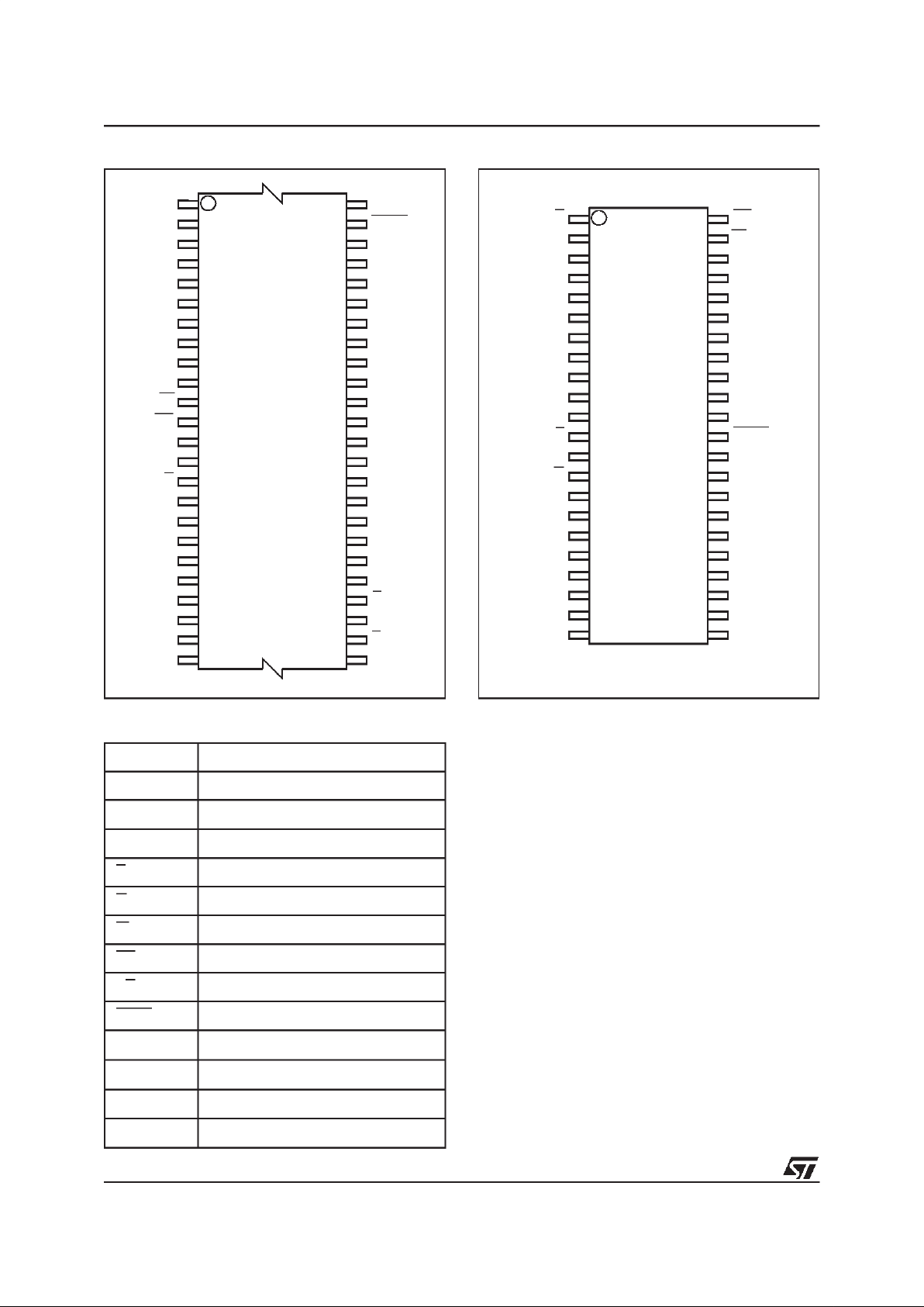
Figure 1. Logic Diagram
AI02599
19
A0-A18
W
DQ0-DQ14
V
CC
M29W800AT
M29W800AB
E
V
SS
15
G
RP
DQ15A–1
BYTE
RB
44
1
FBGA
TSOP48(N)
12 x 20mm
SO44 (M)
LFBGA48 (ZA)
8 x 6 solder balls
M29W800AT, M29W800AB
2/33
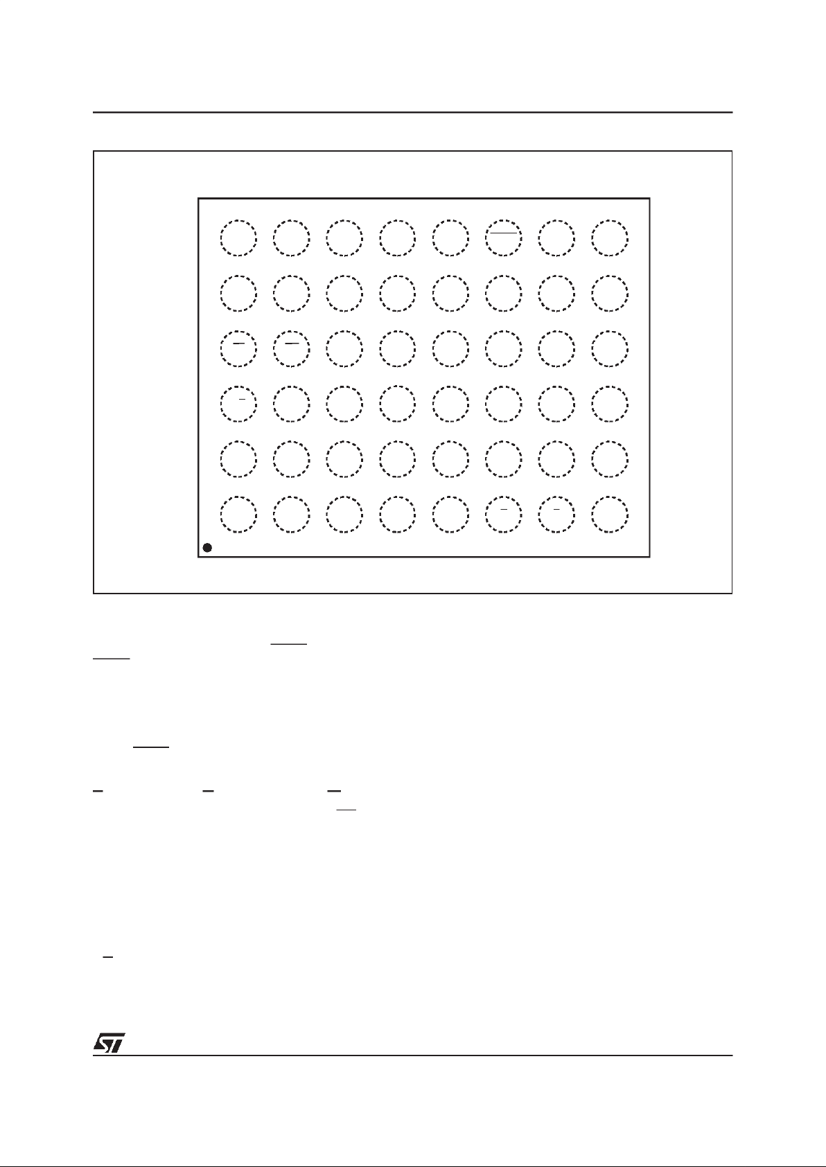
Figure 2. TSOP Connections
DQ3
DQ9
DQ2
A6
DQ0
W
A3
RB
DQ6
A8
A9
DQ13
A17
A10 DQ14
A2
DQ12
DQ10
DQ15A–1
V
CC
DQ4
DQ5
A7
DQ7
NC
NC
AI02179
M29W800T
M29W800B
12
1
13
24 25
36
37
48
DQ8
NC
NC
A1
A18
A4
A5
DQ1
DQ11
G
A12
A13
A16
A11
BYTE
A15
A14
V
SS
E
A0
RP
V
SS
Figure 3. SO Connections
G
DQ0
DQ8
A3
A0
E
V
SS
A2
A1
A13
V
SS
A14
A15
DQ7
A12
A16
BYTE
DQ15A–1
DQ5DQ2
DQ3
V
CC
DQ11
DQ4
DQ14
A9
W
RB
A4
RP
A7
AI02181
M29W800
T
M29W800B
8
2
3
4
5
6
7
9
10
11
12
13
14
15
16
32
31
30
29
28
27
26
25
24
2322
20
19
18
17DQ1
DQ9
A6
A5
DQ6
DQ13
44
39
38
37
36
35
34
33
A11
A10
DQ10
21
DQ12
40
43
1
42
41
A17 A8
A18
Table 1. Signal Names
A0-A18 Address Inputs
DQ0-DQ7 Data Input/Outputs, Command Inputs
DQ8-DQ14 Data Input/Outputs
DQ15A–1 Data Input/Output or Address Input
E Chip Enable
G Output Enable
W Write Enable
RP Reset/Block Temporary Unprotect
RB Ready/Busy Output
BYTE Byte/Word Organization
V
CC
Supply Voltage
V
SS
Ground
NC Not Connected Internally
DU Don’t Use as Internally Connected
DESCRIPTION
TheM29W800A isa non-volatile memory that may
be erased electrically at the blockor chiplevel and
programmed in-system on a Byte-by-Byte or
Word-by-Word basis using only a single 2.7V to
3.6V VCCsupply. For Program and Erase operations the necessary high voltages are generated
internally. The device can also be programmed in
standard programmers.
The array matrix organisation allowseach block to
be erased and reprogrammed without affecting
other blocks. Blocks can be protected against programing and erase on programming equipment,
and temporarily unprotected to make changes in
the application. Each block can be programmed
and erased over 100,000 cycles.
Instructions for Read/Reset, Auto Select for reading the Electronic Signature or Block Protection
status, Programming, Block and Chip Erase,
Erase Suspend and Resume are written to the device in cycles of commands to a Command Interface using standardmicroprocessor write timings.
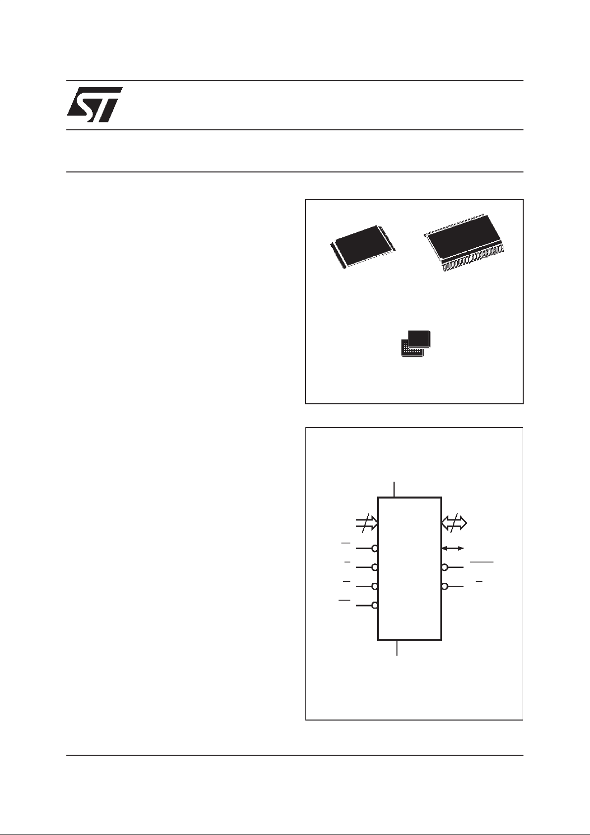
The device is offered in TSOP48 (12 x 20mm),
SO44 and LFBGA48 0.8 mm ball pitch packages.
3/33
M29W800AT, M29W800AB
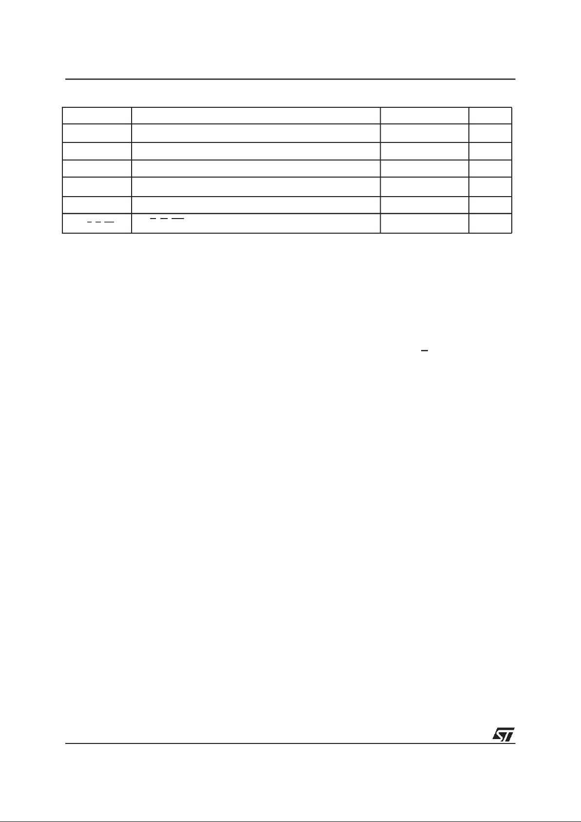
Figure 4. LFBGA Connections (Top view through package)
AI00656
D
E
F
87654321
B
C
A
V
SS
DQ15
A–1
A15A14A12A13
DQ3DQ11DQ10A18DURB
DQ1DQ9DQ8DQ0A6A17A7
GEA0 A4A3
DQ2
DQ6DQ13DQ14A10A8A9
DQ4V
CC
DQ12DQ5DUDURPW
A11 DQ7
A1 A2 V
SS
A5
DU
A16
BYTE
Memory Blocks
The devices featureasymmetrically blocked architecture providing system memoryintegration. Both
M29W800AT and M29W800AB devices have an
array of19blocks, one Boot Blockof 16KBytes or
8 KWords, two Parameter Blocks of 8 KBytes or 4
KWords, one Main Block of 32 KBytes or 16
KWords and fifteen Main Blocks of 64 KBytes or
32 KWords. The M29W800AT has the Boot Block
at the top of the memory address space and the
M29W800AB locates the Boot Block startingat the
bottom. The memory maps are showed in Figure
5.
Each block can be erased separately, any combi-
nation of blocks can be specified for multi-block
erase or theentirechip maybe erased. The Erase
operations are managed automatically by the P/
E.C. The block erase operation canbe suspended
in order to read from or program to any block not
being erased,and then resumed.
Block protection provides additional data security.
Each block can be separately protected or unprotected against Program or Erase on programming
equipment. All previously protected blocks can be
temporarily unprotected in the application.
Organisation
The M29W800A is organised as 1M x8 or 512K
x16 bits selectable by the BYTE signal. When
BYTE is Low the Byte-wide x8 organisation is selected and the address lines are DQ15A–1 and
A0-A18. The Data Input/Output signal DQ15A–1
acts as address line A–1 which selects the lower
or upper Byte of the memory word for output on
DQ0-DQ7, DQ8-DQ14remain at High impedance.
When BYTE isHigh the memory uses the address
inputs A0-A18 and the Data Input/Outputs DQ0DQ15. Memorycontrol isprovided by ChipEnable
E, Output Enable G and Write Enable W inputs.
A Reset/Block Temporary Unprotection RP tri-level input provides a hardware reset when pulled
Low, and when held High (at VID) temporarily unprotects blocks previously protected allowingthem
to be programed and erased. Erase and Program
operations are controlled by an internal Program/
Erase Controller (P/E.C.). Status Register data
output onDQ7 providesa Data Polling signal, and
DQ6 and DQ2 provide Toggle signals to indicate
the state of the P/E.C operations. A Ready/Busy
RB output indicates the completion of the internal
algorithms.
M29W800AT, M29W800AB
4/33
Bus Operations
The following operations can be performed using
the appropriate buscycles: Read (Array, Electronic Signature, Block Protection Status), Write command, Output Disable, Stan-by, Reset, Block
Protection, Unprotection,Protection Verify, Unprotection Verify and Block Temporary Unprotection.
See Tables 5and 6.
Command Interface
Instructions, made up of commands written in cycles, can begiven to the Program/Erase Controller
through a Command Interface (C.I.). For added
data protection,program orerase execution starts
after 4 or 6 cycles. The first, second, fourth and
fifth cycles are used to input Coded cycles to the
C.I. This Coded sequence is the same for all Program/Erase Controller instructions. The ’Command’ itself and its confirmation,when applicable,
are given on the third, fourth or sixth cycles. Any
incorrect commandor anyimproper command sequence will reset the device to Read Array mode.
Instructions
Seven instructions are defined to perform Read
Array, Auto Select (to read the Electronic Signature or Block Protection Status), Program, Block
Erase, ChipErase, Erase Suspend and EraseResume.
The internal P/E.C. automatically handles all timing and verification of the Program and Erase operations. The Status Register Data Polling,
Toggle, Error bits and the RB output may be read
at any time, during programmingor erase, tomonitor the progress of the operation.
Instructions are composed of up to six cycles. The
first two cycles input a Coded sequence to the
Command Interface which is common to all instructions (see Table 9).
The third cycle inputs the instruction set-up command. Subsequent cycles output the addressed
data, Electronic Signatureor Block Protection Status for Read operations. Inorder to give additional
data protection, the instructions for Program and
Block or Chip Erase require further command inputs. For a Program instruction, the fourth command cycle inputs the address and data to be
programmed. For an Erase instruction (Block or
Chip), the fourth and fifth cycles input a further
Coded sequence before the Erase confirm command on the sixth cycle. Erasure of a memory
block may be suspended, in order to read data
from another block or to program data in another
block, and then resumed. When power is first applied or if VCCfalls below V
LKO
, the command in-
terface is reset to Read Array.
Table 2. Absolute Maximum Ratings
(1)
Note: 1. Except for the rating ”Operating Temperature Range”, stresses above those listed in the Table ”Absolute Maximum Ratings” may
cause permanent damage to the device. These are stress ratings only and operation of the device at these or any other conditions
above those indicated in the Operating sections of this specification is not implied. Exposure to Absolute Maximum Rating conditions forextended periods mayaffect device reliability. Referalso to theSTMicroelectronics SURE Program and other relevantquality documents.
2. Minimum Voltage may undershoot to –2V during transition and for less than 20ns during transitions.
3. Depends on range.
Symbol Parameter Value Unit
T
A
Ambient Operating Temperature
(3)
–40 to 85 °C
T
BIAS
Temperature Under Bias –50 to 125 °C
T
STG
Storage Temperature –65 to 150 °C
V
IO
(2)
Input or Output Voltage –0.6 to 5 V
V
CC
Supply Voltage –0.6 to 5 V
V
(A9, E, G, RP)
(2)
A9, E, G, RP Voltage –0.6 to 13.5 V
5/33
M29W800AT, M29W800AB
Table 3. Top Boot Block Addresses,
M29W800AT
#
Size
(Kbytes)
Address Range
(x8)
Address Range
(x16)
18 16 FC000h-FFFFFh 7E000h-7FFFFh
17 8 FA000h-FBFFFh 7D000h-7DFFFh
16 8 F8000h-F9FFFh 7C000h-7CFFFh
15 32 F0000h-F7FFFh 78000h-7BFFFh
14 64 E0000h-EFFFFh 70000h-77FFFh
13 64 D0000h-DFFFFh 68000h-6FFFFh
12 64 C0000h-CFFFFh 60000h-67FFFh
11 64 B0000h-BFFFFh 58000h-5FFFFh
10 64 A0000h-AFFFFh 50000h-57FFFh
9 64 90000h-9FFFFh 48000h-4FFFFh
8 64 80000h-8FFFFh 40000h-47FFFh
7 64 70000h-7FFFFh 38000h-3FFFFh
6 64 60000h-6FFFFh 30000h-37FFFh
5 64 50000h-5FFFFh 28000h-2FFFFh
4 64 40000h-4FFFFh 20000h-27FFFh
3 64 30000h-3FFFFh 18000h-1FFFFh
2 64 20000h-2FFFFh 10000h-17FFFh
1 64 10000h-1FFFFh 08000h-0FFFFh
0 64 00000h-0FFFFh 00000h-07FFFh
Table 4. Bottom Boot Block Addresses,
M29W800AB
#
Size
(Kbytes)
Address Range
(x8)
Address Range
(x16)
18 64 F0000h-FFFFFh 78000h-7FFFFh
17 64 E0000h-EFFFFh 70000h-77FFFh
16 64 D0000h-DFFFFh 68000h-6FFFFh
15 64 C0000h-CFFFFh 60000h-67FFFh
14 64 B0000h-BFFFFh 58000h-5FFFFh
13 64 A0000h-AFFFFh 50000h-57FFFh
12 64 90000h-9FFFFh 48000h-4FFFFh
11 64 80000h-8FFFFh 40000h-47FFFh
10 64 70000h-7FFFFh 38000h-3FFFFh
9 64 60000h-6FFFFh 30000h-37FFFh
8 64 50000h-5FFFFh 28000h-2FFFFh
7 64 40000h-4FFFFh 20000h-27FFFh
6 64 30000h-3FFFFh 18000h-1FFFFh
5 64 20000h-2FFFFh 10000h-17FFFh
4 64 10000h-1FFFFh 08000h-0FFFFh
3 32 08000h-0FFFFh 04000h-07FFFh
2 8 06000h-07FFFh 03000h-03FFFh
1 8 04000h-05FFFh 02000h-02FFFh
0 16 00000h-03FFFh 00000h-01FFFh

M29W800AT, M29W800AB
6/33
SIGNAL DESCRIPTIONS
See Figure 1 and Table 1.
Address Inputs (A0-A18). The address inputs
for thememory arrayarelatched duringa writeoperation on the falling edge at Chip Enable E or
Write Enable W. In Word-wide organisation the
address lines are A0-A18, in Byte-wide organisation DQ15A–1 acts as an additional LSB address
line. WhenA9 is raised to VID, eithera Read Electronic Signature Manufacturer or Device Code,
Block Protection Status ora Write BlockProtection
or BlockUnprotection isenableddepending on the
combination oflevels on A0, A1,A6, A12andA15.
Data Input/Outputs (DQ0-DQ7). These Inputs/
Outputs are used in theByte-wide and Word-wide
organisations. Theinput isdata to beprogrammed
in the memory array ora command tobe written to
the C.I.Both are latched onthe rising edge ofChip
Enable E or Write Enable W. The output is data
from the Memory Array, the Electronic Signature
Manufacturer or Device codes, the Block Protection Status or the Status register Data Polling bit
DQ7, the Toggle Bits DQ6 and DQ2, the Error bit
DQ5 ortheErase Timer bitDQ3. Outputs arevalid
when Chip Enable E andOutput Enable G are active. The output is high impedance when the chip
is deselected or the outputs are disabled and
when RP isat a Low level.
Data Input/Outputs (DQ8-DQ14 and DQ15A–
1). These Inputs/Outputs are additionally used in
the Word-wide organisation. When BYTE is High
DQ8-DQ14 and DQ15A–1 act as the MSB of the
Data Input or Output, functioning as described for
DQ0-DQ7 above, and DQ8-DQ15 are ’don’t care’
for command inputs or status outputs. When
BYTE is Low, DQ0-DQ14 are high impedance,
DQ15A–1 is the Address A–1 input.
Chip Enable (E). The Chip Enable input activates the memory control logic, input buffers, decoders andsense amplifiers.E Highdeselects the
memory and reduces the power consumption to
the stan-by level. E can also be used to control
writing to the command register and to the memory array, while W remains at a low level. The Chip
Enable must be forcedto VIDduring the Block Unprotection operation.
Output Enable (G). The Output Enable gates the
outputs through the data buffersduring a read operation. When G is High the outputs are High impedance. G must be forced to VIDlevel during
Block Protection and Unprotection operations.
Write Enable (W). This input controls writing to
the Command Register and Address and Data
latches.
Byte/WordOrganizationSelect (BYTE). The BYTE
input selects the output configuration for the device: Byte-wide (x8) mode or Word-wide (x16)
mode. When BYTE is Low, the Byte-wide mode is
selected andthe data is read and programmed on
DQ0-DQ7. In this mode, DQ8-DQ14 are at high
impedance and DQ15A–1 is the LSB address.
When BYTE is High, the Word-wide mode is selected and the data is read and programmed on
DQ0-DQ15.
Ready/Busy Output (RB). Ready/Busy is an
open-drain output and gives the internal state of
the P/E.C. of thedevice. When RB is Low, the device is Busy with a Program or Erase operation
and it will not accept any additional program or
erase instructions except the Erase Suspend instruction. WhenRB is High,the deviceis ready for
any Read, Program or Erase operation. The RB
will also be Highwhen the memory is put in Erase
Suspend or Stan-by modes.
Reset/Block Temporary Unprotect Input (RP).
The RP Input provides hardware reset and protected block(s) temporary unprotection functions.
Reset of the memory is achieved by pulling RP to
VILfor at least t
PLPX
. When the reset pulse is given, if the memory is in Read or Stan-by modes, it
will be available for new operations in t
PHEL
after
the rising edge of RP. If the memory is in Erase,
Erase Suspend or Program modes the reset will
take t
PLYH
during which the RB signal will be held
at VIL. Theend of thememory reset will be indicated by the rising edge of RB. A hardware reset during an Erase or Program operation will corrupt the
data being programmed or the sector(s) being
erased. See Tables 15, 16, and Figure 11.
Temporary block unprotection is made by holding
RP at VID. In this condition previously protected
blocks can be programmed or erased. The transition of RP from VIHto VIDmust slower than t
PH-
PHH
. See Tables 17, 18, and Figure 11. When RP
is returned from VIDto VIHall blocks temporarily
unprotected will be again protected.
VCCSupply Voltage. The power supply for all
operations (Read, Program and Erase).
VSSGround. VSSis the reference for all voltage
measurements.

7/33
M29W800AT, M29W800AB
DEVICE OPERATIONS
See Tables 5, 6 and 7.
Read. Read operations are used to output the
contents of the Memory Array, the Electronic Signature, theStatus Register or the BlockProtection
Status. Both Chip Enable E and Output Enable G
must below in ordertoread theoutput of the memory. A new operation is initiated either on the following edge of Chip Enable E or on any address
transition with E at VIL.
Write. Write operations are used to give Instruction Commands to the memory or to latch input
data to be programmed. A write operation is initiated whenChip Enable E isLow and Write Enable
W is Low with Output Enable G High. Addresses
are latchedon the falling edgeof W orEwhichever
occurs last. Commands and Input Data are
latched onthe rising edgeof Wor Ewhicheveroccurs first.
Output Disable. The data outputs are high impedance when the Output Enable G is High with
Write Enable W High.
Stan-by. The memory is in stan-by when Chip
Enable E isHigh and the P/E.C. is idle. The power
consumption is reduced to the stan-by level and
the outputs are high impedance, independent of
the Output Enable G or Write Enable Winputs.
Automatic Stan-by. After 150ns of bus inactivity
(no addresstransition, CE=VIL) andwhen CMOS
levels aredriving theaddresses, the chip automatically enters a pseudo-stan-by mode where consumption is reduced to the CMOS stan-by value,
while outputs stilldrive the bus (if G = VIL).
Electronic Signature. Two codes identifying the
manufacturer andthe devicecan beread from the
memory. The manufacturer’s code for STMicroelectronics is 20h, the device code is D7h for the
M29W800AT (Top Boot) and 5Bh for the
M29W800AB (Bottom Boot). These codes allow
programming equipment or applications to automatically match their interface to the characteristics ofthe M29W800A. TheElectronic Signature is
output by a Read operation when the voltage applied to A9 is at VIDandaddress inputs A1 isLow.
The manufacturer code is output when the Address input A0 is Low and the device code when
this input is High. Other Address inputs are ignored. The codes are output on DQ0-DQ7.
The Electronic Signature canalso be read, without
raising A9 to VID, by giving the memory the Instruction AS. If the Byte-wide configuration is selected the codes are output on DQ0-DQ7 with
DQ8-DQ14 at High impedance; if the Word-wide
configuration is selected the codes are output on
DQ0-DQ7 withDQ8-DQ15 at 00h.
Block Protection. Each block can be separately
protected against Program or Erase on programming equipment. Block protection provides additional data security, as it disables all program or
erase operations. This mode is activated when
both A9 and G are raised to VIDand anaddress in
the block is applied on A12-A18. Block protection
is initiated on theedge ofW fallingto VIL. Then after a delay of 100µs, the edge of W rising to V
IH
ends the protection operations. Block protection
verify is achieved by bringing G, E, A0 and A6 to
VILand A1 to VIH, while W is at VIHand A9 at VID.
Under these conditions, reading the data output
will yield 01h if the block defined by the inputs on
A12-A18 is protected. Any attempt to program or
erase a protected block will be ignored by the device.
Block Temporary Unprotection. Any previously
protected block can be temporarily unprotected in
order to change stored data. The temporary unprotection mode isactivatedby bringing RP toVID.
During the temporary unprotection mode the previously protected blocks are unprotected. A block
can beselected and data can bemodified by executing the Erase or Program instruction with the
RP signal held at VID. When RP is returned toVIH,
all the previously protected blocks are again protected.
Block Unprotection. All protected blocks can be
unprotected on programming equipment to allow
updating of bit contents. All blocks must first be
protected before theunprotection operation. Block
unprotection is activated when A9,G and E are at
VIDand A12, A15 at VIH. Unprotection is initiated
by the edge of W falling to VIL. After a delay of
10ms, the unprotection operation will end. Unprotection verify is achieved by bringing G and E to
VILwhileA0 is at VIL, A6and A1are at VIHandA9
remains at VID. In these conditions, reading the
output data willyield 00hif the block definedbythe
inputs A12-A18 has been successfully unprotected. Each block must be separately verified by giving its address in order to ensure that it has been
unprotected.
M29W800AT, M29W800AB
8/33
Table 5. User Bus Operations
(1)
Note: 1. X = VILor VIH.
2. Block Address must be given an A12-A18 bits.
3. See Table 7.
4. Operation performed on programming equipment.
Table 6. Read Electronic Signature (following AS instruction or with A9 = VID)
Table 7. Read Block Protection with AS Instruction
Operation E G W RP BYTE A0 A1 A6 A9 A12 A15
DQ0-
DQ7
DQ8-
DQ14
DQ15
A–1
Read Word
V
ILVIL
V
IH
V
IHVIH
A0 A1 A6 A9 A12 A15
Data
Output
Data
Output
Data
Output
Read Byte
V
ILVIL
V
IH
V
IH
V
IL
A0 A1 A6 A9 A12 A15
Data
Output
Hi-Z
Address
Input
Write Word
V
ILVIH
V
IL
V
IHVIH
A0 A1 A6 A9 A12 A15
Data
Input
Data
Input
Data
Input
Write Byte
V
ILVIH
V
IL
V
IH
V
IL
A0 A1 A6 A9 A12 A15
Data
Input
Hi-Z
Address
Input
Output Disable
V
ILVIH
V
IH
V
IH
X XXXX X X Hi-Z Hi-Z Hi-Z
Stan-by
V
IH
XX
V
IH
X XXXX X X Hi-Z Hi-Z Hi-Z
Reset X X X
V
IL
X XXXX X X Hi-Z Hi-Z Hi-Z
Block
Protection
(2,4)
VILVIDVILPulse V
IH
X XXX
V
ID
XX X X X
Blocks
Unprotection
(4)
VIDVIDVILPulse V
IH
X XXX
V
IDVIHVIH
XXX
Block
Protection
Verify
(2,4)
VILV
IL
V
IH
V
IH
X
V
ILVIHVILVID
A12 A15
Block
Protect
Status
(3)
XX
Block
Unprotection
Verify
(2,4)
VILV
IL
V
IH
V
IH
X
V
ILVIHVIHVID
A12 A15
Block
Protect
Status
(3)
XX
Block
Temporary
Unprotection
XX X
V
ID
X XXXX X X X X X
Org. Code Device E G W BYTE A0 A1
Other
Addresses
DQ0-
DQ7
DQ8-
DQ14
DQ15
A–1
Word-
wide
Manufact.
Code
V
IL
V
IL
V
IH
V
IH
V
IL
V
IL
Don’t Care 20h 00h 0
Device
Code
M29W800AT
V
IL
V
IL
V
IH
V
IH
V
IH
V
IL
Don’t Care D7h 00h 0
M29W800AB
V
IL
V
IL
V
IH
V
IH
V
IH
V
IL
Don’t Care 5Bh 00h 0
Code E G W A0 A1 A12-A18
Other
Addresses
DQ0-DQ7
Protected Block
V
IL
V
IL
V
IH
V
IL
V
IH
Block Address Don’t Care 01h
Unprotected Block
V
IL
V
IL
V
IH
V
IL
V
IH
Block Address Don’t Care 00h
9/33
M29W800AT, M29W800AB
Table 8. Commands
Hex Code Command
00h Invalid/Reserved
10h Chip Erase Confirm
20h Reserved
30h Block Erase Resume/Confirm
80h Set-up Erase
90h
Read Electronic Signature/
Block Protection Status
A0h Program
B0h Erase Suspend
F0h Read Array/Reset
INSTRUCTIONS AND COMMANDS
The Command Interface latches commands written to the memory. Instructions are made up from
one or more commands to perform Read Memory
Array, Read Electronic Signature, ReadBlockProtection, Program, Block Erase, Chip Erase, Erase
Suspend and Erase Resume. Commands are
made of address and data sequences. The instructions requirefrom 1 to6 cycles,thefirst or first
three ofwhich are always write operations used to
initiate the instruction. They are followed by either
further writecycles to confirm the firstcommand or
execute thecommand immediately. Commandsequencing must be followed exactly. Any invalid
combination of commands will reset the device to
Read Array. The increased number of cycles has
been chosentoassuremaximum datasecurity. Instructions are initialised by twoinitialCodedcycles
which unlock the Command Interface. In addition,
for Erase,instructionconfirmation is again preceded by the two Coded cycles.
Status Register Bits
P/E.C. statusis indicated during executionby Data
Polling on DQ7, detection of Toggle on DQ6 and
DQ2, or Error on DQ5 and Erase Timer DQ3 bits.
Any read attempt during Program or Erase command execution will automatically output these
five Status Registerbits. The P/E.C. automatically
sets bits DQ2, DQ3, DQ5, DQ6 and DQ7. Other
bits (DQ0, DQ1 and DQ4) are reserved for future
use and should be masked. See Tables10 and11.
Data Polling Bit (DQ7). When Programming operations are in progress, this bit outputs the complement of the bit being programmed on DQ7.
During Erase operation, it outputsa ’0’. After completion ofthe operation, DQ7 will outputthebit last
programmed or a ’1’ after erasing. Data Polling is
valid and only effective during P/E.C. operation,
that is after the fourth W pulse for programming or
after the sixth W pulse for erase. It must be performed at the address beingprogrammed or at an
address within the block being erased. If all the
blocks selectedfor erasureare protected, DQ7 will
be set to ’0’for about 100µs, and then return to the
previous addressed memory data value. See Figure 13for the Data Polling flowchartand Figure 12
for the Data Polling waveforms. DQ7 will also flag
the Erase Suspend mode by switching from ’0’ to
’1’ at the start of the Erase Suspend. In order to
monitor DQ7 in the Erase Suspend mode an address within a block being erased must be provided. For a Read Operation in Erase Suspend
mode, DQ7 will output ’1’ if the read is attempted
on a block being erased and thedata value onother blocks. DuringProgramoperation in EraseSuspend Mode, DQ7 will have the same behavior as
in the normal program execution outside of the
suspend mode.
Toggle Bit (DQ6). When Programming or Erasing operations are in progress, successive attempts to read DQ6 will output complementary
data. DQ6 will togglefollowing toggling ofeither G,
or E when G is low. The operation is completed
when two successive reads yield the same output
data. The next read will output the bit last programmed ora ’1’ after erasing. The toggle bitDQ6
is valid only during P/E.C. operations, that is after
the fourth W pulse for programming or after the
sixth W pulse for Erase. If the blocks selected for
erasure are protected, DQ6 will toggle for about
100µs and then return back to Read. DQ6 will be
set to ’1’ if a Read operation is attempted on an
Erase Suspend block. When erase is suspended
DQ6 will toggle during programming operations in
a block differentto the blockin Erase Suspend. Either E or G toggling will cause DQ6 to toggle. See
Figure 14 for Toggle Bit flowchart and Figure 15
for Toggle Bit waveforms.
M29W800AT, M29W800AB
10/33
Table 9. Instructions
(1)
Note: 1. Commands not interpreted in this table will default to read array mode.
2. A wait of t
PLYH
is necessary after a Read/Reset command if the memory was in an Erase or Program mode before starting anynew
operation (see Tables 15, 16 and Figure 11).
3. X = Don’t Care.
4. The first cycles of the RD or AS instructions are followed by read operations. Any number of read cycles can occur after the command cycles.
5. Signature Address bits A0, A1, at V
IL
will output Manufacturer code (20h). Address bits A0 at VIHand A1, at VILwilloutput Device
code.
6. Block Protection Address: A0, at V
IL
,A1atVIHand A15-A18 within the Block will output the Block Protection status.
7. For Coded cycles address inputs A11-A18 aredon’t care.
8. Optional, additional Blocks addresses must be entered within the erase timeout delay after last write entry, timeout statuscan be
verified through DQ3 value (see Erase Timer Bit DQ3 description). When full command isentered, read Data Polling or Toggle bit
until Erase is completed or suspended.
9. Read Data Polling, Toggle bits or RB until Erase completes.
10. During Erase Suspend, Read and Data Program functions are allowed in blocks not being erased.
Mne. Instr. Cyc. 1st Cyc. 2nd Cyc. 3rd Cyc. 4th Cyc. 5th Cyc. 6th Cyc. 7th Cyc.
RD
(2,4)
Read/Reset
Memory Array
1+
Addr.
(3,7)
X Read Memory Array until anew write cycle is initiated.
Data F0h
3+
Addr.
(3,7)
Byte AAAh 555h AAAh
Read Memory Array until a new write cycle is
initiated.
Word 555h 2AAh 555h
Data AAh 55h F0h
AS
(4)
Auto Select 3+
Addr.
(3,7)
Byte AAAh 555h AAAh
Read Electronic Signature or Block Protection
Status until anew write cycle isinitiated. See Note
5 and 6.
Word 555h 2AAh 555h
Data AAh 55h 90h
PG Program 4
Addr.
(3,7)
Byte AAAh 555h AAAh
Program
Address
Read Data Polling or ToggleBit until
Program completes.
Word 555h 2AAh 555h
Data AAh 55h A0h
Program
Data
BE Block Erase 6
Addr.
(3,7)
Byte AAAh 555h AAAh AAAh 555h
Block
Address
Additional
Block
(8)
Word 555h 2AAh 555h 555h 2AAh
Data AAh 55h 80h AAh 55h 30h 30h
CE Chip Erase 6
Addr.
(3,7)
Byte AAAh 555h AAAh AAAh 555h AAAh
Note 9Word 555h 2AAh 555h 555h 2AAh 555h
Data AAh 55h 80h AAh 55h 10h
ES
(10)
Erase
Suspend
1
Addr.
(3,7)
X
Read until Togglestops, then read all the data needed from any Block(s)
not being erased then Resume Erase.
Data B0h
ER
Erase
Resume
1
Addr.
(3,7)
X
Read Data Polling or Toggle Bits until Erase completes or Erase is
suspended another time.
Data 30h

11/33
M29W800AT, M29W800AB
Table 10. Status Register Bits
Note: Logic level ’1’ is High, ’0’ is Low. -0-1-0-0-0-1-1-1-0- represent bit value in successive Read operations.
DQ Name Logic Level Definition Note
7
Data
Polling
’1’
Erase Complete or erase block
in Erase Suspend
Indicates the P/E.C. status, check during
Program orErase, and on completion before
checking bits DQ5 for program or Erase
Success.
’0’ Erase On-going
DQ
Program Complete or data of
non erase block during Erase
Suspend
DQ Program On-going
6 Toggle Bit
’-1-0-1-0-1-0-1-’ Erase or Program On-going
Successive reads output complementary
data on DQ6 while Programming or Erase
operations are on-going. DQ6 remains at
constant levelwhen P/E.C. operations are
completed or Erase Suspend is
acknowledged.
DQ Program Complete
’-1-1-1-1-1-1-1-’
Erase Complete or Erase
Suspend on currently
addressed block
5 Error Bit
’1’ Program or Erase Error
This bit is set to ‘1’ in the case of
Programming or Erase failure.
’0’ Program or Erase On-going
4 Reserved
3
Erase
Time Bit
’1’ Erase Timeout Period Expired
P/E.C. Erase operation has started. Only
possible command entry is Erase Suspend
(ES).
’0’ Erase Timeout Period On-going
An additional block to be erased in parallel
can be entered to the P/E.C.
2 Toggle Bit
’-1-0-1-0-1-0-1-’
Chip Erase, Erase or Erase
Suspend on the currently
addressed block.
Erase Errordue to thecurrently
addressed block
(when DQ5 = ‘1’).
Indicates the erase status and allows to
identify the erased block
1
Program on-going, Erase ongoing on another block or
Erase Complete
DQ
Erase Suspend read on non
Erase Suspend block
1 Reserved
0 Reserved

M29W800AT, M29W800AB
12/33
During the second cycle theCoded cycles consist
ofwriting the data55h ataddress555h inthe Bytewide configuration and at address 2AAh in the
Word-wide configuration. In the Byte-wide configuration the address lines A–1 to A10 are valid, in
Word-wide A0 to A11are valid,otheraddress lines
are ’don’t care’. The Coded cycles happen on first
and second cyclesof the command write or on the
fourth and fifth cycles.
Instructions
See Table9.
Read/Reset (RD) Instruction. The Read/Reset
instruction consists of one write cycle giving the
command F0h. It can be optionally preceded by
the two Coded cycles. Subsequent read operations will read the memory array addressed and
output the data read. A wait state of 10µs is necessary after Read/Reset prior to any valid read if
the memory was in an Erase mode when the RD
instruction is given. The Read/Reset command is
not accepted during Erase and erase Suspend.
Auto Select (AS) Instruction. This instruction
uses the two Coded cycles followed by one write
cycle giving thecommand 90hto address AAAh in
the Byte-wide configurationor address 555hinthe
Word-wide configuration for command set-up. A
subsequent read will output the manufacturer
code and the device code or the block protection
status depending on the levels of A0 and A1. The
manufacturer code, 20h, is output when the addresses lines A0and A1are Low,thedevice code,
EEh for Top Boot, EFh for Bottom Boot is output
when A0 is High with A1 Low.
The AS instruction also allows access tothe block
protection status. After giving the AS instruction,
A0 is set to VILwith A1 at VIH, while A12-A18 define the address of the block to be verified.A read
in these conditions will output a 01h if the block is
protected and a 00h if the block is not protected.
Program (PG)Instruction. This instruction uses
four write cycles. Both for Byte-wide configuration
and for Word-wide configuration. The Program
command A0h is written to address AAAh in the
Byte-wide configuration or to address 555h in the
Word-wide configuration on the third cycle after
two Coded cycles. A fourth write operation latches
the Addresson the falling edge of W or E and the
Data to bewritten on therising edge and starts the
P/E.C. Read operations outputtheStatus Register
bits after the programming has started. Memory
programming is madeonly by writing ’0’in place of
’1’. Status bits DQ6 and DQ7 determine if programming ison-going and DQ5 allows verification
of any possible error. Programming at an address
not in blocks being erased is also possible during
erase suspend. In this case, DQ2 will toggle at the
address being programmed.
Table 11. Polling and Toggle Bits
Note: 1. Toggle ifthe address iswithin a block being erased.
’1’if the address is within a block not being erased.
Mode DQ7 DQ6 DQ2
Program DQ7 Toggle 1
Erase 0 Toggle Note 1
Erase Suspend Read
(in Erase Suspend
block)
1 1 Toggle
Erase Suspend Read
(outside Erase Suspend
block)
DQ7 DQ6 DQ2
Erase Suspend Program DQ7 Toggle N/A
Toggle Bit (DQ2). This toggle bit, together with
DQ6, can be used to determine the device status
during theErase operations. Itcan alsobe used to
identify the block being erased. During Erase or
Erase Suspend a read from a block being erased
will cause DQ2 to toggle. A read from a block not
being erased will set DQ2 to ’1’ during erase and
to DQ2 during Erase Suspend. During Chip Erase
a read operation will cause DQ2 to toggle as all
blocks arebeing erased. DQ2 willbe set to’1’during program operation and when erase is complete. After erase completion and if the error bit
DQ5 is set to ’1’,DQ2 will toggleif the faulty block
is addressed.
Error Bit (DQ5). This bit is set to ’1’ by the P/E.C.
when there is a failure of programming, block
erase, or chip erase that results in invalid data in
the memory block. In case of an error in block
erase or program, the block in which the error occurred or to which the programmed data belongs,
must be discarded. The DQ5 failure condition will
also appear if a user tries to program a ’1’ to a location that is previously programmed to ’0’. Other
Blocks may still beused. The errorbit resets after
a Read/Reset(RD) instruction. In caseof success
of Program or Erase, the error bit will be set to ’0’.
Erase Timer Bit(DQ3). This bit is set to ’0’by the
P/E.C. when the last block Erase command has
been entered to the Command Interface and it is
awaiting the Erase start. When the erase timeout
period is finished, after 50µsto90µs, DQ3 returns
to ’1’.
Coded Cycles
The two Coded cycles unlock theCommand Interface. Theyare followedby an input command or a
confirmation command. The Coded cycles consist
of writing the data AAh at address AAAh in the
Byte-wide configuration and at address 555h in
the Word-wide configuration during the first cycle.

13/33
M29W800AT, M29W800AB
Figure 5. AC Testing Input Output Waveform
AI01417
3V
0V
1.5V
Figure 6. AC Testing Load Circuit
AI01968
0.8V
OUT
CL= 30pF or 100pF
CLincludes JIG capacitance
3.3kΩ
1N914
DEVICE
UNDER
TEST
Table 13. Capacitance
(1)
(TA=25°C, f = 1 MHz)
Note: Sampled only, not 100% tested.
Table 14. DC Characteristics
(TA= 0 to 70°C, –20 to 85°C or –40 to 85°C; VCC= 2.7V to 3.6V)
Note: 1. Sampled only, not 100% tested.
Symbol Parameter Test Condition Min Max Unit
C
IN
Input Capacitance
V
IN
=0V
6pF
C
OUT
Output Capacitance
V
OUT
=0V
12 pF
Symbol Parameter Test Condition Min
Typ.
Max Unit
I
LI
Input Leakage Current
0V ≤ V
IN
≤ V
CC
±1
µA
I
LO
Output Leakage Current
0V ≤ V
OUT
≤ V
CC
±1 µA
I
CC1
Supply Current (Read by Word)
E=V
IL
,G=VIH,f=6MHz
310mA
I
CC2
Supply Current (Read by Word)
E=V
IL
,G=VIL, f = 6MHz
4.5 10 mA
I
CC3
Supply Current (Stan-by) E = VCC±0.2V 30 100 µA
I
CC4
(1)
Supply Current
(Program or Erase)
Byte program, Block or
Chip Erase in progress
20 mA
V
IL
Input Low Voltage –0.5 0.8 V
V
IH
Input High Voltage
0.7 V
CC
VCC+ 0.3
V
V
OL
Output Low Voltage
I
OL
= 1.8mA
0.45 V
V
OH
Output High Voltage CMOS
I
OH
= –100µAVCC–0.4V
V
V
ID
A9 Voltage(Electronic Signature) 11.5 12.5 V
I
ID
A9 Current (Electronic Signature)
A9 = V
ID
30 100 µA
V
LKO
(1)
Supply Voltage (Erase and
Program lock-out)
2.0 2.3 V
Table 12. AC Measurement Conditions
Input Rise and Fall Times ≤10ns
Input Pulse Voltages 0 to 3V
Input and Output Timing Ref. Voltages 1.5V

M29W800AT, M29W800AB
14/33
Table 15. Read AC Characteristics
(TA= 0 to 70°C, –20 to 85°C or –40 to 85°C)
Note: 1. Sampled only, not 100% tested.
2. G may be delayed byup to t
ELQV-tGLQV
after the falling edge of E without increasing t
ELQV
.
3. To be considered only if the Reset pulse is given while thememory is inErase or Program mode.
Symbol Alt Parameter
Test
Condition
M29W800AT / M29W800AB
Unit
80 90
V
CC
= 3.0V to 3.6V
CL = 30pF
VCC= 3.0V to 3.6V
CL = 30pF
Min Max Min Max
t
AVAV
t
RC
Address Validto Next
Address Valid
E=V
IL,
G=V
IL
80 90 ns
t
AVQV
t
ACC
Address Validto Output
Valid
E=V
IL,
G=V
IL
80 90 ns
t
AXQX
t
OH
Address Transition to
Output Transition
E=V
IL,
G=V
IL
00
ns
t
BHQV
t
FHQV
BYTE Switching High to
Output Valid
50 50 ns
t
BLQZ
t
FLQZ
BYTE Switching Low to
Output High Z
50 50 ns
t
EHQX
t
OH
Chip Enable High to Output
Transition
G=V
IL
00ns
t
EHQZ
(1)
t
HZ
Chip Enable High to Output
Hi-Z
G=V
IL
30 30 ns
t
ELBH
t
ELBL
t
ELFH
t
ELFL
Chip Enable to BYTE
Switching Low or High
55ns
t
ELQV
(2)
t
CE
Chip Enable Low to Output
Valid
G=V
IL
80 90 ns
t
ELQX
(1)
t
LZ
Chip Enable Low to Output
Transition
G=V
IL
00ns
t
GHQX
t
OH
Output Enable High to
Output Transition
E=V
IL
00ns
t
GHQZ
(1)
t
DF
Output Enable High to
Output Hi-Z
E=V
IL
30 30 ns
t
GLQV
(2)
t
OE
Output Enable Lowto
Output Valid
E=V
IL
35 35 ns
t
GLQX
(1)
t
OLZ
Output Enable Lowto
Output Transition
E=V
IL
00ns
t
PHEL
t
RH
RP High to Chip Enable
Low
50 50 ns
t
PLYH
(1, 3)
t
RRB
t
READY
RP Low to Read Mode 10 10 µs
t
PLPX
t
RP
RP Pulse Width 500 500 ns

15/33
M29W800AT, M29W800AB
Table 16. Read AC Characteristics
(TA= 0 to 70°C, –20 to 85°C or –40 to 85°C)
Note: 1. Sampled only, not 100% tested.
2. G may be delayed byup to t
ELQV-tGLQV
after the falling edge of E without increasing t
ELQV
.
3. To be considered only if the Reset pulse is given while thememory is inErase or Program mode.
Symbol Alt Parameter
Test
Condition
M29W800AT / M29W800AB
Unit
100 120
V
CC
= 2.7V to 3.6V
CL = 30pF
VCC= 2.7V to 3.6V
CL = 30pF
Min Max Min Max
t
AVAV
t
RC
Address Validto Next
Address Valid
E=V
IL,
G=V
IL
100 120 ns
t
AVQV
t
ACC
Address Validto Output
Valid
E=V
IL,
G=V
IL
100 120 ns
t
AXQX
t
OH
Address Transition to
Output Transition
E=V
IL,
G=V
IL
00
ns
t
BHQV
t
FHQV
BYTE Switching High to
Output Valid
50 60 ns
t
BLQZ
t
FLQZ
BYTE Switching Low to
Output High Z
50 60 ns
t
EHQX
t
OH
Chip Enable High to Output
Transition
G=V
IL
00ns
t
EHQZ
(1)
t
HZ
Chip Enable High to Output
Hi-Z
G=V
IL
30 30 ns
t
ELBH
t
ELBL
t
ELFH
t
ELFL
Chip Enable to BYTE
Switching Low or High
55ns
t
ELQV
(2)
t
CE
Chip Enable Low to Output
Valid
G=V
IL
100 120 ns
t
ELQX
(1)
t
LZ
Chip Enable Low to Output
Transition
G=V
IL
00ns
t
GHQX
t
OH
Output Enable High to
Output Transition
E=V
IL
00ns
t
GHQZ
(1)
t
DF
Output Enable High to
Output Hi-Z
E=V
IL
30 30 ns
t
GLQV
(2)
t
OE
Output Enable Lowto
Output Valid
E=V
IL
40 50 ns
t
GLQX
(1)
t
OLZ
Output Enable Lowto
Output Transition
E=V
IL
00ns
t
PHEL
t
RH
RP High to Chip Enable
Low
50 50 ns
t
PLYH
(1, 3)
t
RRB
t
READY
RP Low to Read Mode 10 10 µs
t
PLPX
t
RP
RP Pulse Width 500 500 ns

M29W800AT, M29W800AB
16/33
Figure 7. Read Mode AC Waveforms
AI02182
tAVAV
tAVQV tAXQX
tELQX tEHQX
tGLQV
tGLQX
tGHQX
VALID
A0-A18/
A–1
E
G
DQ0-DQ7/
DQ8-DQ15
tELQV
VALID
ADDRESS VALID
AND CHIP ENABLE
OUTPUT ENABLE DATA VALID
BYTE
tBLQZtELBL/tELBH
tEHQZ
tGHQZ
tBHQV
Note: Write Enable (W) = High.

17/33
M29W800AT, M29W800AB
Table 17. Write AC Characteristics, W Controlled
(TA= 0 to 70°C, –20 to 85°C or –40 to 85°C)
Note: 1. Sampled only, not 100% tested.
2. This timing is for Temporary Block Unprotection operation.
Symbol Alt Parameter
M29W800AT / M29W800AB
Unit
80 90
V
CC
= 3.0V to 3.6V
CL = 30pF
VCC= 3.0V to 3.6V
CL = 30pF
Min Max Min Max
t
AVAV
t
WC
Address Valid to Next Address Valid 80 90 ns
t
AVWL
t
AS
Address Valid to Write Enable Low 0 0 ns
t
DVWH
t
DS
Input Valid to Write Enable High 35 45 ns
t
ELWL
t
CS
Chip Enable Low to Write Enable Low 0 0 ns
t
GHWL
Output Enable High to Write Enable Low 0 0 ns
t
PHPHH
(1, 2)
t
VIDR
RP Rise Time to V
ID
500 500 ns
t
PHWL
(1)
t
RSP
RP High to Write Enable Low 4 4 µs
t
PLPX
t
RP
RP Pulse Width 500 500 ns
t
VCHEL
t
VCSVCC
High to Chip Enable Low
50 50 µs
t
WHDX
t
DH
Write Enable High to Input Transition 0 0 ns
t
WHEH
t
CH
Write Enable High to Chip Enable High 0 0 ns
t
WHGL
t
OEH
Write Enable High to Output Enable Low 0 0 ns
t
WHRL
(1)
t
BUSY
Program Erase Valid to RB Delay 90 90 ns
t
WHWL
t
WPH
Write Enable High to Write Enable Low 30 30 ns
t
WLAX
t
AH
Write Enable Low to Address Transition 45 45 ns
t
WLWH
t
WP
Write Enable Low to Write Enable High 35 35 ns
Block Erase (BE) Instruction. This instruction
uses a minimum of six write cycles. The Erase
Set-up command 80h is written to address AAAh
in the Byte-wide configuration or address 555h in
the Word-wide configuration on third cycle after
the two Coded cycles. The Block Erase Confirm
command 30h issimilarly written onthesixth cycle
after anothertwo Coded cycles.During theinput of
the second command an address within the block
to beerased is givenandlatched into the memory.
Additional block Erase Confirm commands and
block addresses can be written subsequently to
erase other blocks in parallel,without further Coded cycles. The erase will start after the erase timeout period (seeErase TimerBit DQ3description).
Thus, additional Erase Confirmcommandsforother blocks must begiven withinthisdelay.The input
of a new Erase Confirm command will restart the
timeout period. The status of the internal timer can
be monitored through thelevel of DQ3,if DQ3is ’0’
the Block Erase Command has been given and
the timeout is running, if DQ3 is ’1’, thetimeout has
expired and the P/E.C. is erasing the Block(s). If
the second command given is not an erase confirm or if the Coded cycles are wrong, the instruction aborts, and the device isreset to Read Array.
It is not necessary to program the block with 00h
as the P/E.C. will do this automatically before to
erasing to FFh. Read operations after thesixth rising edge ofW or E outputthe status registerstatus
bits.

M29W800AT, M29W800AB
18/33
Table 18. Write AC Characteristics, W Controlled
(TA= 0 to 70°C, –20 to 85°C or –40 to 85°C)
Note: 1. Sampled only, not 100% tested.
2. This timing is for Temporary Block Unprotection operation.
Symbol Alt Parameter
M29W800AT / M29W800AB
Unit
100 120
V
CC
= 2.7V to 3.6V
CL = 30pF
VCC= 2.7V to 3.6V
CL = 30pF
Min Max Min Max
t
AVAV
t
WC
Address Valid to Next Address Valid 100 120 ns
t
AVWL
t
AS
Address Valid to Write Enable Low 0 0 ns
t
DVWH
t
DS
Input Valid to Write Enable High 45 50 ns
t
ELWL
t
CS
Chip Enable Low to Write Enable Low 0 0 ns
t
GHWL
Output Enable High to Write Enable Low 0 0 ns
t
PHPHH
(1, 2)
t
VIDR
RP Rise Time to V
ID
500 500 ns
t
PHWL
(1)
t
RSP
RP High to Write Enable Low 4 4 µs
t
PLPX
t
RP
RP Pulse Width 500 500 ns
t
VCHEL
t
VCSVCC
High to Chip Enable Low
50 50 µs
t
WHDX
t
DH
Write Enable High to Input Transition 0 0 ns
t
WHEH
t
CH
Write Enable High to Chip Enable High 0 0 ns
t
WHGL
t
OEH
Write Enable High to Output Enable Low 0 0 ns
t
WHRL
(1)
t
BUSY
Program Erase Valid to RB Delay 90 90 ns
t
WHWL
t
WPH
Write Enable High to Write Enable Low 30 30 ns
t
WLAX
t
AH
Write Enable Low to Address Transition 45 50 ns
t
WLWH
t
WP
Write Enable Low to Write Enable High 35 50 ns
During the execution of the erase by the P/E.C.,
the memory accepts only the Erase Suspend ES
and Read/Reset RD instructions. Data Polling bit
DQ7 returns ’0’ while the erasure is in progress
and ’1’ whenit has completed. The Toggle bit DQ2
and DQ6 toggle during the erase operation. They
stop when erase is completed. After completion
the Status Register bit DQ5 returns ’1’ if there has
been anerasefailure. In such asituation, theToggle bit DQ2 can be used to determine whichblock
is notcorrectlyerased. Inthe case of erase failure,
a Read/ResetRD instructionis necessary in order
to reset the P/E.C.
Chip Erase (CE) Instruction. This instruction
uses sixwrite cycles. The Erase Set-up command
80h is written to address AAAh in the Byte-wide
configuration or the address 555h in the Word-
wide configuration on the third cycle after the two
Coded cycles. The Chip Erase Confirmcommand
10h is similarly written on the sixth cycle after another two Coded cycles. If the second command
given is not an erase confirm or if the Coded cycles are wrong, the instruction aborts and the device is reset to Read Array. It is not necessary to
program the array with 00h first as the P/E.C. will
automatically do this before erasing it to FFh.
Read operations afterthe sixthrising edge of W or
E output the Status Register bits. During the execution of the erase by the P/E.C., Data Polling bit
DQ7 returns ’0’,then ’1’oncompletion. TheToggle
bits DQ2 and DQ6 toggle during erase operation
and stop when erase is completed. After completion the Status Register bit DQ5 returns ’1’if there
has been an Erase Failure.

19/33
M29W800AT, M29W800AB
Figure 8. Write AC Waveforms, W Controlled
Note: Address are latched on the falling edge of W, Data is latched onthe rising edge of W.
AI02183
E
G
W
A0-A18/
A–1
DQ0-DQ7/
DQ8-DQ15
VALID
VALID
V
CC
tVCHEL
tWHEH
tWHWL
tELWL
tAVWL
tWHGL
tWLAX
tWHDX
tAVAV
tDVWH
tWLWHtGHWL
RB
tWHRL
Erase Suspend (ES)Instruction. The Block
Erase operation may be suspended by this instruction which consists of writing the command
B0h without any specific address. No Coded cycles are required. It permits reading of data from
another block and programming in another block
while anerase operationisin progress.Erase suspend is accepted only during the Block Erase instruction execution. Writing this command during
Erase timeout will, in addition to suspending the
erase, terminate the timeout. The Toggle bit DQ6
stops toggling when the P/E.C. is suspended. The
Toggle bits will stop toggling between 0.1µs and
15µs after the Erase Suspend (ES) command has
been written.The device will then automatically be
set to Read Memory Array mode. When erase is
suspended, a Read from blocks being erased will
output DQ2 toggling and DQ6 at ’1’.A Read from
a block notbeing erased returnsvalid data. During
suspension the memory will respond only to the
Erase Resume ER and the Program PG instructions. A Program operation can be initiated during
erase suspend in one of the blocks not being
erased. Itwill result inboth DQ2 and DQ6 toggling
when the data is being programmed. A Read/Reset command willdefinitively abort erasureand result in invalid data in the blocks being erased.
Erase Resume (ER) Instruction. If an Erase
Suspend instruction was previously executed, the
erase operation may be resumed by giving the
command 30h, at any address, and without any
Coded cycles.

M29W800AT, M29W800AB
20/33
Table 19. Write AC Characteristics, E Controlled
(TA= 0 to 70°C, –20 to 85°C or –40 to 85°C)
Note: 1. Sampled only, not 100% tested.
2. This timing is for Temporary Block Unprotection operation.
Symbol Alt Parameter
M29W800AT / M29W800AB
Unit
80 90
V
CC
= 3.0V to 3.6V
CL = 30pF
VCC= 3.0V to 3.6V
CL = 30pF
Min Max Min Max
t
AVAV
t
WC
Address Valid to Next Address Valid 80 90 ns
t
AVEL
t
AS
Address Valid to Chip Enable Low 0 0 ns
t
DVEH
t
DS
Input Valid to Chip Enable High 35 45 ns
t
EHDX
t
DH
Chip Enable High to Input Transition 0 0 ns
t
EHEL
t
CPH
Chip Enable High to Chip Enable Low 30 30 ns
t
EHGL
t
OEH
Chip Enable High to Output Enable Low 0 0 ns
t
EHRL
(1)
t
BUSY
Program Erase Valid to RB Delay 80 90 ns
t
EHWH
t
WH
Chip Enable High to Write Enable High 0 0 ns
t
ELAX
t
AH
Chip Enable Low to Address Transition 45 45 ns
t
ELEH
t
CP
Chip Enable Low to Chip Enable High 35 35 ns
t
GHEL
Output Enable High Chip Enable Low 0 0 ns
t
PHPHH
(1, 2)
t
VIDR
RP Rise TIme to V
ID
500 500 ns
t
PHWL
(1)
t
RSP
RP High to Write Enable Low 4 4 µs
t
PLPX
t
RP
RP Pulse Width 500 500 ns
t
VCHWL
t
VCSVCC
High to Write Enable Low
50 50 µs
t
WLEL
t
WS
Write Enable Low to Chip Enable Low 0 0 ns
POWER SUPPLY
Power Up
The memory Command Interface is reset on power up to Read Array. The device does not accept
commands on the first rising edge of W, if both W
and E are at VILwith G at VIHduring power-up.
Any write cycle initiation is blocked when VCCis
below V
LKO
.
Supply Rails
Normal precautions must be taken for supply voltage decoupling; each device in a system should
have the VCCrail decoupled with a 0.1µFcapacitor
close to the VCCand VSSpins. The PCB trace
widths should be sufficient to carry the VCCprogram and erase currents required.

21/33
M29W800AT, M29W800AB
Table 20. Write AC Characteristics, E Controlled
(TA= 0 to 70°C, –20 to 85°C or –40 to 85°C)
Note: 1. Sampled only, not 100% tested.
2. This timing is for Temporary Block Unprotection operation.
Symbol Alt Parameter
M29W800AT / M29W800AB
Unit
100 120
V
CC
= 2.7V to 3.6V
CL = 30pF
VCC= 2.7V to 3.6V
CL = 30pF
Min Max Min Max
t
AVAV
t
WC
Address Valid to Next Address Valid 100 120 ns
t
AVEL
t
AS
Address Valid to Chip Enable Low 0 0 ns
t
DVEH
t
DS
Input Valid to Chip Enable High 45 50 ns
t
EHDX
t
DH
Chip Enable High to Input Transition 0 0 ns
t
EHEL
t
CPH
Chip Enable High to Chip Enable Low 30 30 ns
t
EHGL
t
OEH
Chip Enable High to Output Enable Low 0 0 ns
t
EHRL
(1)
t
BUSY
Program Erase Valid to RB Delay 90 90 ns
t
EHWH
t
WH
Chip Enable High to Write Enable High 0 0 ns
t
ELAX
t
AH
Chip Enable Low to Address Transition 45 50 ns
t
ELEH
t
CP
Chip Enable Low to Chip Enable High 35 50 ns
t
GHEL
Output Enable High Chip Enable Low 0 0 ns
t
PHPHH
(1,2)
t
VIDR
RP Rise TIme to V
ID
500 500 ns
t
PHWL
(1)
t
RSP
RP High to Write Enable Low 4 4 µs
t
PLPX
t
RP
RP Pulse Width 500 500 ns
t
VCHWL
t
VCSVCC
High to Write Enable Low
50 50 µs
t
WLEL
t
WS
Write Enable Low to Chip Enable Low 0 0 ns

M29W800AT, M29W800AB
22/33
Figure 9. Write AC Waveforms, E Controlled
Note: Address are latched on the falling edge of E, Data is latched on the rising edge of E.
Figure 10. Read and Write AC Characteristics, RP Related
AI02184
E
G
W
A0-A18/
A–1
DQ0-DQ7/
DQ8-DQ15
VALID
VALID
V
CC
tVCHWL
tEHWH
tEHEL
tWLEL
tAVEL
tEHGL
tELAX
tEHDX
tAVAV
tDVEH
tELEHtGHEL
RB
tEHRL
AI02091
RB
W
RP
tPLPX
tPHWL
tPLYH
tPHPHH
E
tPHEL

23/33
M29W800AT, M29W800AB
Table 21. Data Polling and Toggle Bit AC Characteristics
(1)
(TA= 0 to 70°C, –20 to 85°C or –40 to 85°C)
Note: 1. All other timings are defined in Read ACCharacteristics table.
Table 22. Data Polling and Toggle Bit AC Characteristics
(1)
(TA= 0 to 70°C, –20 to 85°C or –40 to 85°C)
Note: 1. All other timings are defined in Read ACCharacteristics table.
Symbol Parameter
M29W800AT / M29W800AB
Unit
80 90
V
CC
= 3.0V to 3.6V
CL = 30pF
VCC= 3.0V to 3.6V
CL = 30pF
Min Max Min Max
t
EHQ7V
Chip Enable High to DQ7 Valid
(Program, E Controlled)
10 2400 10 2400 µs
Chip Enable High to DQ7 Valid
(Chip Erase, EControlled)
1.0 60 1.0 60 sec
t
EHQV
Chip Enable High to Output Valid(Program) 10 2400 10 2400 µs
Chip Enable High to Output Valid(Chip Erase) 1.0 60 1.0 60 sec
t
Q7VQV
Q7 Valid to Output Valid (Data Polling) 35 35 ns
t
WHQ7V
Write Enable High to DQ7 Valid
(Program, W Controlled)
10 2400 10 2400 ms
Write Enable High to DQ7 Valid
(Chip Erase, W Controlled)
1.0 60 1.0 60 sec
t
WHQV
Write Enable High to Output Valid (Program) 10 2400 10 2400 µs
Write Enable High to Output Valid (Chip Erase) 1.0 60 1.0 60 sec
Symbol Parameter
M29W800AT / M29W800AB
Unit
100 120
V
CC
= 2.7V to 3.6V
CL = 30pF
VCC= 2.7V to 3.6V
CL = 30pF
Min Max Min Max
t
EHQ7V
Chip Enable High to DQ7 Valid
(Program, E Controlled)
10 2400 10 2400 µs
Chip Enable High to DQ7 Valid
(Chip Erase, EControlled)
1.0 60 1.0 60 sec
t
EHQV
Chip Enable High to Output Valid(Program) 10 2400 10 2400 µs
Chip Enable High to Output Valid(Chip Erase) 1.0 60 1.0 60 sec
t
Q7VQV
Q7 Valid to Output Valid (Data Polling) 40 50 ns
t
WHQ7V
Write Enable High to DQ7 Valid
(Program, W Controlled)
10 2400 10 2400 ms
Write Enable High to DQ7 Valid
(Chip Erase, W Controlled)
1.0 60 1.0 60 sec
t
WHQV
Write Enable High to Output Valid (Program) 10 2400 10 2400 µs
Write Enable High to Output Valid (Chip Erase) 1.0 60 1.0 60 sec

M29W800AT, M29W800AB
24/33
Figure 11. Data Polling DQ7 AC Waveforms
AI02185
E
G
W
A0-A18/
A–1
DQ7
IGNORE
VALID
DQ0-DQ6/
DQ8-DQ15
ADDRESS (WITHIN BLOCKS)
DATA OUTPUT VALID
tAVQV
tEHQ7V
tGLQV
tWHQ7V
VALID
tQ7VQV
DQ7
DATA POLLING (LAST) CYCLE
MEMORY
ARRAY
READ CYCLE
DATA
POLLING
READ CYCLES
LAST WRITE
CYCLE OF
PROGRAM
OR ERASE
INSTRUCTION
tELQV

25/33
M29W800AT, M29W800AB
Table 23. Program, Erase Times and Program, Erase Endurance Cycles
(TA= 0 to 70°C; VCC= 2.7V to 3.6V)
Note: 1. Excluded the time required to execute bus cycles sequence for program operation.
Parameter
M29W800AT / M29W800AB
Unit
Min Typ
Typical after
(1)
100k W/E Cycles
Max
Chip Erase (Preprogrammed, V
CC
= 2.7V)
10 10 sec
Chip Erase (V
CC
= 2.7V) 15 15 sec
Main Block Erase (V
CC
= 2.7V)
1.5 15 sec
Chip Program (Byte)
(1)
10 10 sec
Chip Program (Word)
(1)
5 5 sec
Byte/Word Program 10 10 µs
Program/Erase Cycles (per Block) 100,000 cycles
Figure 12. Data Polling Flowchart
READ DQ5 &
DQ7
at VALID ADDRESS
START
READ DQ7
FAIL PASS
AI01369
DQ7
=
DATA
YES
NO
YES
NO
DQ5
=1
DQ7
=
DATA
YES
NO
Figure 13. Data Toggle Flowchart
READ
DQ2, DQ5 &DQ6
START
READ DQ2, DQ6
FAIL PASS
AI01873
DQ2,
DQ6
=
TOGGLE
NO
NO
YES
YES
DQ5
=1
NO
YES
DQ2,
DQ6
=
TOGGLE

M29W800AT, M29W800AB
26/33
Figure 14. Data Toggle DQ6, DQ2 AC Waveforms
AI02186
E
G
W
A0-A18/
A–1
DQ6,DQ2
tAVQV
STOP TOGGLE
LAST WRITE
CYCLE OF
PROGRAM
OF ERASE
INSTRUCTION
VALID
VALID
VALIDIGNORE
DATA
TOGGLE
READ CYCLE
MEMORY ARRAY
READ CYCLE
tWHQV
tEHQV
tELQV
tGLQV
DATA
TOGGLE
READ CYCLE
DQ0-DQ1,DQ3-DQ5,DQ7/
DQ8-DQ15
Note: All other timings are as a normal Read cycle.

27/33
M29W800AT, M29W800AB
Table 24. Security Block Instruction
Note: 1. Address bits A10-A19 are don’t care for coded address inputs.
2. Data bits DQ8-DQ15 are don’t care for coded address inputs.
Mne. Instr. Cyc.
Unlock Cycle
2nd Cyc.
1st Cyc.
RDS
Read
Security
Data
1
Addr.
(1)
AAh
Read OTPData until a new write cycle is initiated.
Data
(2)
B8h
Figure 15. Security Block Address Table
Security
Memory Block
AI02746
TOP BOOT BLOCK
000FFh
Security
Memory Block
00000h
0E0FFh
0E000h
BOTTOM BOOT BLOCK
Security
Memory Block
TOP BOOT BLOCK
0007Fh
Security
Memory Block
00000h
0E01Fh
0E000h
BOTTOM BOOT BLOCK
BYTE Organisation (x8)
WORD Organisation (x16)
SECURITY PROTECTION MEMORY AREA
The M29W800A features a security protection
memory area.It consists of amemory block of 256
bytes or128 wordswhichis programmed in the ST
factory tostore a unique code thatuniquely identifies the part.
This memoryblock can beread by using the Read
Security Datainstruction (RDS)as shown in Table
24.
ReadSecurity Data (RDS)Instruction. This RDS
uses asingle write cycle instruction: the command
B8h is written to the address AAh. This sets the
memory to the Read Security mode. Any successive read attempt will output the addressed Security byte until a new write cycle is initiated.

M29W800AT, M29W800AB
28/33
Table 25. OrderingInformation Scheme
Devices are shipped from the factory with the memory content bits erased to ’1’.
For a list of available options (Speed, Package, etc...) or for further information on any aspect of this device, please contactthe ST Sales Office nearest to you.
Example: M29W800AT 80 N 1 T
Device Type
M29
Operating Voltage
W = 2.7 to 3.6V
Device Function
800A = 8 Mbit (1Mb x8 or 512Kb x16), Boot Block
Array Matrix
T = Top Boot
B = Bottom Boot
Speed
80 = 80 ns
90 = 90 ns
100 = 100 ns
120 = 120 ns
Package
N = TSOP48: 12 x 20 mm
M = SO44
ZA = LFBGA48: 0.8 mm pitch
Temperature Range
1=0to70°C
5=–20to85°C
6=–40to85°C
Option
T = Tape& Reel Packing

29/33
M29W800AT, M29W800AB
Table 26. Revision History
Date Description
November 1998 First issue
February 1999 Removed TSOP48 Package Reverse Pinout
March 1999 Program, Erase Times and Erase Endurance Cycles change
02/09/00
New document template
Document type: from Preliminary Data to Data Sheet
Program, Erase Times and Endurance Cycles change (Table23)
LFBGA Package Mechanical Data change (Table 29)
LFBGA Package Outline drawing change (Figure 18)
03/06/00 Program Erase Times change (Table 23)

M29W800AT, M29W800AB
30/33
Table 27. TSOP48 - 48 lead Plastic Thin Small Outline, 12 x 20mm, Package Mechanical Data
Symbol
mm inches
Typ Min Max Typ Min Max
A 1.20 0.0472
A1 0.05 0.15 0.0020 0.0059
A2 0.95 1.05 0.0374 0.0413
B 0.17 0.27 0.0067 0.0106
C 0.10 0.21 0.0039 0.0083
D 19.80 20.20 0.7795 0.7953
D1 18.30 18.50 0.7205 0.7283
E 11.90 12.10 0.4685 0.4764
e 0.50 – – 0.0197 – –
L 0.50 0.70 0.0197 0.0276
α 0° 5° 0° 5°
N48 48
CP 0.10 0.0039
Figure 16. TSOP48 - 48 lead Plastic Thin Small Outline, 12 x 20mm, Package Outline
Drawing is notto scale.
TSOP-a
D1
E
1N
CP
B
e
A2
A
N/2
D
DIE
C
LA1 α

31/33
M29W800AT, M29W800AB
Table 28. SO44 - 44 lead Plastic Small Outline, 525 mils body width, Package Mechanical Data
Symbol
mm inches
Typ Min Max Typ Min Max
A 2.42 2.62 0.0953 0.1031
A1 0.22 0.23 0.0087 0.0091
A2 2.25 2.35 0.0886 0.0925
B 0.50 0.0197
C 0.10 0.25 0.0039 0.0098
D 28.10 28.30 1.1063 1.1142
E 13.20 13.40 0.5197 0.5276
e 1.27 – – 0.0500 – –
H 15.90 16.10 0.6260 0.6339
L 0.80 – – 0.0315 – –
α 3° ––3°––
N44 44
CP 0.10 0.0039
Figure 17. SO44 - 44 lead Plastic Small Outline, 525 mils body width, Package Outline
Drawing is notto scale.
SO-b
E
N
CP
B
e
A2
D
C
LA1 α
H
A
1

M29W800AT, M29W800AB
32/33
Figure 18. LFBGA48 - 8 x 6 balls, 0.8 mm pitch,Bottom View Package Outline
Drawing is notto scale.
E1E
D1
D
eb
A2
A1
A
BGA-Z00
ddd
FD
FE
SD
SE
BALL ”A1”
Table 29. LFBGA48 - 8 x 6 balls, 0.8 mm pitch, Package Mechanical Data
Symbol
mm inch
Typ Min Max Typ Min Max
A 1.350 0.0531
A1 0.300 0.200 0.350 0.0118 0.0079 0.0138
A2 0.750 1.000 0.0295 0.0394
b 0.300 0.550 0.0118 0.0217
D 9.000 8.800 9.200 0.3543 0.3465 0.3622
D1 5.600 – – 0.2205 – –
ddd 0.150 0.0059
e 0.800 – – 0.0315 – –
E 6.000 5.800 6.200 0.2362 0.2283 0.2441
E1 4.000 – – 0.1575 – –
FD 1.700 – – 0.0669 – –
FE 1.000 – – 0.0394 – –
SD 0.400 – – 0.0157 – –
SE 0.400 – – 0.0157 – –

33/33
M29W800AT, M29W800AB
Information furnished is believed tobe accurate and reliable. However, STMicroelectronics assumes no responsibility for the consequences
of use ofsuch information norfor any infringement of patents or other rights ofthird parties which may result from its use. Nolicense is granted
by implication or otherwise under any patent or patent rights of STMicroelectronics. Specifications mentioned in this publication are subject
to change without notice. This publication supersedes and replaces allinformation previously supplied. STMicroelectronics products are not
authorized for use as critical components in life support devices or systems without express written approval of STMicroelectronics.
The ST logo is registered trademark of STMicroelectronics
2000 STMicroelectronics - All Rights Reserved
All other names are the property of their respective owners.
STMicroelectronics GROUP OF COMPANIES
Australia - Brazil - China - Finland - France - Germany - Hong Kong - India - Italy - Japan - Malaysia -Malta - Morocco-
Singapore - Spain - Sweden - Switzerland - United Kingdom - U.S.A.
http://www.st.com
 Loading...