

FASTACCESSTIME:150ns
SINGLE 5V±10%SUPPLYVOLTAGE
LOW POWERCONSUMPTION
FASTWRITE CYCLE
– 32 BytesPage Write Operation
– Byte or Page Write Cycle: 5ms
ENHANCEDENDOF WRITEDETECTION
– Ready/BusyOpenDrain Output
(for M28C64C product only)
– Data Polling
– ToggleBit
PAGELOAD TIMERSTATUS BIT
HIGH RELIABILITYSINGLE POLYSILICON,
CMOSTECHNOLOGY
– Endurance>100,000Erase/WriteCycles
– Data Retention >40 Years
JEDECAPPROVED BYTEWIDEPIN OUT
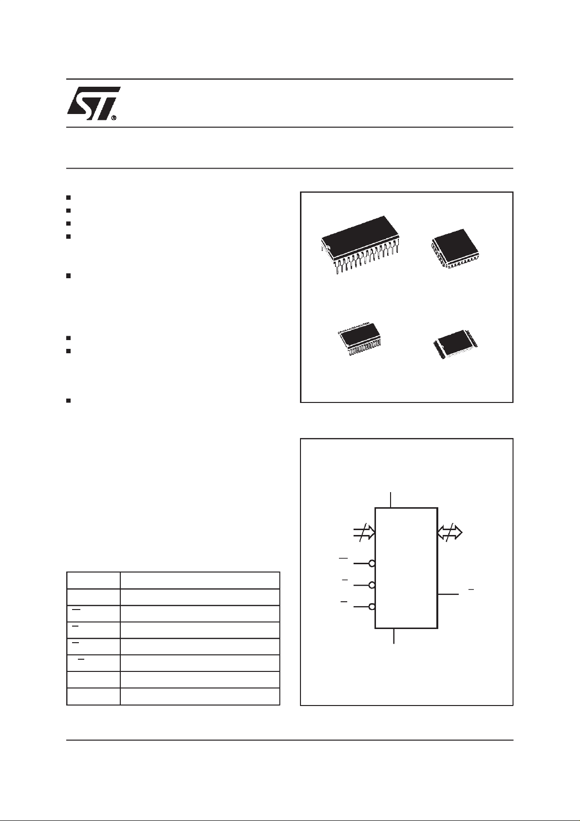
M28C64C
M28C64X
64 Kbit (8Kb x8) Parallel EEPROM
28
1
PDIP28 (P) PLCC32 (K)
28
1
SO28 (MS)
300 mils
TSOP28 (N)
8 x13.4mm
DESCRIPTION
The M28C64C is an 8 Kbit x8 low power Parallel
EEPROM fabricated with STMicroelectronics proprietary single polysilicon CMOS technology.The
device offers fast access time with low power dissipationandrequiresa 5Vpower supply.
The circuit has been designed to offer a flexible
microcontroller interface featuring both hardware
andsoftwarehandshakingmodewith Ready/Busy,
Data Polling and Toggle Bit. The M28C64C supports32 byte page write operation.
Table1. SignalNames
A0 - A12 Address Input
DQ0 - DQ7 Data Input / Output
W Write Enable
E Chip Enable
G Output Enable
RB Ready / Busy
V
CC
V
SS
Supply Voltage
Ground
Figure1. Logic Diagram
V
CC
13
A0-A12
W
E
G
M28C64C
V
SS
8
DQ0-DQ7
RB
AI00746B
February 1999 1/15
M28C64C, M28C64X
Figure2A. DIP Pin Connections
RB V
1
A12
2
A7
3
A6
4
A5
5
A4
6
A3
7
A2
A1
A0
DQ0
DQ2
SS
Warning: DU = Don’t Use.
M28C64C
8
9
10
11
12
13
14
28
27
26
25
24
23
22
21
20
19
18
17
16
15
AI00747C
Figure2C. SO Pin Connections
CC
W
DU
A8
A9
A11
G
A10
E
DQ7
DQ6
DQ5DQ1
DQ4
DQ3V
Figure2B. LCC Pin Connections
CC
DU
DU
32
W
V
A8
A9
A11
NC
G
25
A10
E
DQ7
DQ6
DQ4
DQ5
AI00748D
RB
A7
A12
A6
A5
A4
A3
A2
9
A1
A0
NC
DQ0
DQ1
Warning: NC = Not Connected, DU = Don’tUse.
1
M28C64C
17
SS
V
DQ2DUDQ3
Figure2D. TSOP Pin Connections
RB
A12
DQ0
DQ1
DQ2
V
SS
Warning: DU = Don’t Use.
A7
A6
A5
A4
A3
A2
A1
A0
1
2
3
4
5
6
7
M28C64C
8
9
10
11
12
13
14
AI00876C
V
28
27
26
25
24
23 A11
22
21
20
19
18
17
16
15
CC
W
DU
A8
A9
G
A10
E
DQ7
DQ6
DQ5
DQ4
DQ3
PIN DESCRITPION
Addresses (A0-A12).
The address inputs select
an 8-bit memory location during a read or write
operation.
G
22
A11
A9
A8
DU
W
V
CC
RB
A12
Warning: DU = Don’t Use.
Chip Enable (E).
28
M28C64C
1
A7
A6
A5
A4
A3
78
The chip enable input must be
21
15
14
AI01016D
A10
E
DQ7
DQ6
DQ5
DQ4
DQ3
V
SS
DQ2
DQ1
DQ0
A0
A1
A2
lowto enableall read/writeoperations.WhenChip
Enableis high,powerconsumptionis reduced.
OutputEnable (G).
The Output Enableinput controls the data outputbuffersand is usedto initiate
readoperations.
2/15
M28C64C, M28C64X
Table2. Absolute MaximumRatings
Symbol Parameter Value Unit
T
T
STG
V
CC
V
IO
V
V
ESD
Note:
Except for the rating ”Operating Temperature Range”, stressesabove those listed in the Table ”Absolute Maximum Ratings”may
cause permanent damage to thedevice. These are stressratings only andoperation of thedevice at these or any other conditions above
those indicated in theOperating sections of this specification is not implied. Exposure toAbsolute Maximum Rating conditions for extended
periods mayaffect device reliability.Refer also to the STMicroelectronics SURE Program and otherrelevant quality documents.
Ambient OperatingTemperature – 40 to 125 °C
A
Storage TemperatureRange – 65 to 150
Supply Voltage – 0.3 to 6.5 V
Input/Output Voltage – 0.3 to VCC+0.6 V
Input Voltage – 0.3 to 6.5 V
I
Electrostatic Discharge Voltage (Human Body model) 2000 V
C
°
Table3. OperatingModes
Mode E G W DQ0 - DQ7
Read V
Write V
Standby / Write Inhibit V
Write Inhibit X X V
Write Inhibit X V
Output Disable X V
Note:
X=V
or V
IH
IL
IL
IL
IH
V
IL
V
IH
X X Hi-Z
IL
IH
V
IH
V
IL
IH
X Data Out or Hi-Z
X Hi-Z
Data Out
Data In
Data Out or Hi-Z
DataIn/Out(DQ0-DQ7).
Datais writtentoorread
fromthe M28C64CthroughtheI/Opins.
WriteEnable(W).
TheWriteEnable inputcontrols
the writingof data to theM28C64C.
Ready/Busy (RB).
Ready/Busyis an open drain
output that can be used to detect the end of the
internalwrite cycle.
OPERATION
Inorderto prevent data corruptionandinadvertent
write operations during power-up, a Power On
Reset(POR)circuitresetsallinternalprogramming
cicuitry. Access to the memory in write mode is
allowedaftera power-upasspecifiedin Table6.
Read
The M28C64C is accessed like a static RAM.
When E and G are low with W high, the data
addressed is presented on the I/O pins. The I/O
pinsarehighimpedancewheneitherGor Eis high.
Write
Writeoperations are initiated when both W and E
arelow andG is high.TheM28C64Csupportsboth
E and W controlled write cycles. The Address is
latched by the falling edge of E or W which ever
occurslast andthe Data on the rising edge of E or
W which ever occursfirst. Once initiated the write
operationis internallytimed until completion.
Page Write
Page write allows up to 32 bytes to be consecutively latched into the memory prior to initiating a
programming cycle. All bytes must be located in a
single pageaddress, that is A5 - A12 mustbe the
samefor all bytes.The page writecan beinitiated
duringany bytewrite operation.
Following the first byte write instruction the host
may sendanotheraddressand dataup to a maximumof 100µsaftertherisingedgeof EorW which
ever occurs first (t
). If a transition of E or W is
BLC
not detected within 100µs, the internal programming cyclewill start.
3/15
M28C64C, M28C64X
Figure3. Block Diagram
RB E G W
A5-A12
(Page Address)
A0-A4
VPPGEN RESET
ADDRESS
LATCH
ADDRESS
LATCH
Y DECODE
X DECODE
ATD & CONTROL LOGIC
64K ARRAY
SENSE AND DATA LATCH
I/O BUFFERS
DQ0-DQ7
PAGE
LOAD
TIMER STATUS
TOGGLE BIT
DATA POLLING
AI00877C
MicrocontrollerControl Interface
TheM28C64Cprovidestwo writeoperation status
bitsandonestatuspin thatcanbe usedtominimize
thesystemwritecycle. Thesesignals areavailable
on the I/O port bits DQ7 or DQ6 of the memory
duringprogrammingcycleonly,or asthe RB signal
on a separate pin.
Figure4. Status Bit Assignment
DQ7 DQ6 DQ5 DQ4 DQ3 DQ2 DQ1 DQ0
DP TB PLTS Hi-Z Hi-Z Hi-Z Hi-Z Hi-Z
DP = Data Polling
TB = Toggle Bit
PLTS = Page Load TimerStatus
Data Polling bit (DQ7).
During the internal write
cycle, any attempt to read the last bytewritten will
produce on DQ7 the complementary value of the
previously latched bit. Once the write cycle is finished the true logic value appears on DQ7 in the
readcycle.
4/15
Toggle bit (DQ6).
The M28C64C offers another
way for determining when the internal write cycle
iscompleted.DuringtheinternalErase/Writecycle,
DQ6 will toggle from ”0” to ”1” and ”1” to ”0” (the
first read value is ”0”) on subsequentattemptsto
readanyaddressinthe memory.Whenthe internal
cycle is completed the toggling will stop and the
device will be accessible for a new Reador Write
operation.
Page Load Timer Status bit (DQ5). In the Page
Writemode data may be latchedby E or W up to
100µs aftertheprevious byte. Up to 32 bytes may
be input. The Data output (DQ5) indicates the
status of the internal Page Load Timer. DQ5 may
be read by asserting Output Enable Low (t
PLTS
DQ5 Low indicates the timer is running, High
indicates time-out after which the write cycle will
start and no new data may be input.
Ready/Busypin. The RB pin provides a signalat
its open drain output which is low during the
erase/write cycle, but which is released at the
completionof theprogramming cycle.
).
M28C64C, M28C64X
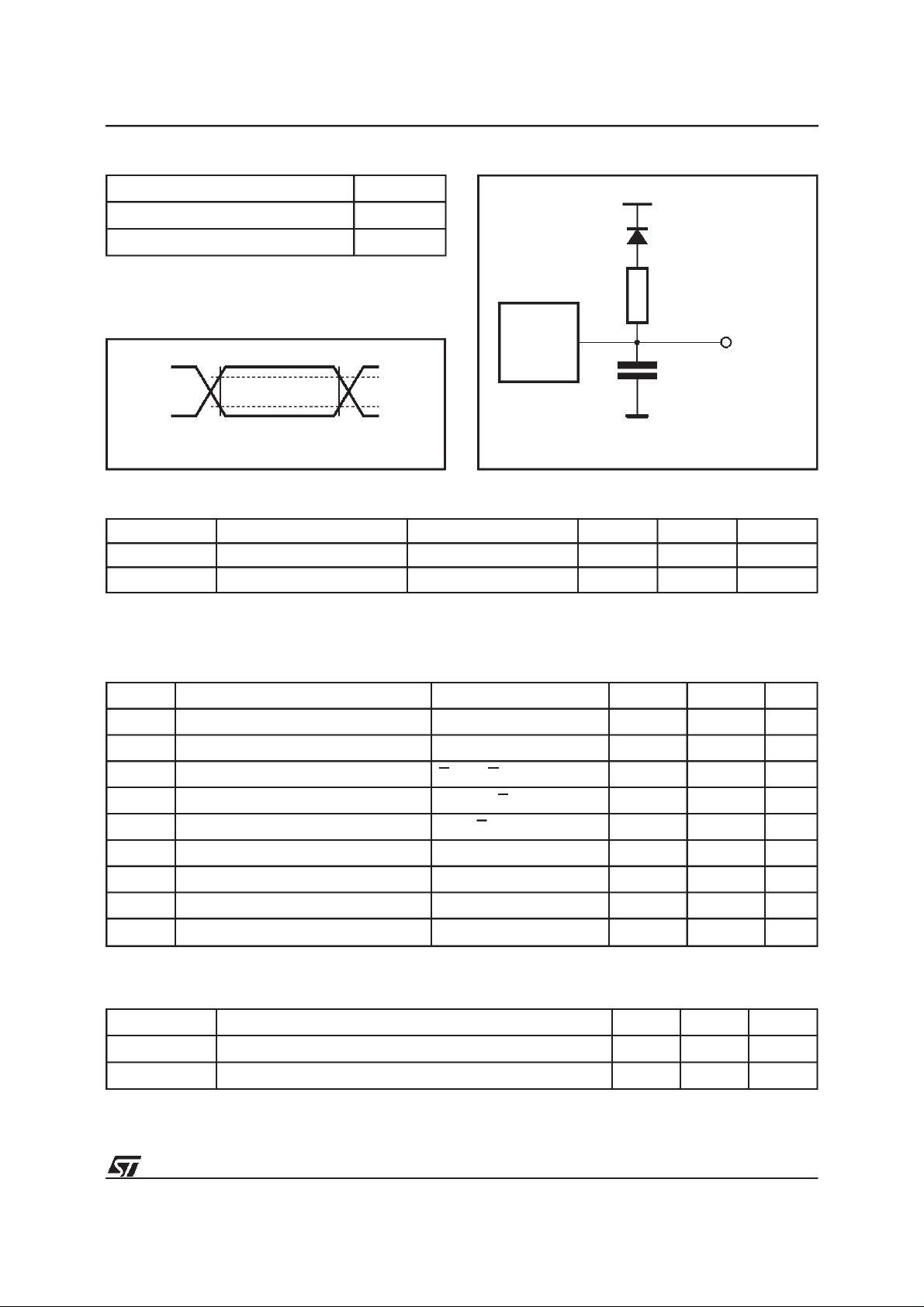
Table4. AC MeasurementConditions
Input Rise and Fall Times
≤
20ns
Figure6. AC TestingEquivalent LoadCircuit
1.3V
Input Pulse Voltages 0.4V to 2.4V
Input and Output Timing Ref. Voltages 0.8V to 2.0V
Note thatOutput Hi-Z isdefined as the point where data is no
longer driven.
Figure5. AC TestingInput Output Waveforms
2.4V
0.4V
Table5. Capacitance
(1)
(TA=25°C, f =1 MHz)
2.0V
0.8V
AI00826
DEVICE
UNDER
TEST
CLincludes JIG capacitance
1N914
3.3kΩ
CL= 30pF
Symbol Parameter Test Condition Min Max Unit
C
IN
C
OUT
Note: 1. Sampled only,not 100% tested.
Input Capacitance VIN=0V 6 pF
Output Capacitance V
=0V 12 pF
OUT
OUT
AI01129
Table6. Read ModeDC Characteristics
= 0 to70°Cor –40 to 85°C, VCC= 4.5Vto5.5V)
(T
A
Symbol Parameter TestCondition Min Max Unit
I
I
LO
I
CC
I
CC1
I
CC2
V
V
V
V
Note: 1. All I/O’s opencircuit.
Input Leakage Current 0V≤V
LI
Output Leakage Current 0V ≤ VIN≤ V
(1)
Supply Current (TTL and CMOS inputs) E = VIL,G=VIL,f=5MHz 30 mA
(1)
Supply Current (Standby) TTL E= V
(1)
Supply Current (Standby) CMOS E > VCC–0.3V 100
Input Low Voltage – 0.3 0.8 V
IL
Input High Voltage 2 VCC+0.5 V
IH
Output Low Voltage IOL= 2.1 mA 0.4 V
OL
Output High Voltage IOH= –400µA 2.4 V
OH
Table7. PowerUp Timing
(1)
=
(T
0to70°C or–40 to 85°C, V
A
V
≤
IN
CC
CC
IH
= 4.5V to 5.5V)
CC
10
10 µA
2mA
Symbol Parameter Min Max Unit
t
PUR
t
PUW
Note:
1. Sampled only,not 100% tested.
Time Delay to Read Operation 1 µs
Time Delay to Write Operation 10 ms
A
µ
A
µ
5/15

M28C64C, M28C64X
Table8. ReadModeAC Characteristics
(T
=0 to 70°C or–40 to85°C, VCC= 4.5V to 5.5V)
A
Symbol Alt Parameter Test Condition
t
t
t
t
EHQZ
AVQV
ELQV
GLQV
t
ACC
t
t
(1)
t
Address Validto
Output Valid
Chip Enable Low to
CE
Output Valid
Output Enable Low to
OE
Output Valid
Chip Enable High to
DF
Output Hi-Z
E=V
G=V
E=V
G=V
,G=V
IL
IL
IL
IL
M28C64C
-150 -200 -250
min max min max min max
IL
150 200 250 ns
150 200 250 ns
75 100 110 ns
050060065ns
Unit
(1)
t
GHQZ
t
AXQX
Note: 1. Output Hi-Z is defined as the point at which data is no longerdriven.
t
t
Output Enable High to
DF
Output Hi-Z
Address Transition to
OH
Output Transition
E=V
E=V
,G=V
IL
IL
Figure7. Read Mode AC Waveforms
A0-A12
tAVQV tAXQX
E
tGLQV tEHQZ
G
tELQV
DQ0-DQ7
VALID
050060065ns
000ns
IL
tGHQZ
DATA OUT
Hi-Z
AI00749B
Note: WriteEnable (W) = High
6/15

M28C64C, M28C64X
Table9. Write Mode AC Characteristics
(T
= 0 to 70°C or –40to85°C,V
A
Symbol Alt Parameter Test Condition Min Max Unit
=
4.5V to 5.5V)
CC
t
AVWL
t
AVEL
t
ELWL
t
GHWL
t
GHEL
t
WLEL
t
WLAX
t
ELAX
t
WLDV
t
ELDV
t
WLWH
t
ELEH
t
WHEH
t
WHGL
t
EHGL
t
t
t
CES
t
OES
t
OES
t
WES
t
t
t
t
t
WP
t
WP
t
CEH
t
OEH
t
OEH
AS
AS
AH
AH
DV
DV
Address Validto Write Enable Low E = VIL,G=V
Address Validto Chip EnableLow G = VIH,W=V
Chip Enable Low to WriteEnable Low G = V
Output EnableHigh to Write Enable
Low
Output EnableHigh to Chip Enable Low W = V
Write Enable Low to Chip EnableLow G = V
E=V
IH
IL
IL
IH
IH
IL
0ns
0ns
0ns
0ns
0ns
0ns
Write Enable Low to Address Transition 150 ns
Chip Enable Low to Address Transition 150 ns
Write Enable Low to Input Valid E = VIL,G=V
Chip Enable Low to InputValid G = VIH,W=V
IH
IL
1 µs
1 µs
Write Enable Low to Write Enable High 150 ns
Chip Enable Low to Chip EnableHigh 150 ns
Write Enable High to Chip Enable High 0 ns
Write Enable High to Output Enable
Low
10 ns
Chip Enable High to OutputEnable Low 10 ns
t
EHWH
t
WHDX
t
EHDX
t
WHWL
t
WHWH
t
WHRH
t
WHRL
t
EHRL
t
DVWH
t
DVEH
Note
: 1.With a 3.3 kΩ external pull-up resistor.
t
WEH
t
t
t
WPH
t
t
t
t
t
t
DH
DH
BLC
WC
DB
DB
DS
DS
Chip Enable High to WriteEnable High 0 ns
Write Enable High to Input Transition 0 ns
Chip Enable High to Input Transition 0 ns
Write Enable High to Write Enable Low 200 ns
Byte Load Repeat Cycle Time 0.35 50 µs
Write Cycle Time 5 ms
Write Enable High to Ready/Busy Low Note 1 220 ns
Chip Enable High to Ready/BusyLow Note 1 220 ns
Data Validbefore WriteEnable High 50 ns
Data Validbefore Chip Enable High 50 ns
7/15

M28C64C, M28C64X
Figure8. WriteMode AC Waveforms- WriteEnable Controlled
tAVWL
tELWL
VALID
tWLAX
tWLDV
DATA IN
A0-A12
E
G
tGHWL
W
DQ0-DQ7
RB
Figure9. WriteMode AC Waveforms- Chip EnableControlled
tWHEH
tWHGLtWLWH
tWHWL
tWHDXtDVWH
tWHRL
AI00750
8/15
A0-A12
E
G
W
DQ0-DQ7
RB
tAVEL
tGHEL
tWLEL
VALID
tELAX
tELDV
tELEH
tEHGL
tEHWH
DATA IN
tEHDXtDVEH
tEHRL
AI00751

Figure10. PageWriteMode AC Waveforms - Write EnableControlled
M28C64C, M28C64X
A0-A12
E
G
W
DQ0-DQ7
DQ5
RB
tWLWH
Addr 0
tWHWL
Byte 0 Byte 1 Byte 2 Byte n
Addr 1 Addr 2 Addr n
tWHWH
tWHRL
tPLTS
tWHRH
tWHWH
Byte n
AI00752C
Figure11.Data Polling WaveformSequence
A0-A12
E
G
W
DQ7
Address of thelast byte of the Page Write instruction
DQ7 DQ7DQ7 DQ7DQ7
READYLAST WRITE INTERNAL WRITE SEQUENCE
AI00753C
9/15

M28C64C, M28C64X
Figure12. Toggle Bit Waveform Sequence
A0-A12
E
G
W
DQ6
Note: 1. First Togglebit is forced to ’0’
ORDERING INFORMATION SCHEME
Example: M28C64C -150 K 1
Version
C RB available
X RB not bonded
(pin NC)
-150 150 ns
-200 200 ns
-250 250 ns
(1)
TOGGLE
INTERNAL WRITE SEQUENCE
Speed
MS SO28 300mils
Package
P PDIP28
K PLCC32
N TSOP28
8 x 13.4mm
READYLAST WRITE
AI00754D
TemperatureRange
1 0 to 70 °C
6 –40 to 85°C
Fora listof availableoptions(Speed,Package,etc... ) orforfurtherinformationonanyaspectofthisdevice,
pleasecontactthe STMicroelectronics Sales Officenearest to you.
10/15

PDIP28 - 28 pin PlasticDIP, 600 mils width
M28C64C, M28C64X
Symb
Typ Min Max Typ Min Max
A 5.08 0.200
A1 0.38 0.015
A2 3.56 4.06 0.140 0.160
B 0.38 0.51 0.015 0.020
B1 1.52 0.060
C 0.20 0.30 0.008 0.012
D 36.83 37.34 1.450 1.470
D2 33.02 1.300
E 15.24 0.600
E1 13.59 13.84 0.535 0.545
e1 2.54 0.100
eA 14.99 0.590
eB 15.24 17.78 0.600 0.700
L 3.18 3.43 0.125 0.135
S 1.78 2.08 0.070 0.082
α 0° 10° 0° 10°
N28 28
mm inches
Drawing is not to scale.
B1 B e1
D2
D
S
N
1
A2A1A
E1 E
L
α
C
eA
eB
PDIP
11/15

M28C64C, M28C64X
PLCC32 - 32 lead PlasticLeadedChip Carrier,rectangular
Symb
Typ Min Max Typ Min Max
A 2.54 3.56 0.100 0.140
A1 1.52 2.41 0.060 0.095
A2 – 0.38 – 0.015
B 0.33 0.53 0.013 0.021
B1 0.66 0.81 0.026 0.032
D 12.32 12.57 0.485 0.495
D1 11.35 11.56 0.447 0.455
D2 9.91 10.92 0.390 0.430
E 14.86 15.11 0.585 0.595
E1 13.89 14.10 0.547 0.555
E2 12.45 13.46 0.490 0.530
e 1.27 – – 0.050 – –
F 0.00 0.25 0.000 0.010
R 0.89 – – 0.035 – –
N32 32
Nd 7 7
Ne 9 9
CP 0.10 0.004
mm inches
D
D1
1N
Ne E1 E
Nd
PLCC
Drawing is notto scale.
12/15
R
F
0.51 (.020)
1.14 (.045)
D2/E2
A1
A2
B1
e
B
A
CP

M28C64C, M28C64X
SO28 - 28 lead Plastic Small Outline, 300 mils body width
Symb
Typ Min Max Typ Min Max
A 2.46 2.64 0.097 0.104
A1 0.13 0.29 0.005 0.011
A2 2.29 2.39 0.090 0.094
B 0.35 0.48 0.014 0.019
C 0.23 0.32 0.009 0.013
D 17.81 18.06 0.701 0.711
E 7.42 7.59 0.292 0.299
e 1.27 – – 0.050 – –
H 10.16 10.41 0.400 0.410
L 0.61 1.02 0.024 0.040
α 0° 8° 0° 8°
N28 28
CP 0.10 0.004
mm inches
Drawing is not to scale.
A2
A
C
B
e
CP
D
N
E
H
1
LA1 α
SO-b
13/15

M28C64C, M28C64X
TSOP28- 28 lead Plastic Thin Small Outline,8 x 13.4mm
Symb
Typ Min Max Typ Min Max
A 1.25 0.049
A1 0.20 0.008
A2 0.95 1.15 0.037 0.045
B 0.17 0.27 0.007 0.011
C 0.10 0.21 0.004 0.008
D 13.20 13.60 0.520 0.535
D1 11.70 11.90 0.461 0.469
E 7.90 8.10 0.311 0.319
e 0.55 – – 0.022 – –
L 0.50 0.70 0.020 0.028
α
N28 28
CP 0.10 0.004
mm inches
0
°
5
°
0
°
5
°
Drawing is not to scale.
28
1
22
21
E
78
D1
D
DIE
TSOP-c
A2
e
B
A
CP
C
LA1 α
14/15

M28C64C, M28C64X
Information furnished is believed to be accurate and reliable. However, STMicroelectronics assumesno responsibility for the consequences
ofuse of such informationnor for any infringementof patents orother rights ofthirdparties whichmay resultfrom itsuse. No licenseis granted
by implicationor otherwise under any patentor patent rights of STMicroelectronics.Specificationsmentioned in thispublication are subjectto
change without notice. This publication supersedes and replaces all information previously supplied. STMicroelectronics products are not
authorized for use as criticalcomponents in lifesupport devices or systems withoutexpress written approvalof STMicroelectronics.
The ST logo is a registeredtrademark ofSTMicroelectronics
1999 STMicroelectronics - AllRights Reserved
All other names are the property of theirrespective owners
Australia - Brazil- Canada - China - France - Germany - Italy - Japan - Korea - Malaysia - Malta- Mexico - Morocco -The Netherlands-
Singapore - Spain - Sweden - Switzerland- Taiwan - Thailand - UnitedKingdom -U.S.A.
STMicroelectronics GROUP OF COMPANIES
http://www.st.com
15/15
 Loading...