

SGS Thomson Microelectronics M27V320 Datasheet
32 Mbit (4Mb x8 or 2Mb x16) OTP EPROM
■ 3.3V ± 10% SUPPLY VOLTAGE in READ
OPERATION
■ ACCESS TIME: 100ns
■ BYTE-WIDE or WORD-WIDE
CONFIGURABLE
■ 32 Mbit MASK ROM REPLACEMENT
■ LOW POWER CONSUMPTION
– Active Current 30mA at 5MHz
– Standby Current 60µA
■ PROGRAMMI NG VOLT AGE: 12V ± 0.2 5 V
■ PROGRAMMING TIME: 50µs/word
■ ELECTRONIC SIGNATURE:
– Manufacturer Code 20h
– Device Code: 32h
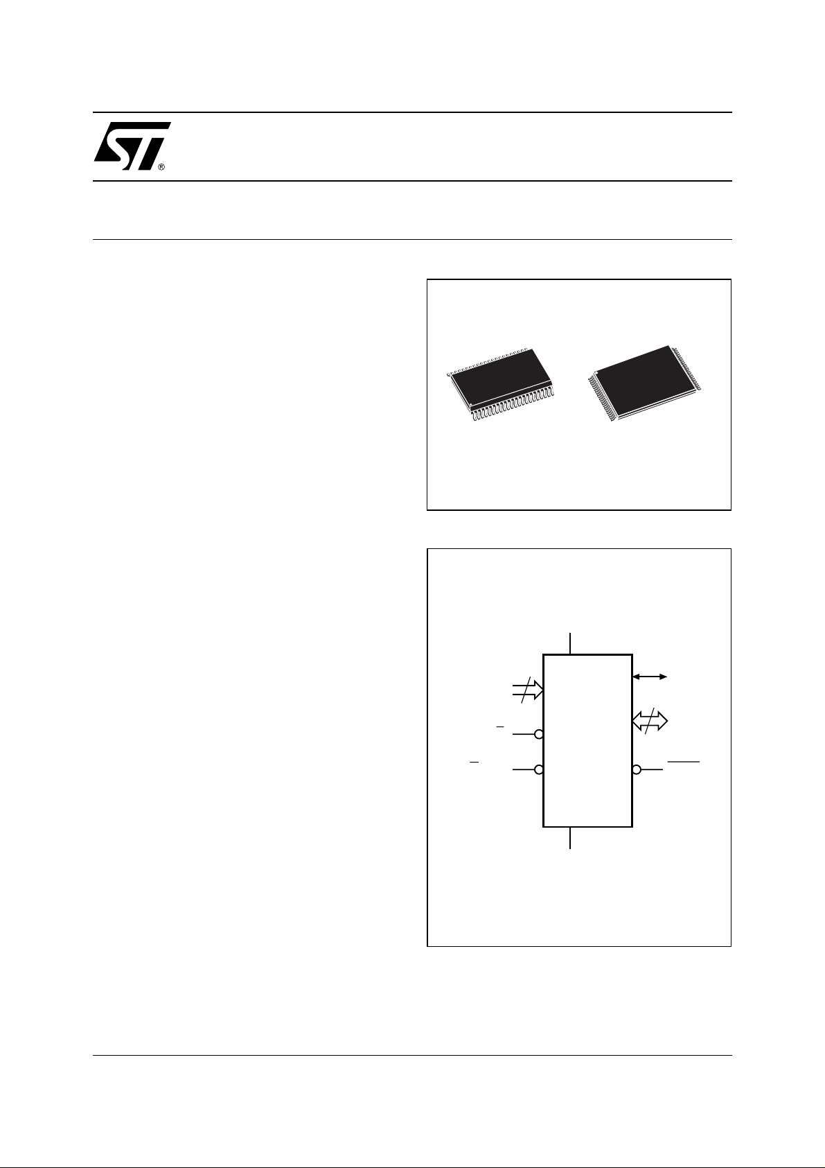
M27V320
SO44 (M) TSOP48 (N)
12 x 20 mm
Figure 1. Logic Diagram
DESCRIPTION
The M27V320 is a low voltage 32 Mbit EPROM offered in the OTP range (one time programmable).
It is ideally suited for microprocessor systems requiring large data or program st orage. It is organised as either 4 MWords of 8 bit or 2 MWords of 16
bit. The pin-out is compatible with the 32 Mbit
Mask ROM.
The M27V320 is offered in SO44 and TSOP48
(12 x 20 mm) packages.
A0-A20
GV
PP
V
CC
21
E
M27V320
V
SS
Q15A–1
15
Q0-Q14
BYTE
AI05852
1/15August 2002
M27V320
Figure 2. SO Connections
NC A20
A17 A8
A7
A6
A5
A4
A3
A2
A1
A0
V
SS
GV
PP
Q0
Q8
Q9
Q10
Q3
Q11
1
2
3
4
5
6
7
8
9
10
11
M27V320
12
E
13
14
15
16
17Q1
18
19
20
21
44
43
42
41
40
39
38
37
36
35
34
33
32
31
30
29
28
27
26
25
24
2322
AI05853
A19A18
A9
A10
A11
A12
A13
A14
A15
A16
BYTE
V
SS
Q15A–1
Q7
Q14
Q6
Q13
Q5Q2
Q12
Q4
V
CC
Figure 3. TSOP Connections
BYTE
A16
A15
A14
A13
A12
A10
A19
V
SS
A20
A18
A17
1
A9
A8
12
13
A7
A6
A5
A4
A2
A1
A0
24 25
E
M27V320
48
37
36
AI05854
V
SS
V
SS
Q15A–1
Q7
Q14
Q6
Q13A11
Q5
Q12
Q4
V
CC
V
CC
V
SS
Q11
Q3
Q10
Q2
Q9
Q1
Q8A3
Q0
GV
PP
V
SS
V
SS
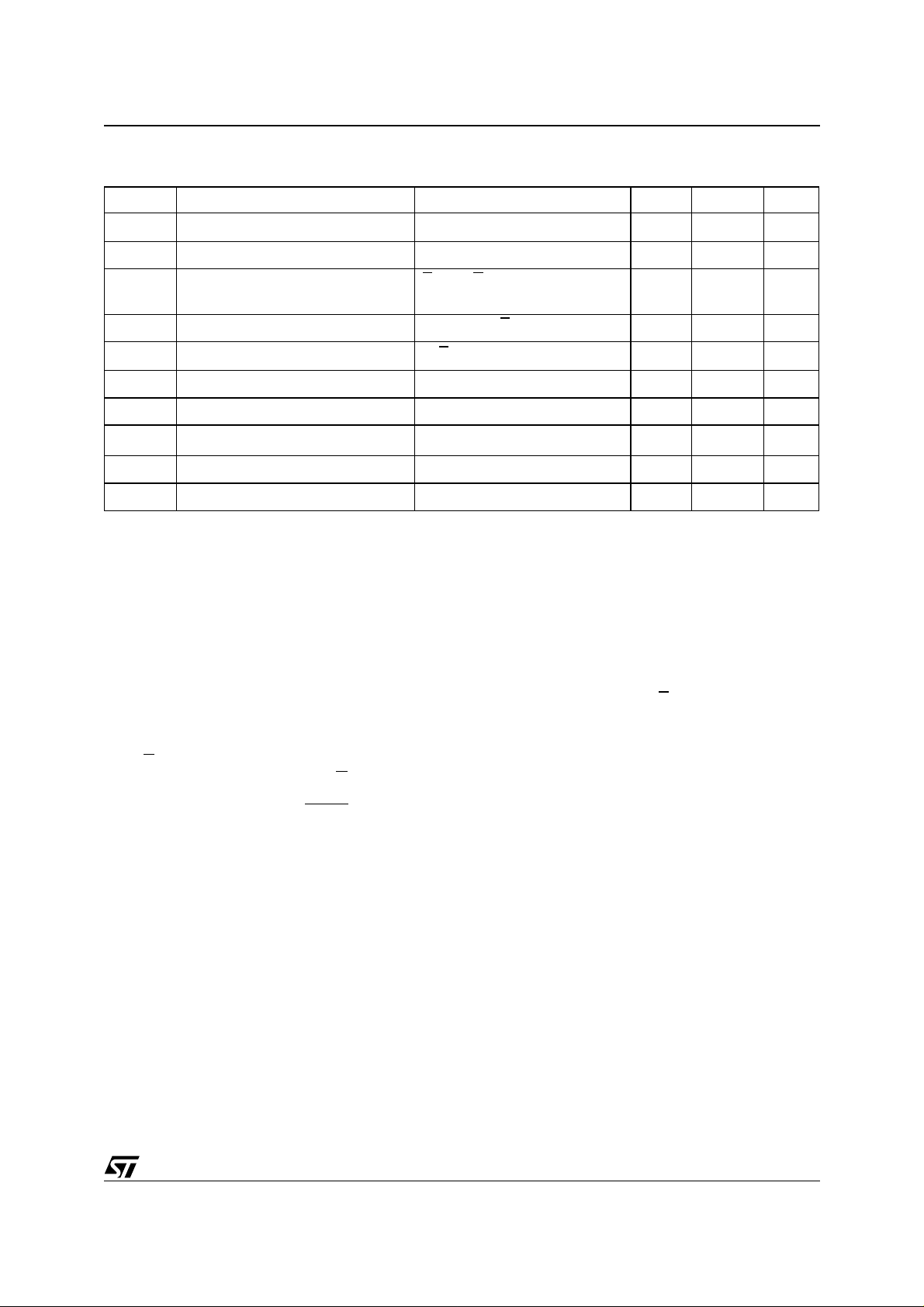
Table 1. Signal Names
A0-A20 Address Inputs
Q0-Q7 Data Outputs
Q8-Q14 Data Outputs
Q15A–1 Data Output / Address Input
E
G
V
PP
BYTE Byte-Wide Select
V
CC
V
SS
NC Not Connected Internally
2/15
Chip Enable
Output Enable / Program Supply
Supply Voltage
Ground
DEVICE OPERATION
The operating modes of the M27V320 are listed in
the Operating Modes Table. A single power supply
is required in the read mode. All inputs are TTL
compatib le exc ept for V
and 12V on A9 for the
PP
Electronic Signature.
Read Mode
The M27V32 0 has two organisations, Word-wide
and Byte-wide. The organisation is selected by the
signal level on the BYTE
pin. When BYTE is at V
the Word-wide organisation is selected and the
Q15A–1 pin is used for Q15 Data Output. When
the BY T E
pin is at VIL the Byte-wide organisat ion
is selected and the Q15A–1 pin is used for the Address Input A–1. When the memory is logically regarded as 16 bit wide, but read in the Byte-wide
organisation, then with A–1 at V
the lower 8 bits
IL
of the 16 bit data are selected and with A–1 at V
the upper 8 bits of the 16 bit data are selected.
IH
IH
M27V320
Table 2. Absolute Maximum Ratings
(1)
Symbol Parameter Value Unit
T
A Ambient Operating Temperature
T
BIAS
T
STG
(2)
V
IO
V
CC
(2)
V
A9
V
PP
Note: 1. Except for the ratin g "Operating Temperat ure Range", stresse s above th ose listed i n t he Table "Absolute M aximum Rat i ngs" may
cause permanent damage to the device. These are stress ratings only and operation of the device at these or any other conditions
above those indi cated in t he Operating secti ons of t hi s specifi cation i s not impl i ed. Exposure to Absolute Maximum Rating conditions for extended per iods may aff ect device reliabilit y. Refer also to the STMicroe lectronics SURE Program an d other relevan t quality docum en ts .
2. Minimum DC vo ltage on Inpu t or Out put is – 0.5V w ith poss ible un dershoot to –2. 0V fo r a peri od les s than 20ns. Ma ximum DC
voltage on Output is V
3. Depends on range.
Temperature Under Bias –50 to 125 °C
Storage Temperature –65 to 150 °C
Input or Output Voltage (except A9) –2 to 7 V
Supply Voltage –2 to 7 V
A9 Voltage –2 to 13.5 V
Program Supply Voltage –2 to 14 V
+0.5V with possible overshoot to VCC +2V for a period l ess than 20ns.
CC
(3)
–40 to 125 °C
Table 3. Operating Modes
Mode E
Read Word-wide
Read Byte-wide Upper
Read Byte-wide Lower
Output Disable
Program
Program Inhibit
Standby
Electronic Signature
Note: X = VIH or VIL, VID = 12V ± 0.5V.
V
V
V
V
V
Pulse V
IL
V
V
V
GV
PP
IL
IL
IL
IL
IH
IH
IL
V
IL
V
IL
V
IL
V
IH
PP
V
PP
X X X Hi-Z Hi-Z Hi-Z
V
IL
BYTE A9 Q15A–1 Q14-Q8 Q7-Q0
V
IH
V
IL
V
IL
X Data Out Data Out Data Out
X
X
V
IH
V
IL
Hi-Z Data Out
Hi-Z Data Out
X X Hi-Z Hi-Z Hi-Z
V
IH
V
IH
V
IH
X Data In Data In Data In
X Hi-Z Hi-Z Hi-Z
V
ID
Code Codes Codes
Table 4. Electronic Signature
Identifier A0 Q7 Q6 Q5 Q4 Q3 Q2 Q1 Q0 Hex Data
Manufacturer’s Code
Device Code
Note: Output s Q15-Q8 are s et to '0' .
V
V
IL
IH
00100000 20h
00110010 32h
3/15
M27V320
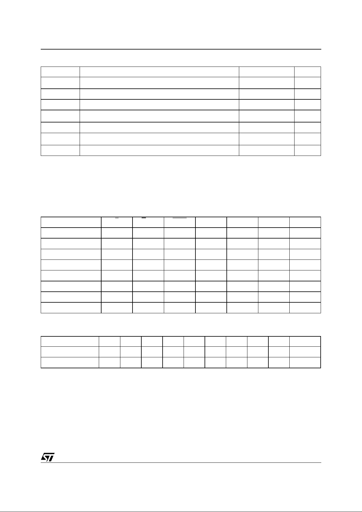
Table 5. AC Measurement Conditions
High Speed Standard
Input Rise and Fall Times ≤ 10ns ≤ 20ns
Input Pulse Voltages 0 to 3V 0.4V to 2.4V
Input and Output Timing Ref. Voltages 1.5V 0.8V and 2V
Figure 4. AC Testing Input Output Waveform
High Speed
3V
1.5V
0V
Standard
2.4V
0.4V
Table 6. Capacitance
Symbol Parameter Test Condition Min Max Unit
C
IN
C
OUT
Note: 1. Sampled only, not 100% tested.
(1)
(TA = 25 °C, f = 1 MHz)
Input Capacitance
Output Capacitance
2.0V
0.8V
AI01822
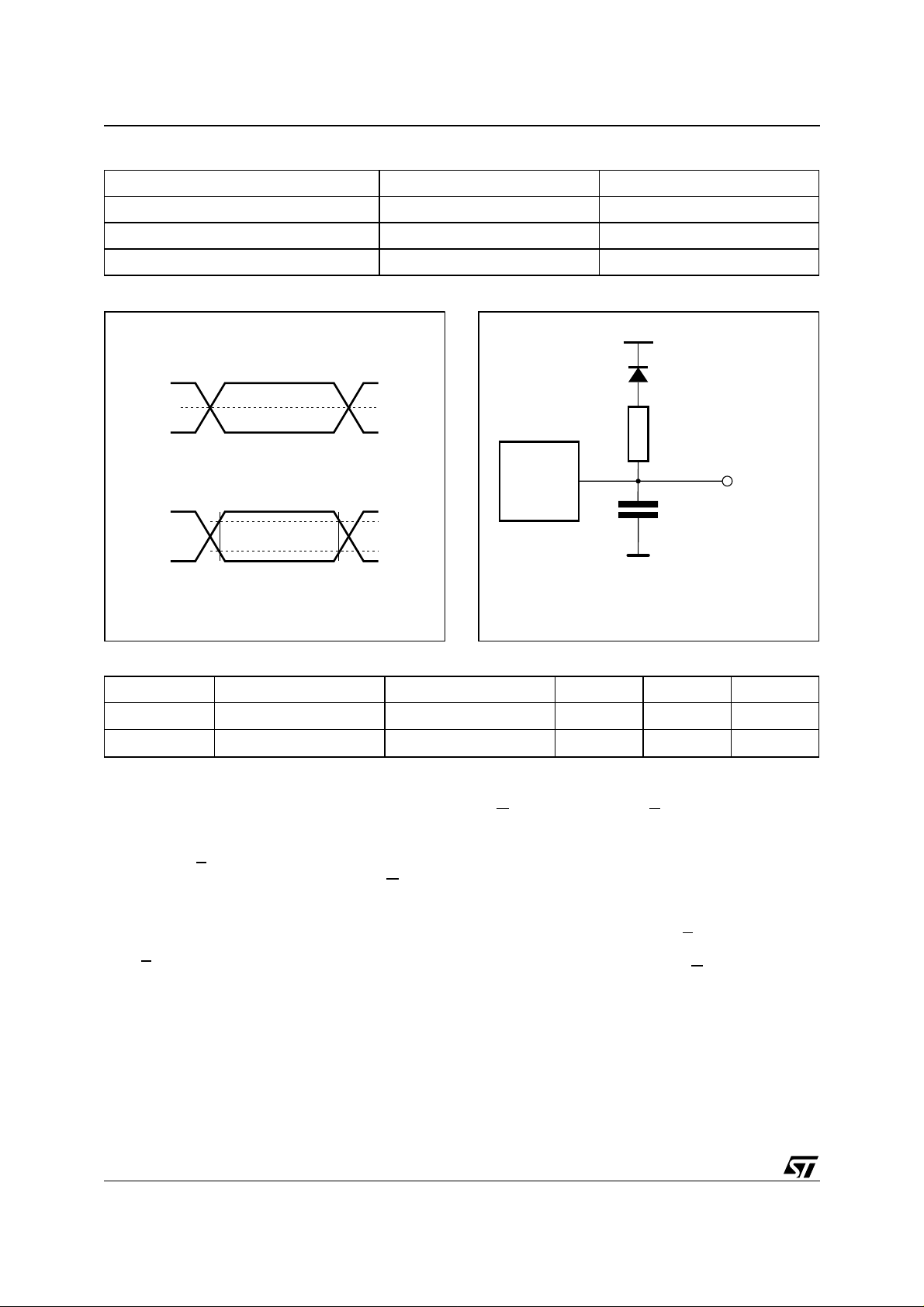
Figure 5. AC Testing Load Circuit
1.3V
DEVICE
UNDER
TEST
CL = 30pF for High Speed
CL = 100pF for Standard
CL includes JIG capacitance
V
= 0V
IN
V
= 0V
OUT
1N914
3.3kΩ
CL
10 pF
12 pF
OUT
AI01823B
The M27V320 ha s two control functions, both of
which must be logically ac tive in order to obtain
data at the outputs. In addition the Word-wide or
Byte-wide organisation must be selected.
Chip Enable (E
used for device selection. Output Enable (G
) is the power control and should be
VPP) is
the output control and should be used to gate data
to the output pins independent of device selection.
Assuming that the addresses are s table, the address access time (t
from E
to output (t
4/15
ELQV
) is equal to the delay
AVQV
). Data is available at the
output after a delay of t
of G
VPP, assuming that E has been low and t he
addresses have been stable for at least t
t
.
GLQV
from the falling e dge
GLQV
AVQV
Standby Mode
The M27V320 has standby mode which reduces
the supply current from 50mA to 100µA. The
M27V320 is placed in the standby mode by applying a CMOS high signal to the E
input. When in the
standby mode, the outputs are in a high impedance state, independent of the G
VPP input.
-
M27V320
Table 7. Read Mode DC Characteristics
(1)
(TA = 0 to 70°C or –40 to 85°C; VCC = 3.3V ± 10%; VPP = VCC)
Symbol Parameter Test Condition Min Max Unit
I
I
I
CC
I
CC
I
CC
I
V
VIH
V
V
Note: 1. VCC must be ap pl i e d simultaneously with or before VPP and removed simultane ously or aft er VPP.
Two Line Outp ut C ontrol
Because EPROMs are usually used in larger
memory arrays, this product features a 2 line control function which accommodates the use of multiple memory connection. The two line control
function allows:
a. the lowest possible memory power dissipation,
b. comple te assuranc e that output bus contention
will not occur.
For the most efficient use of these two control
lines, E
ry device selecting function, while G
made a common connectio n to all devices in the
array and connected to the READ
system control bus. This ensures that all deselected memory devices are in their low power standby
mode and that the output pins are only active
when data is required from a particular memory
device.
Input Leakage Current
LI
Output Leakage Current
LO
Supply Current
1
Supply Current (Standby) TTL
2
Supply Current (Standby) CMOS E
Program Current
PP
Input Low Voltage –0.6
IL
(2)
Input High Voltage
Output Low Voltage
OL
Output High Voltage TTL
OH
2. Maximu m DC voltage on Ou tput is V
CC
+0.5 V .
E
0V ≤ V
0V ≤ V
= VIL, GVPP = VIL, I
f = 5MHz, V
> VCC – 0.2V, VCC ≤ 3.6V 60 µA
I
IN
OUT
E = V
V
= V
PP
I
= 2.1mA
OL
= –400µA
OH
≤ V
≤ V
≤ 3.6V
CC
IH
CC
CC
CC
OUT
System Considerations
The power switching characteristics of Advanced
CMOS EPROMs require careful decoupling of the
supplies to the devices. The supply current I
has three segments of importance to the system
designer: the standby current, the active current
and the transient peaks that are produced by the
falling and rising edges of E
The magnitude of the transient current peaks is
dependent on the capacitive and inductive loading
should be decoded and used as the prima-
VPP should be
line from the
of the device outputs. The associated transient
voltage peaks can be suppressed by complying
with the two line output control and by properly selected decoupling capacitors . It is recommended
that a 0.1µF ceramic capacitor is used o n every
device between V
high frequency type of low inherent inductance
and should be placed as close as possible to the
device. In addition, a 4.7µF electro lytic capacitor
should be used between V
= 0mA,
CC
±1 µA
±10 µA
30 mA
1mA
10 µA
0.2V
CC
0.7V
CCVCC
2.4 V
+ 0.5
0.4 V
.
and VSS. This sho uld be a
and VSS for every
CC
eight devices. This capacitor should be mounted
near the power supply connect ion point. The purpose of this capacitor is to overcome the voltage
drop caused by the inductive ef fects of PC B traces.
V
V
CC
5/15
 Loading...