

SGS Thomson Microelectronics M27C512-90XN6TR, M27C512-90XN6, M27C512-90XN3TR, M27C512-90XN3, M27C512-90XN1TR Datasheet
...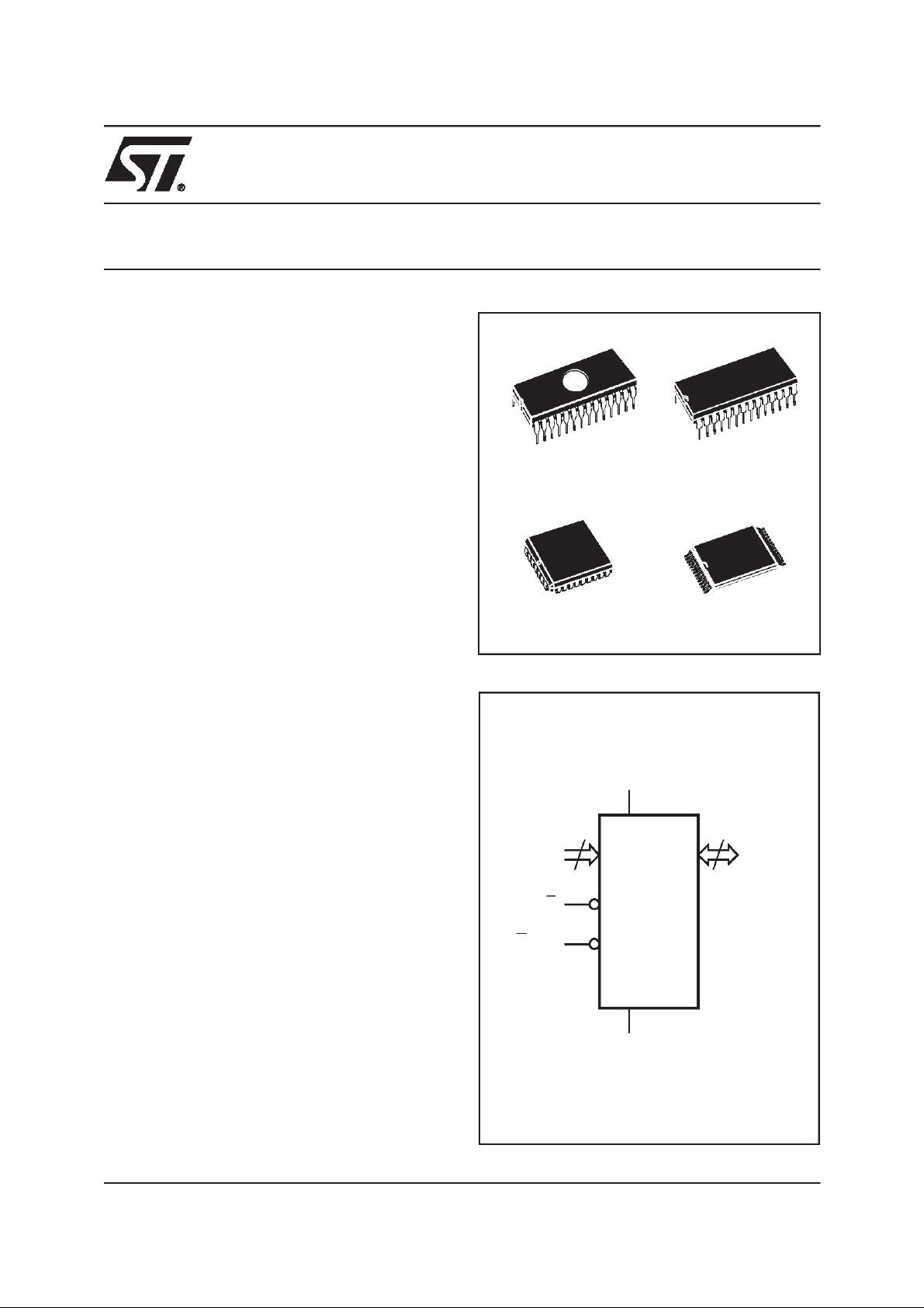
512 Kbit (64Kb x8) UV EPROM and OTP EPROM
■ 5V ± 10% SUPPLY VOLTAGE in READ
OPERATION
■ ACCESS TIME: 45ns
■ LOW POWER “CMOS” CONSUMPTION:
– Active Current 30mA
– Standby Current 100µA
■ PROGRAMMING VOLTAGE: 12.75V ± 0.25V
■ PROGRAMMING TIMES of AROUND 6sec.
■ ELECTRONIC SIGNATURE
– Manufacturer Code: 20h
– Device Code: 3Dh
DESCRIPTION
The M27C512 is a 512 Kbit EPROM offered in the
two ranges UV (ultra violet erase) and OTP (one
time programmable). It is ideally suited for applications where fast turn-around and pattern experimentation are important requirements and is
organized as 65,536 by 8 bits.
The FDIP28W (window ceramic frit-seal package)
has transparent lid which allows the user to expose the chipto ultraviolet light to erase thebitpattern. A new pattern can then be written to the
device by following the programming procedure.
For applications wherethe content is programmed
only one time and erasure is not required, the
M27C512 is offered in PDIP28, PLCC32 and
TSOP28 (8 x 13.4 mm) packages.
28
1
FDIP28W (F) PDIP28 (B)
PLCC32 (C) TSOP28 (N)
28
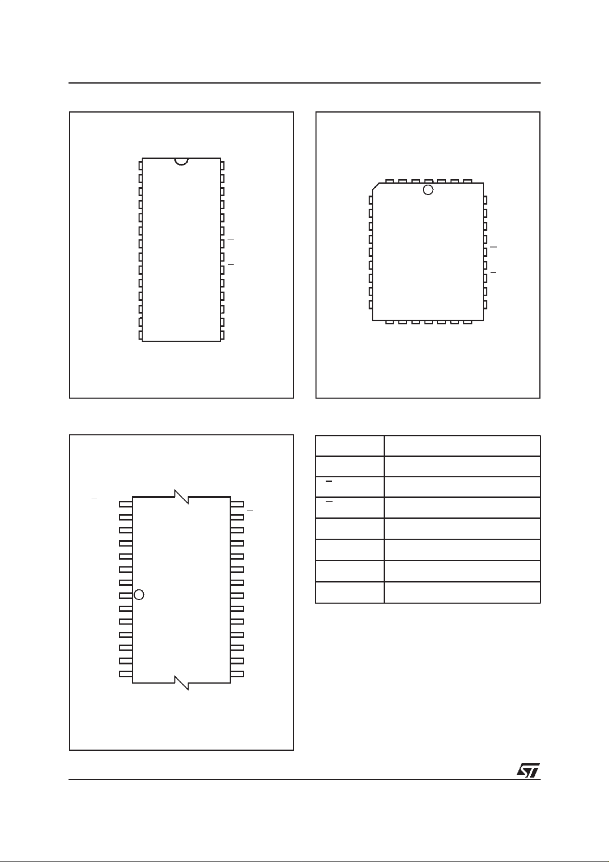
Figure 1. Logic Diagram
V
CC
16
A0-A15
M27C512
1
8 x 13.4 mm
8
Q0-Q7
GV
PP
E
M27C512
V
SS
AI00761B
1/18April 2001
M27C512
Figure 2A. DIP Connections
A15 V
1
A12
2
A7
3
A6
4
A5
5
A4
6
A3
7
8
9
10
11
12
13
14
M27C512
A2
A1
A0
Q0
Q2
SS
28
27
26
25
24
23
22
21
20
19
18
17
16
15
AI00762
CC
A14
A13
A8
A9
A11
GV
A10
E
Q7
Q6
Q5Q1
Q4
Q3V
PP
Figure 2B. LCC Connections
A15
A6
A5
A4
A3
A2
A1
A0
NC
Q0
A7
9
Q1
DU
A12
1
M27C512
17
Q2
SS
DU
V
V
32
Q3
CC
A14
Q4
A13
25
Q5
A8
A9
A11
NC
GV
A10
E
Q7
Q6
AI00763
PP
Figure 2C. TSOP Connections
GV
A11
A13
A14
V
A15
A12
PP
A9
A8
CC
A7
A6
A5
A4
A3
22
28
M27C512
1
78
AI00764B
21
15
14
A10
E
Q7
Q6
Q5
Q4
Q3
V
SS
Q2
Q1
Q0
A0
A1
A2
Table 1. Signal Names
A0-A15 Address Inputs
Q0-Q7 Data Outputs
E Chip Enable
GV
V
V
NC
DU
PP
CC
SS
Output Enable / Program Supply
Supply Voltage
Ground
Not Connected Internally
Don’t Use
2/18
M27C512
Table 2. Absolute Maximum Ratings
(1)
Symbol Parameter Value Unit
T
A
T
BIAS
T
STG
(2)
V
IO
V
CC
(2)
V
A9
V
PP
Note: 1. Except for the rating ”Operating Temperature Range”, stresses above those listed in the Table ”Absolute Maximum Ratings” may
cause permanent damage to the device. These are stress ratings only and operation of the device at these or any other conditions
above those indicated in the Operating sections of this specification is not implied. Exposure to Absolute Maximum Rating conditions for extended periods may affect device reliability. Refer also to the STMicroelectronics SURE Program and otherrelevant quality documents.
2. Minimum DC voltage on Input or Output is –0.5V with possible undershoot to –2.0V for a period less than 20ns. Maximum DC
voltage on Output is V
3. Depends on range.
Ambient Operating Temperature
Temperature Under Bias –50 to 125 °C
Storage Temperature –65 to 150 °C
Input or Output Voltage (except A9) –2 to 7 V
Supply Voltage –2 to 7 V
A9 Voltage –2 to 13.5 V
Program Supply Voltage –2 to 14 V
+0.5V with possible overshoot to VCC+2V for a period less than 20ns.
CC
(3)
–40 to 125 °C
Table 3. Operating Modes
Mode E
Read
Output Disable V
Program
V
Program Inhibit V
Standby
Electronic Signature
Note: X = VIHor VIL,VID= 12V ± 0.5V.
V
IL
IL
Pulse V
IL
IH
V
IH
V
IL
GV
V
PP
V
IL
V
IH
PP
PP
A9 Q7-Q0
X Data Out
X Hi-Z
XDataIn
X Hi-Z
X X Hi-Z
V
IL
V
ID
Codes
Table 4. Electronic Signature
Identifier A0 Q7 Q6 Q5 Q4 Q3 Q2 Q1 Q0 Hex Data
Manufacturer’s Code
Device Code
V
IL
V
IH
00100000 20h
00111101 3Dh
3/18
M27C512
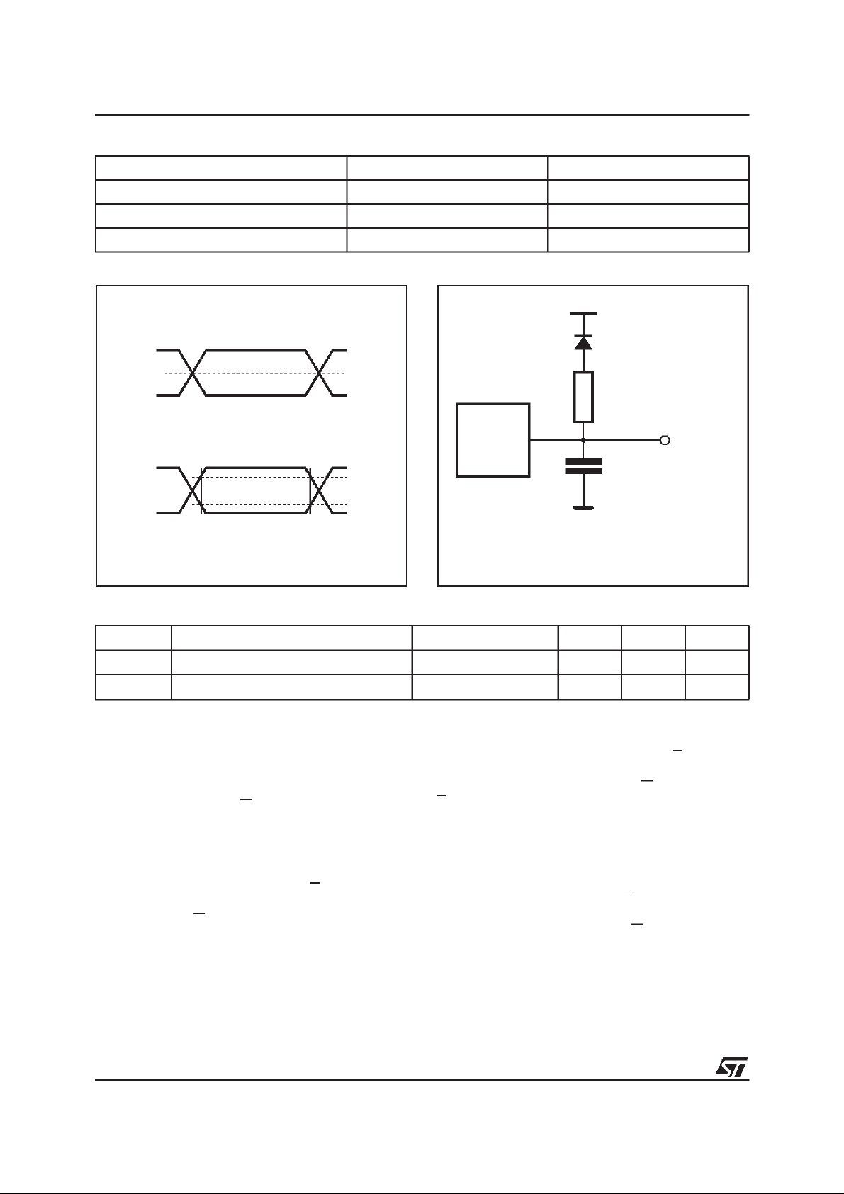
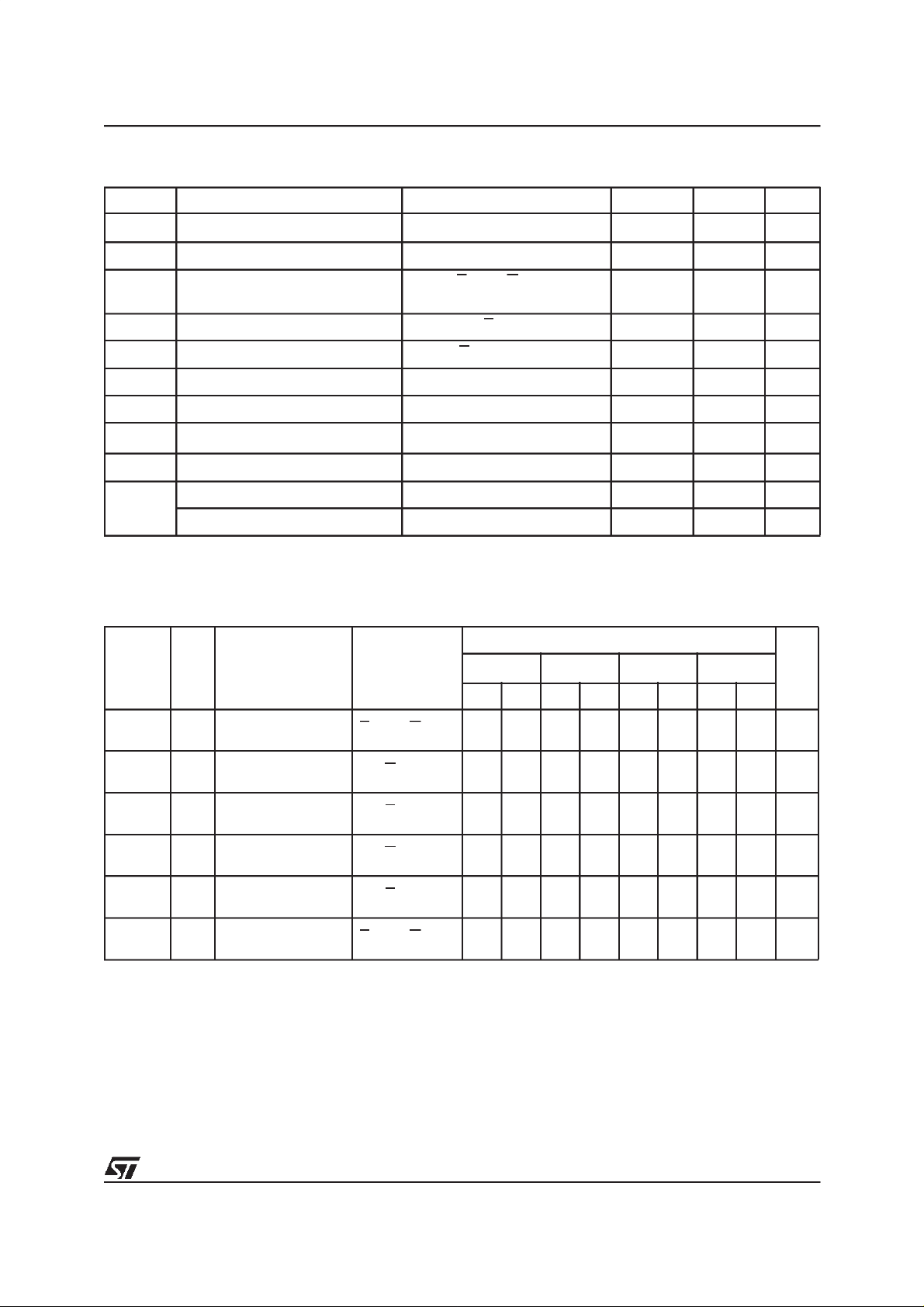
Table 5. AC Measurement Conditions
High Speed Standard
Input Rise and Fall Times ≤ 10ns ≤ 20ns
Input Pulse Voltages 0 to 3V 0.4V to 2.4V
Input and Output Timing Ref. Voltages 1.5V 0.8V and 2V
Figure 3. Testing Input Output Waveform
High Speed
3V
1.5V
0V
Standard
2.4V
0.4V
Table 6. Capacitance
Symbol Parameter Test Condition Min Max Unit
C
IN
C
OUT
Note: 1. Sampled only, not 100% tested.
Input Capacitance
Output Capacitance
(1)
(TA=25°C, f = 1 MHz)
2.0V
0.8V
AI01822
Figure 4. AC Testing Load Circuit
1.3V
1N914
3.3kΩ
DEVICE
UNDER
TEST
C
L
CL= 30pF for High Speed
CL= 100pF for Standard
CLincludes JIG capacitance
V
V
IN
OUT
=0V
=0V
6pF
12 pF
OUT
AI01823B
DEVICE OPERATION
The modes of operations of the M27C512 are listed in the Operating Modes table. A single power
supply is required in the read mode. All inputs are
TTL levels except for GVPPand 12V on A9 for
Electronic Signature.
Read Mode
The M27C512 has two control functions, both of
which must be logically active in order to obtain
data at the outputs. Chip Enable (E) is the power
control and should be used for device selection.
Output Enable(G) is the output control and should
be used to gate data to the output pins, independent of device selection. Assuming that the ad-
4/18
dresses are stable, the address access time
(t
) is equal to the delay from E to output
AVQV
(t
). Data is availableat the output after a delay
ELQV
of t
from the falling edge of G, assuming that
GLQV
E has been low and the addresses have been stable for at least t
AVQV-tGLQV
.
Standby Mode
The M27C512 has a standby mode which reduces
the active current from 30mA to 100µA The
M27C512 is placed in the standby mode by applying aCMOS highsignal to the Einput. When in the
standby mode, the outputs are in a high impedance state, independent of the GVPPinput.
M27C512
Table 7. Read Mode DC Characteristics
(1)
(TA= 0 to 70 °C, –40 to 85 °C or –40 to 125 °C; VCC=5V±5% or 5V ± 10%; VPP=VCC)
Symbol Parameter Test Condition Min Max Unit
I
I
I
CC
I
CC1
I
CC2
I
V
V
IH
V
V
Note: 1. VCCmust be applied simultaneously with or before VPPand removed simultaneously or after VPP.
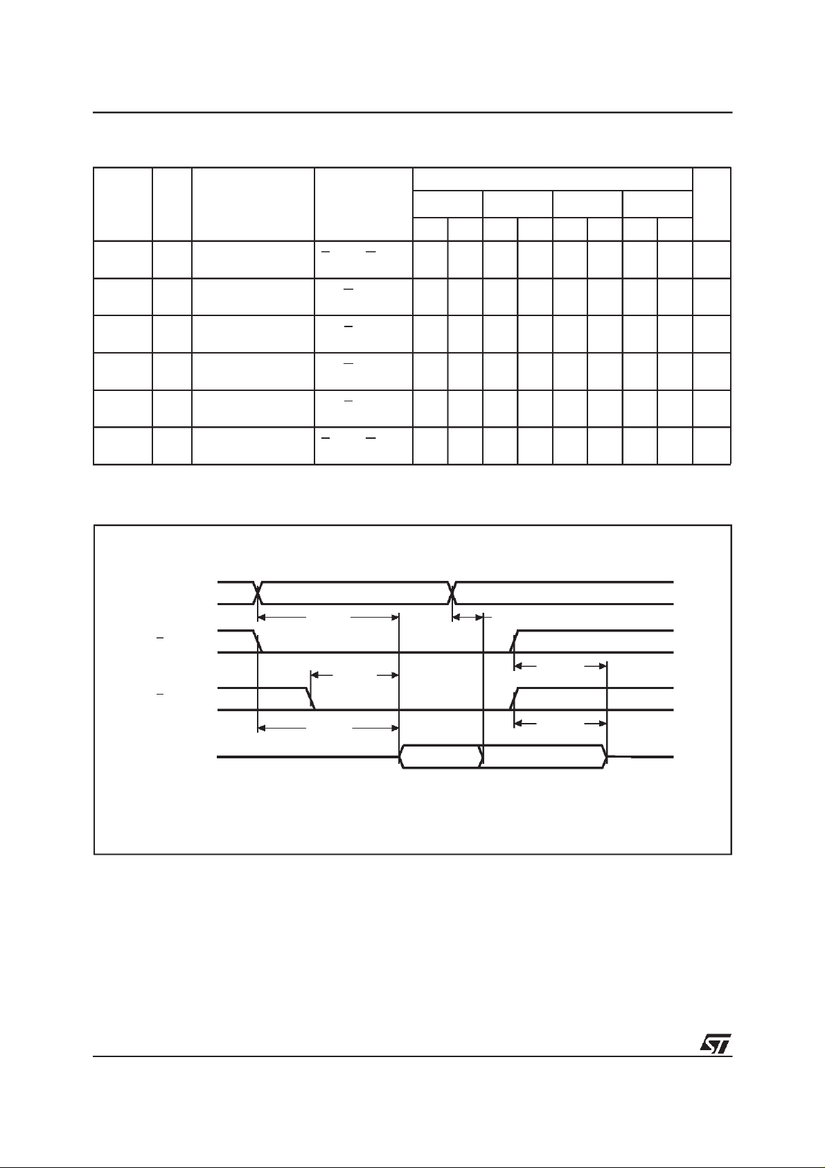
Table 8A. Read Mode AC Characteristics
Input Leakage Current 0V ≤ VIN≤ V
LI
Output Leakage Current 0V ≤ V
LO
Supply Current
Supply Current (Standby) TTL
Supply Current (Standby) CMOS
Program Current
PP
Input Low Voltage –0.3 0.8 V
IL
(2)
Input High Voltage 2
Output Low Voltage
OL
Output High Voltage TTL
OH
Output High Voltage CMOS
2. Maximum DC voltage on Output is V
CC
+0.5V.
(1)
E=V
= 0mA, f = 5MHz
I
OUT
E=V
E>V
V
PP=VCC
I
OL
I
OH
I
= –100µAV
OH
≤ V
OUT
,G=VIL,
IL
IH
– 0.2V
CC
= 2.1mA
= –1mA
CC
CC
3.6 V
– 0.7V
CC
±10 µA
±10 µA
30 mA
1mA
100 µA
10 µA
V
+1
CC
0.4 V
(TA= 0 to 70 °C, –40 to 85 °C or –40 to 125 °C; VCC=5V±5% or 5V ± 10%; VPP=VCC)
M27C512
Symbol Alt Parameter Test Condition
-45
(3)
Min Max Min Max Min Max Min Max
t
AVQVtACC
t
ELQV
t
GLQV
(2)
t
EHQZ
(2)
t
GHQZ
t
AXQX
Note: 1. VCCmust be applied simultaneously with or before VPPand removed simultaneously or after VPP.
2. Sampled only, not 100% tested.
3. Speed obtained with High Speed AC measurement conditions.
Address Valid to
Output Valid
Chip Enable Low to
t
CE
Output Valid
Output Enable Low
t
OE
to Output Valid
Chip Enable High to
t
DF
Output Hi-Z
Output Enable High
t
DF
to Output Hi-Z
Address Transition to
t
OH
Output Transition
E=V
E=V
,G=V
IL
G=V
E=V
G=V
E=V
,G=V
IL
IL
IL
IL
IL
IL
IL
45 60 70 80 ns
45 60 70 80 ns
25 30 35 40 ns
0 25 0 25 0 30 0 30 ns
0 25 0 25 0 30 0 30 ns
0000ns
-60 -70 -80
V
V
Unit
5/18
M27C512
Table 8B. Read Mode AC Characteristics
(1)
(TA= 0 to 70 °C, –40 to 85 °C or –40 to 125 °C; VCC=5V±5% or 5V ± 10%; VPP=VCC)
M27C512
Symbol Alt Parameter Test Condition
-90
-10 -12 -15/-20/-25
Min Max Min Max Min Max Min Max
t
AVQVtACC
t
ELQV
t
GLQV
(2)
t
EHQZ
(2)
t
GHQZ
t
AXQX
Note: 1. VCCmust be applied simultaneously with or before VPPand removed simultaneously or after VPP.
2. Sampled only, not 100% tested.
Address Valid to
Output Valid
Chip Enable Low to
t
CE
Output Valid
Output Enable Low
t
OE
to Output Valid
Chip Enable High to
t
DF
Output Hi-Z
Output Enable High
t
DF
to Output Hi-Z
Address Transition to
t
OH
Output Transition
E=V
E=V
,G=V
IL
G=V
E=V
G=V
E=V
,G=V
IL
IL
IL
IL
IL
IL
IL
90 100 120 150 ns
90 100 120 150 ns
40 40 50 60 ns
0 30 0 30 0 40 0 50 ns
0 30 0 30 0 40 0 50 ns
0000ns
Figure 5. Read Mode AC Waveforms
Unit
A0-A15
E
G
Q0-Q7
tAVQV
tELQV
VALID
tGLQV
VALID
tAXQX
tEHQZ
tGHQZ
Hi-Z
AI00735B
6/18
 Loading...