

1 Mbit Low Voltage Paged Flash Memory
With 20 MHz Serial SPI Bus Interface
■ 1 Mbit PAGED Flash Memory
■ 128 BYTE PAGE PROGRAM IN 3 ms TYPICAL
■ 256 Kbit SECTOR ERASE IN 1 s TYPICAL
■ BULK ERASE IN 2 s TYPICAL
■ SINGLE 2.7 V to 3.6 V SUPPLY VOLTAGE
■ SPI BUS COMPATIBLE SERIAL INTERFACE
■ 20 MHz CLOCK RATE AVAILABLE
■ SUPPORTS POSITIVE CLOCK SPI MODES
■ DEEP POWER DOWN MODE (1 µA TYPICAL)
■ ELECTRONIC SIGNATURE
■ 10,000 ERASE/PROG CYCLES PER SECTOR
■ 20 YEARS DATA RETENTI ON
■ –40 TO 85°C TEMPERATURE RANGE
DESCRIPTION
The M25P10 is an 1 Mbit Paged Flash M emory
fabricated with STMicroelectronics High
Endurance CMOS technology. The memory is
accessed by a simple SPI bus compatible serial
interface. The bus sign als are a s erial clock input
(C), a serial data input (D) and a serial data output
(Q).
The device connected to the bus is selected when
the chip select input (S
in during the low to high transition of clock C, data
) goes low. Data is clocked
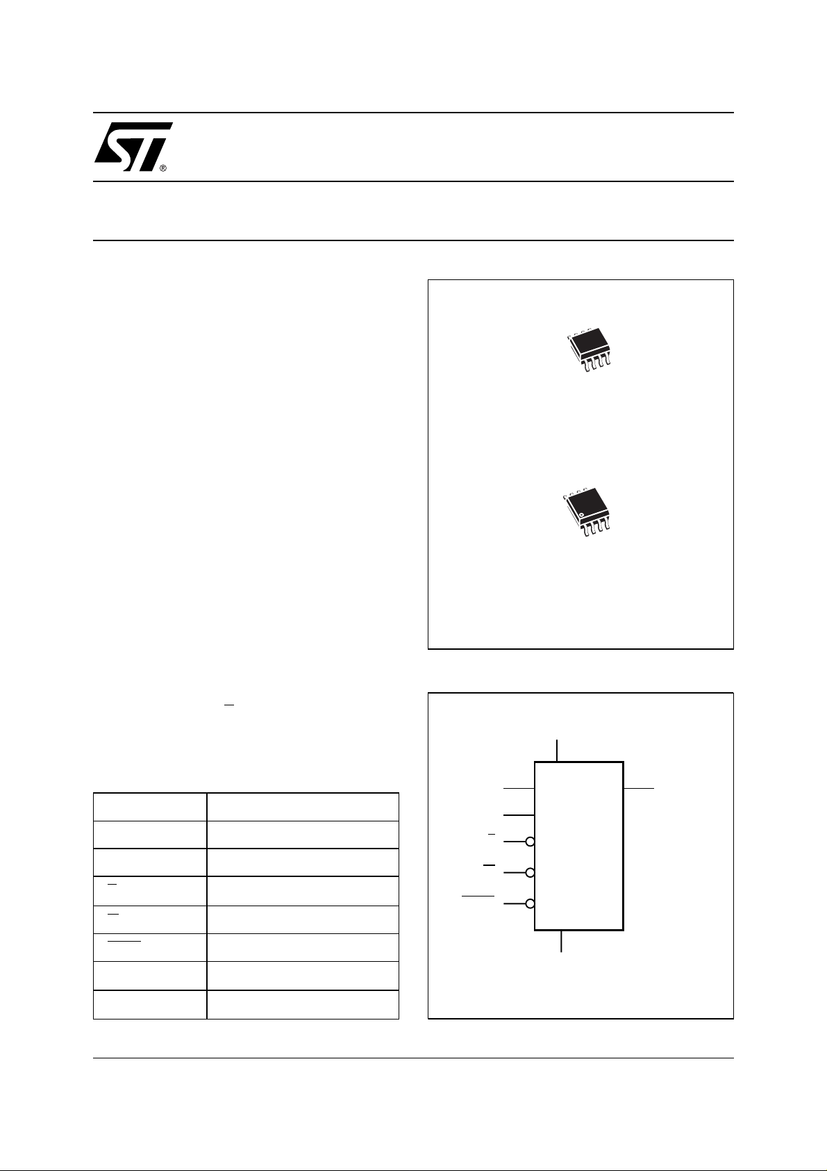
8
SO8 (MN)
150 mil width
8
SO8 (MW)
200 mil width
Figure 1. Logic Diagram
V
CC
M25P10
PRELIMINARY DATA
1
1
Table 1. Signal Names
C Serial Clock
D Serial Data Input
Q Serial Data Output
S
W
Write Protect
Hold
HOLD
V
CC
V
SS
June 2000
This is preliminary information on a new product now in development or undergoing evaluation. Details are subject to change without notice.
Chip Select
Supply Voltage
Ground
W
HOLD
D
C
S
M25P10
V
SS
Q
AI03744
1/21
M25P10
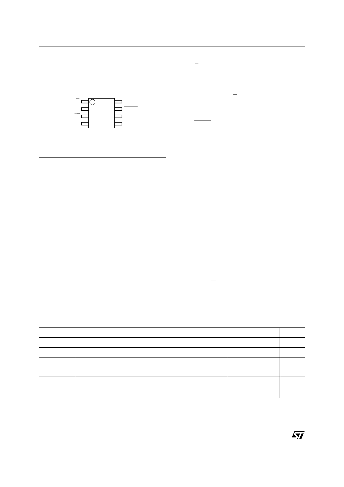
Figure 2. SO Connections
M25P10
1
SV
2
3
W
SS
4
8
7
6
5
AI03745
CC
HOLDQ
C
DV
is clocked out duri ng the high to low transition of
clock C
SIGNALS DESCRIPTION
Seria l O utput ( Q )
The output pin is used to transfer data serially out
of the memory. Data is shifted out on the falling
edge of the serial clock.
Serial Inpu t ( D )
The input pin is used to transfer data serially into
the device. It receives instructions, addresses,
and the data to be program med. Input is latched
on the rising edge of the serial clock.
Serial Clock (C)
The serial clock provides the timing of the serial
interface. Instructions, addresses, or data present
at the input pin are latched o n the rising edge of
the clock input, while data on the Q pin changes
after the falling edge of the clock input.
Chip Select (S
When S
is high, the memory is deselected and the
)
Q output pin is at high impedance a nd, unless an
internal Read, Program, Erase or Write Status
Register operation is underway, the device will be
in the Standby Power mode (this is not the Deep
Power Down mode). S
low enables the memory,
placing it in the active power mode. It should be
noted that after power-on, a high to low t ransition
is required prior to the start of any operation.
on S
Hold (HOLD
)
The HOLD pin is used to pause serial
communications with a SPI memory without
resetting the serial sequence. To take the Hold
condition into account, the product must be
selected. The HOLD condition is validated by a 0
state on the Hold pin synchronized with the 0 state
on the Clock, as shown in Figure 4. The DeHOLD
condition is validated by a 1 state on the Hold pin
synchronized with the 0 state on the Clock. During
the Hold condition D, Q, and C are at a high
impedance state.
When the memory is under HOLD condition, it is
possible to deselect the device. Then, the protocol
is reset. The memory remains on HOLD as long as
the Hold pin is Low. To restart communication with
the device, it is necessary t o both DeHOLD (H =
1) and to SELECT the memory.
Write Protect (W
)
This pin is for hardware write protection of the
Status Register (SR); except WIP and WEL bits.
When bit 7 (SRWD) of the status register is 0 (the
initial delivery state); it is possible to write the S R
once the WEL (Write Enable Latch) has been set
with the WREN instruction and whatever is the
status of pin W
(high or low).
Table 2. Absolute Maximum Ratings
Symbol Parameter Value Unit
T
A
T
STG
T
LEAD
V
IO
V
CC
V
ESD
Note: 1. Exc ept for the ratin g “Ambie nt Operati ng Temperat ure Range”, stresses abov e those liste d in this table may cause perman ent
2/21
damage to the dev ice. T hese are stress r atings only, a nd ope ration of the dev ice at t hese or any o ther co ndition s above those
indicated in the Operating se ctions of this s pecification is no t implied. Expos ure to Absolute M aximum Rating co nditions for
extended periods may affect device reliability. Refer also to the ST SURE Program and other relevant quality documents.
2. MIL -STD-883C, 3015.7 (1 00 pF, 1500 Ω)
Ambient Operating Temperature –40 to 85 °C
Storage Temperature –65 to 150 °C
Lead Temperature during Soldering SO8: 40 seconds 215 °C
Input and Output Voltage Range (with respect to Ground) –0.3 to 5.0 V
Supply Voltage Range –0.6 to 5.0 V
Electrostatic Discharge Voltage (Human Body model)
1
2
2000 V
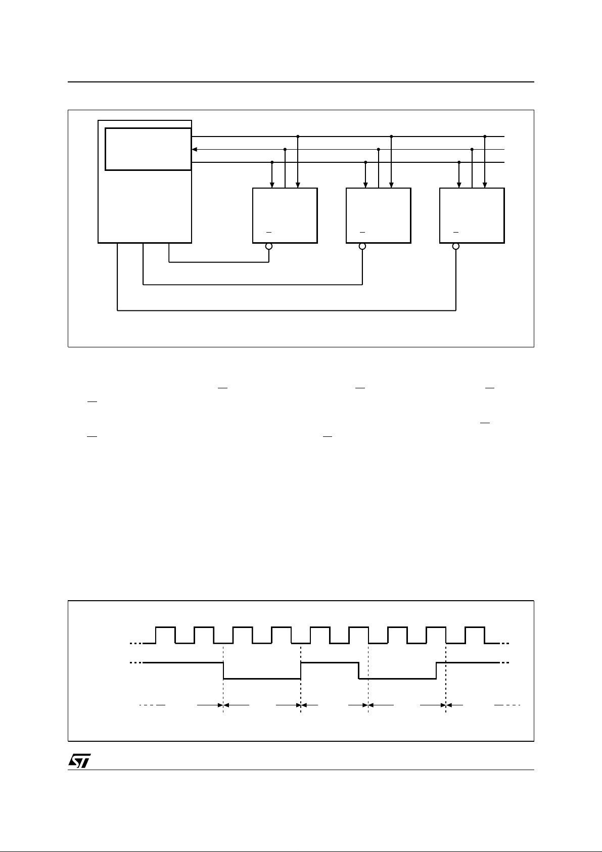
Figure 3. Microcontroller and Memor y Devices on the SPI Bus
M25P10
SPI Interface with
(CPOL, CPHA) =
('0', '0') or ('1', '1')
Master
(ST6, ST7, ST9,
ST10, Others)
CS3 CS2 CS1
SDO
SDI
SCK
CQD
M25P10
S
Once bit 7 (SRWD) of the status register has been
set to 1, the possibility to rewrite the SR depends
on the logical level present at pin W
pin is high, it will be possible to rewrite the
–If W
:
status register after having set t he WEL (Write
Enable Latch).
–If W
pin is low, any attempt to modify the status
register will be ignored by the device even if the
WEL was set. As a consequ ence: all the data
bytes in the memory area software protected
(SPM) by the BPi bits of the st atus register are
also hardware protected against data
modification and can be seen as a R ead Only
memory area. This mode is called the Hardware
Protected Mode (HPM).
CQD
M25P10
S
CQD
M25P10
S
AI03746
It is possible to enter the Hardware Protected
Mode (HPM) by setting SRWD bit after pulling
down the W
pin or by pulling down the W pin after
setting SRWD bit.
The only way to abort the Hardware Protected
Mode once entered is to pull high the W
pin is permanently tied to high level, the
If W
pin.
Hardware Protected Mode will never be activated
and the memory will only allow the user to
software protect a part of the memory with the BPi
bits of the status register.
All protection features of the device are
summarized in Table 3.
Figure 4. Hold Condition Activation
CLOCK
HOLD PIN
MEMORY
STATUS
ACTIVE
HOLD ACTIVE HOLD ACTIVE
AI02029B
3/21
M25P10
Figure 5. M25P10-Compatible SPI Modes
CPOL
CPHA
0
1
0
1
C
C
D or Q
MSB LSB
Clock Polarity (CPOL) and Clock Phase
(CPHA) with SPI Bus
As shown in Figure 5, th e M25 P10 can be driven
by a microcontroller with its SPI peripheral running
in either of the two following modes: (CPOL,
CPHA) = (’0’, ’0’) or (CPOL, CPHA) = (’1’, ’1’). For
these two modes, input data is latched in by the
low to high transition of clock C, and output data is
available from the high to low transition of Clock
(C).The difference between (CPOL, CPHA) = (0,
0) and (CPOL, CPHA) = (1, 1) is the clock polarity
when in stand-by: C remains at ’0’ for (CPOL,
CPHA) = (0, 0) and C remains at ’1’ for (CPOL,
CPHA) = (1, 1) when there is no data transfer.
MEMORY ORGANIZATION
The memory is organized in 131,072 words of 8
bits each. The device features 1,024 pages of 128
bytes each. Each page can be individually
programmed (bits are programmed from ‘1’ to ’0’
state).
AI01438
The device is also organized in 4 sectors of
262,144 bits (32,768 x 8 bits) each.The device is
Sector or Bulk Erasable but not Page Erasable
(bits are erased from ’0’ to ’1’ state).
OPERATIONS
All instructions, addresses and data are shifted in
and out of the chip MSB first. Data input (D) is
sampled on the first rising edge of clock (C) after
the chip select (S
) goes low. Prior to any
Table 4. Memory Organization
Sector Address Range
3 18000h 1FFFFh
2 10000h 17FFFh
1 08000h 0FFFFh
0 00000h 07FFFh
Table 3. Protection Features
W SRWD Status Register (SR)
X 0 Writeable after setting WEL
1 1 Writeable after setting WEL
0 1 Hardware protected
Note: 1. SPM: Software Pr otected Mode.
2. HPM: Hardware Protected Mode.
3. BPi: Bits BP0 and BP1 of the Status Register.
4. WEL: Wri te Enable Latch of the Sta tus Register.
5. W
: Write Protect Input Pin.
6. SRWD: Status Register Wri te Disable Bits of the St at us Register.
7. The device is Bulk Er asable if, and only if, (BP0, BP1) = (0, 0), (see Bulk Er ase paragraph).
4/21
Data Bytes (Software
Protected Area by BPi bits)
Software protected by the BPi
bits of the Status Register
Software protected by the BPi
bits of the Status Register
Hardware protected by the
BPi bits of the Status Register
and the W
pin
Mode
SPM
SPM
HPM
Data Bytes (Unprotected
Area)
Paged Programmable and
Sector Erasable
Paged Programmable and
Sector Erasable
Paged Programmable and
Sector Erasable
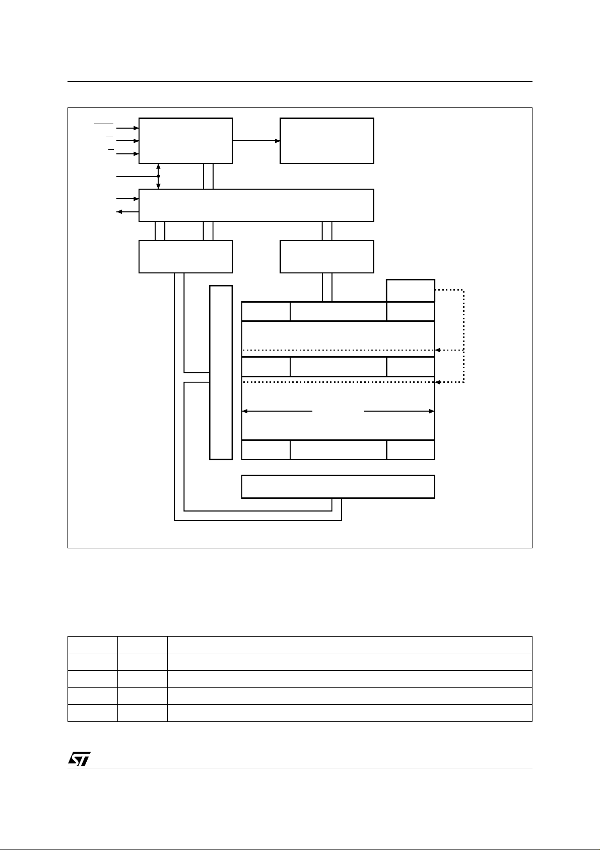
Figure 6. Block Diagram
M25P10
HOLD
W
S
C
D
Q
Control Logic
I/O Shift Register
Address Register
and Counter
Y Decoder
High Voltage
Generator
Data
Register
128 Bytes
Status
1FFFFh1FF80h
An + 7FhAn
Size of the
Read only
Memory
area
X Decoder
Table 5. Protected Area Sizes
BP1 BP0 Software Protected Area
0 0 none
0 1 Upper quarter = Sector 3
1 0 Upper half = Sectors 2 & 3
1 1 Whole memory= Sectors 0, 1, 2 & 3
007Fh0000h
AI03747
5/21
M25P10
Table 6. Instruction Set
Instruc
tion
WREN Set Write Enable Latch 0000 0110
WRDI Reset Write Enable Latch 0000 0100
RDSR Read Status Register 0000 0101
WRSR Write Status Register 0000 0001
READ Read Data from Memory Array 0000 0011
PP
SE
BE
DP Enter Deep Power-down mode 1011 1001
RES
Program up to 128 Data bytes
to Memory Array
Sector Erase (set to FFh) one
sector of Memory Array
Bulk Erase (set to FFh) whole
of Memory Array
Release from Deep Powerdown mode, and Read
Electronic Signature
Description
Instruction
Format
0000 0010
1101 1000
1100 0111
1010 1011
operation, a one-byte instruction code must be
sent to the chip. This c od e is entered via the dat a
input (D), and latched on the rising edge of the
clock input (C). To enter an instruction code, the
device must have bee n previously selected (S
=
low). Table 6 shows the available instruction set.
At Power-up and Power-down, the device must
not be selected (that is the S
voltage applied on the V
voltage reaches the correct V
(min) at Power-up and VSS at Power-down (a
V
CC
simple pull-up resistor on S
input must follow the
pin) until the supply
CC
values which are
CC
insures safe and
proper power up and down phases).
Read Data Byte(s) (READ)
The device is first selected by putting S
low. Th e
Read instruction byte is followed by a three bytes
address (A23-A0), each bit being latched-in during
the rising edge of the clock (C). Then the data
stored in the memory at the selected byte address
is shifted out on the Q output pin, each bit being
shifted out during the falling edge of the clock (C).
The first byte a ddressed can be any byt e within a
page. The address is automatically incremented to
the next higher address after each byte of dat a is
shifted out. The whole memory can theref ore be
read with a single Read instruction. When the
highest address is reached, the add ress counter
rolls over to 000000h allowing the read cycle to be
continued indefinitely.
The Read operation is terminated by deselecting
the chip. The chip can be deselec ted at any time
during data output. Any read attempt during an
Erase, Program or Write Status Register cycle will
be rejected and will deselect the chip without
having any effects on the ongoing operation.
The timing sequence is shown in Figure 11.
Page Program (PP)
Prior to any Page Program attempt, a write enable
instruction (WREN) must have been previously
sent (the S
properly transmitted and the S
input driven low, WREN instruction
input driven high).
After the WREN instruction decoding, the memory
sets the Write Enable Latc h (WEL) which allows
the execution of any further Page Program
instruction. The Page Program instruction is
entered by driving the Chip select input (S
) low,
followed by the instruction byte, 3 address bytes
and at least 1 data byte on Data In input (D). If the
least significant address bits differ from [A6A0]=000.0000, all transmi tted data ex ceeding the
addressed page boundary will roll over and will be
programmed from address [A6-A0]=000.0000 of
this same page. The Chip Select input (S
) must be
driven low for the entire duration of the sequence.
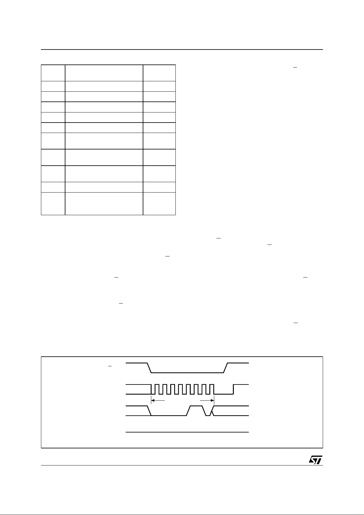
Figure 7. WREN: Set Write Enable Latch Sequence
S
21 34567
0
C
INSTRUCTION
D
HIGH IMPEDANCE
Q
6/21
AI02281B
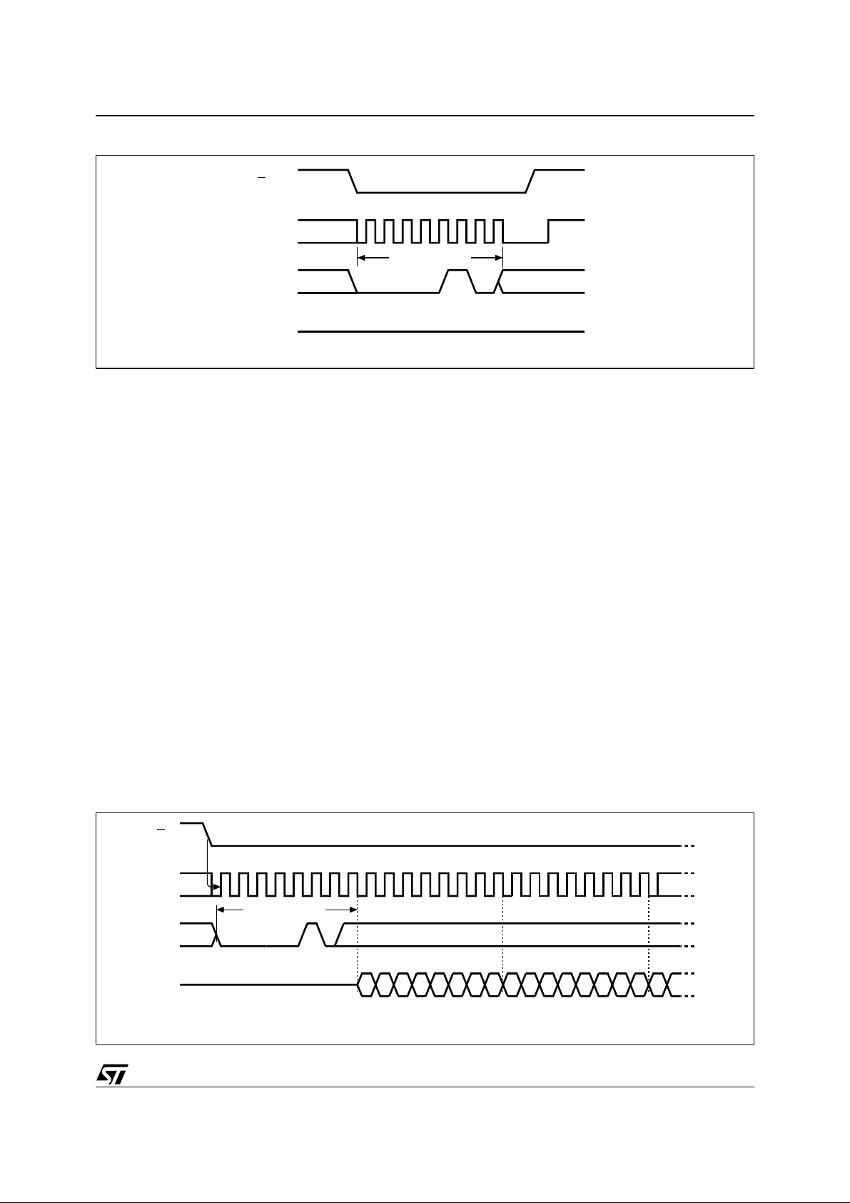
Figure 8. WRDI: Reset Write Enable Latch Sequence
S
21 34567
0
C
INSTRUCTION
D
HIGH IMPEDANCE
Q
M25P10
AI03750
If more than 128 bytes are sent to the device,
previously latched data are discarded and the last
128 data bytes are guaranteed to be programmed
correctly within the s ame page. If less than 128
Data bytes are sent to device; they are correctly
programmed at the requested addresses without
having any effects on the other bytes of the same
Page.
The device must be deselected just after the
eighth bit of the last data byte has been latched in.
If not, the Page Program instruction is not
executed. As soon as the device is deselected, the
self-timed Page Program cycle (t
) is initiated.
PP
While the Page Program cycle is in progress, the
status register may be read to check the WIP bit
value. WIP is high during the self-timed Page
Program cycle and is low when it is completed.
When the cycle is completed, the write enable
latch (WEL) is reset.
A Page Program instruction applied to a Page
which is software protected by the BPi bits (see
Table 4 and Table 5) is not initiated.
Figure 9. RDSR: Read Status Register Sequence
The timing sequence is shown in Figure 12.
Write Enable (WREN) and Write Disable (WRDI)
The Write Enable Latch must be set prior to every
Page Program (PP), Sector Erase (SE), Bulk
Erase (BE) and Write Status Register (WRSR)
operation. The WREN instruction, whose timing
sequence is sho wn in Figure 7, w ill set the latch
and the WRDI instruction, whose timing sequence
is shown in Figure 8, will reset the latch.
The Write Enable Latch is reset under the
following conditions:
– Power on
– WRDI instruction completion
– WRSR in s t ru ctio n completio n
– Page Program instruction completion
– Sector Erase instruction completion
– Bulk Erase instruction completion.
After completion of either WREN or WRDI
instruction, the chip enters a wait state and waits
for a deselect.
S
21 3456789101112131415
0
C
INSTRUCTION
D
Q
HIGH IMPEDANCE
STATUS REG. OUT
7 6543210
MSB
STATUS REG. OUT
7 6543210
MSB MSB
7
AI02031
7/21

M25P10
Figure 10. WRSR: Write Status Register Sequence
S
21 3456789101112131415
0
C
INSTRUCTION STATUS REG.
D
HIGH IMPEDANCE
Q
Read Status Register (RDSR)
The RDSR instruction provides access to the
Status Register content. The Status Register may
be read at any time, even during a Page Program,
Sector Erase, Bulk Erase or Write Status Register.
When one of these instructions is in progress, it is
recommended to check the WIP bit before sending
a new instruction to the device. For this, it is
possible to continuously read the Status Register
value.
WIP bit: The Write-In-Process (WIP) bi t indicates
whether the memory is busy with a Write Status
Register, Program or Erase operation. When set
to a ’1’, such an operation is in progress, when set
to a ’0’ no such operation is in progress.
765432 0
MSB
1
AI02282
WEL bit: The Write Enable Latch (WEL) bit
indicates the status of the internal Write Enable
Latch. When set to a ’1’ t he latc h is set, when set
to a ’0’ the latch is reset and no Write Status
Register, Program or Erase sequence will be
allowed.
BP1,BP0 bits: The Block Protect bits BPi are nonvolatile bits. They define the size of the area to be
software protected against Program and Erase
operations. These bits a re written with the WRSR
instruction (see Table 5). Once (BP0, BP1) are set
to a value different from (0,0), the relevant area
becomes protected against Page Program and
Sector Erase operations. B Pi bits can be written
provided that the Hardware Protected Mode has
not been set. The Bulk Erase instruction is
Figure 11. READ: Read Data Bytes Sequence
S
21 345678910 2829303132333435
0
C
INSTRUCTION 24 BIT ADDRESS
23
D
HIGH IMPEDANCE
Q
Note: 1. Address bits A23 to A17 are Don’t Care on the M25P10 series.
8/21
2221 3210
36 37 38
DATA OUT
765432 0
MSB
1
AI03748

M25P10
Table 7. Status Register Format
b7 b0
SRWD 0 0 0 BP1 BP0 WEL WIP
Note: 1. SRWD, BP0 and BP1 are non-volatile read and write bits.
2. WEL and WIP are volatile r ead-only bits (WEL is set and
reset by specific instructions; WIP is automatically set
and reset by the internal logic of the device).
internally taken into account if, and only if, (BP0,
BP1) = (0,0).
SRWD bit : The SRWD bit operates together with
pin. SRWD bit an d W pin allow the p art to
the W
be put in the Hardware protected mode. In this
mode (W
pin = 0 and SRWD = 1), the non-volatile
bits of the Status Register (SRWD, BP1, BP0)
become read only bits and the Write Status
Register (WRSR) instruction has no more effect
on the device (please see the section entitled
“Write Protect (W)” on page 2, and Table 3).
Write in the Status Register (WRSR)
Prior to any WRSR instruction, a write enable
instruction (WREN) must have been previously
sent (the S
properly transmitted and the S
input driven low, WREN instruction
input driven high).
After the WREN instruction decoding, the memory
sets the Write Enable Latc h (WEL) which allows
the execution of any further WRSR instruction.
The WRSR instruction is entered by driving the
Chip select input (S
) low, followed by the
instruction byte and the data byte on Data In input
(D). WRSR instruction has no effect on b6, b5, b4,
b1 and b0 of the Status Register. b6, b5 and b4 are
always read at ’0’.
The device must be deselected just after the
eighth bit of the d ata byte has been latched in. If
not, the WRSR instruction is not executed. As
soon as the device is deselected, the self-timed
Write Status Register cycle (t
) is initia ted. W hile
W
the Write Status Register cycle is in prog ress, t he
Status Register may still be read to check the WIP
bit value. WIP is high during the s elf-timed Write
Status Register cycle and is low when it is
completed. When the cycle is completed, the write
enable latch (WEL) is reset.
The WRSR instruction allows the user to define
the size of the software Protected area (Read
Only) when setting the BP1,BP0 values, according
to Table 4. The WRSR instruction also allows the
user to set or reset the SRWD bit in accordance
with the W
pin. SRWD bit and W pin allow the part
to be put in the Hardware protected mode (please
see the sections entitled “Read Status Register
(RDSR)” on page 8, “Write Protect (W)” on page 2,
and Table 3). WRS R instruction has no effect on
Figure 12. P P: Page Program Sequ e nce
S
21 345678910 2829303132333435
0
C
INSTRUCTION 24 BIT ADDRESS
D
S
4241 43 44 45 46 47 48 49 50 52 53 54 5540
C
DATA BYTE 2
D
765432 0
1
23
2221 3210
51
DATA BYTE 3
765432 0
1
36 37 38
DATA BYTE 1
765432 0
1050
1051
1052
1049
DATA BYTE 128
65432 0
1053
1
1
1054
39
1055
AI03749
Note: 1. Address bits A2 3 to A17 are D on’ t Care on the M 25P10 series.
9/21

M25P10
Figure 13. SE: Sector Erase Sequence
S
21 3456789 293031
0
C
INSTRUCTION
D
Note: 1. Address bits A2 3 to A17 are D on’ t Care on the M 25P10 series.
23 22 2 0
MSB
the device once the Hardware Protected Mode is
entered.
The timing sequence is shown in Figure 10.
Sector Erase (SE)
Prior to any Se ctor Erase at tempt, a write enab le
instruction (WREN) must have been previously
sent (the S
properly transmitted and the S
input driven low, WREN instruction
input driven high).
After the WREN instruction decoding, the memory
sets the Write Enable Latc h (WEL) which allows
the execution of any further Sector Erase. The
Sector Erase instruction is entered by driving t he
Chip select input (S
) low, followed by the
instruction byte and 3 address bytes on Data In
input (D). Any address of the Sector (see Table 4)
is a valid address for the Sector Erase instruction.
The Chip Select input (S
) must be driven low for
the entire duration of the sequence. The device
must be deselected just after t he eighth b it of the
24 BIT ADDRESS
1
AI03751
last address byte has been latched i n. If not, the
Sector Erase instruction is not executed. As soon
as the device is deselected, the self -timed Sector
Erase cycle (t
) is initiated. While the Sector
SE
Erase cycle is in progress, the status register may
be read to check the W IP bit value. WIP is high
during the self-timed Sector Erase cycle and is low
when it is completed. When the cycle is
completed, the write enable latch (WEL) is reset.
A Sector Erase instruction applied to a Sector
which is software protected by the BPi bits (see
Table 4 and Table 5) is not initiated.
The timing sequence is shown in Figure 13.
Bulk Erase (B E)
Prior to any Bulk Erase attempt, a write enable
instruction (WREN) must have been previously
sent (the S
properly transmitted and the S
input driven low, WREN instruction
input driven high).
After the WREN instruction decoding, the memory
Figure 14. BE: Bulk Erase Sequence
S
C
D
10/21
21 345670
INSTRUCTION
AI03752

M25P10
Figure 15. DP: Enter Deep Power Down Mode Sequence
S
21 345670
C
INSTRUCTION
D
tDP
Deep Power Down Mode
is high, the memory is
CC1
to I
(see Table 10).
CC2
AI03753
sets the Write Enable Latc h (WEL) which allows
the execution of any further Bulk Erase. The Bulk
Erase instruction is entered by driving the Chip
select input (S
) low, followed by the instruction
byte on Data In input (D).
The Chip Select input (S
) must be driven low for
the entire duration of the sequence. The device
must be deselected just after t he eighth b it of the
instruction byte has been latched in. If not, the
Bulk Erase instruction is not executed. As soon as
the device is deselected, the self-timed Bulk Erase
cycle (t
) is initiated. While the Bulk Erase cycle
BE
is in progress, the status register m ay be read to
check the WIP bit value. WIP is high during the
self-time d Bulk E rase cycle and is lo w when it is
completed. When the cycle is completed, the write
enable latch (WEL) is reset.
The Bulk Erase instruction is interna lly taken into
account if, and only if, (BP0, BP1) = (0,0). In other
Stand-by Power Down Mode
words, the Bulk Erase instruction i s ignored if at
least one Sector is software protected. In this case
the Bulk Erase instruction is discarded and none of
the Sectors are erased.
The timing sequence is shown in Figure 14.
Enter Deep Pow er D ow n Mode (DP)
After Power-on, when S
deselected, the Q output pin is at high impedance
and the device is in the Standby Power Mode state
). Under this state, the Memory waits for a
(I
CC1
select condition and is able to receive, decode and
execute all instructions.This mode is not the Deep
Power Down Mode which is entered by the way of
a specific instruction. The purpose of the Deep
Power down mode is to drastically reduce the
standby current from I
Once the device has entered the Deep Power
Down Mode, all instructions are ignored except the
RES instruction which releases the part from this
Figure 16. RES: Release from Deep Power Down Mode and Read Electronic Signature Sequence
S
C
D
Q
11/21
21 345678910 2829303132333435
0
INSTRUCTION 24 BIT ADDRESS
23
2221 3210
HIGH IMPEDANCE
MSB
36 37 38
DATA OUT (Electronic Signature)
765432 0
Deep Power Down Mode
1
Stand-by Power Down Mode
AI03755

M25P10
Figure 17. RES: Release from Deep Power Down Mode Sequence
S
21 345670
C
INSTRUCTION
D
HIGH IMPEDANCE
Q
tRES
mode. At the same time, the RES instruction
provides the Electronic Signature of the device on
the Q output pin. At power down, the Deep Down
Mode is automatically discarded. Thi s causes the
device to always wake up in the Standby Power
Mode state after power-on.
The DP instruction is entered by driving the Chip
select input (S
) low, followed by the instruction
byte on Data In input (D). The Chip Select input (S
must be driven low f or the entire duration of the
sequence. The device must be deselected just
after the eighth bit of the instruction byte has been
latched in. If not, the DP instruction is not
executed. As soon as the device is deselected, it
requires t
where standby current is reduced to I
to enter the Deep Power Down Mode
DP
CC2
.
The timing sequence is shown in Figure 15.
Release from Deep Power Down Mode and
Read Electronic Signature (RES)
Once the device has entered the Deep Power
Down Mode, all instructions are ignored except the
RES instruction which releases the part from this
mode. At the same time, the RES instruction
provides the Electronic Signature of the device on
the Q output pin. Except during an Erase, Program
cycle or Write Status register, the RES instruction
always provides access to the Electronic
Signature of the device and can be applied even if
the Deep Power Down Mode has not been
entered. Any RES attempt during an Erase,
Program cycle or Write Status register, will be
rejected and will desel ect the chip without having
any effects on the ongoing Erase, Program cycle
or Write Status Register.
Deep Power Down Mode
Stand-by Power Down Mode
The device is first selected by putting S
RES instruction byte is followed by a dummy three
bytes address (A23-A0), each b it being latched-in
on Data In input (D) during the rising edge of the
clock (C). Then, the Electronic Signature stored in
the memory is shifted out on the Q output pin,
each bit being shifted out during the falling edge of
the clock (C). It is possible to continuously read the
Electronic Signature value. The RES operation is
)
terminated by deselecting the chip after the
Electronic Signature has been read at least one
time (see Figure 16). At this step, the device is
immediately put again in the Standby Power Mode
state. It waits for a select cond ition and i s able t o
receive, decode and execute all instructions.
Deselecting the device after the 8 bits RES
instruction has been sent but before the LSB of the
Electronic Signature has been read, will insure the
Deep Power Down Mo de to be released but will
generate a delay (t
) before the device is put in
RES
Standby Power Mode state (see Figure 17) and S
must remain high for at least t
max value (see
RES
Table 13).
POWE R O N STATE
At Power-up, the device must not be selected (that
is the S
the V
minimum V
input must follow th e voltage sup plied on
pin) until the supply voltage reaches the
CC
value (2.7 V). Once VCC has
CC
reached the minimum operating voltage (2.7 V),
the Chip Select input pin (S
a time higher than t
VSL
) must remain high for
min (See Table 8).
After a Power up, the m emory is in the following
state:
AI03754
low. Th e
12/21

M25P10
Table 8. Power-Up Timing and VWI Threshol d
(T
= –40 to 85 °C)
A
Symbol Parameter Test Condition Min. Max. Unit
1
I
VSL
I
PUW
V
Note: 1. These paramet ers are characterize d onl y.
VCC(min) to S low
1
Time delay to Write operation 15 ms
1
Write Inhibit Voltage 1.5 2.5 V
WI
10 µs
– The device is in the low power standby state
(not the Deep Power Down Mode).
– The chip is deselected.
– The Write Enable Latch is reset.
POWER UP OPERATION
In order to prevent data corruption and inadvertent
Page Program, Erase or Write Status Register
operations, an internal V
these features if the V
comparator inhibits all
CC
voltage is lower than V
CC
WI
(see Table 8).
Once the voltage applied on the V
the V
threshold (VCC>VWI):
WI
pin goes over
CC
– Page Program, Erase and Write Status Register
operations are allowed after a time-out of t
PUW
as specified in Table 8.
– This time-out delay allows the voltage applied
on V
pin to reach VCC(min) of the device. It
CC
should be noted that none of the device's
operation are guaranteed till V
V
(min).
CC
is not ≥
CC
DATA PROTECTION AND PROTOCOL
CONTROL
Once all bits of a Page Program, Sector Erase,
Bulk Erase or Status Register Write instruction are
received; the S
input must be driven high
(Deselect) right after the proper clock count in
order to execute the instruction, that is the Chip
Select S
must driven high after a clock pulses
count multiple of 8 bit.
Attempting to access the memory array during a
Write, Program or Erase cycle is ignored, however
the internal cycle continues.
Table 9. Initial Status Register Format
b7 b0
0 0000000
Status Register content is 00h (all Status Register
bits are ’0’).
,
ELECTRONIC SIGNATURE
The device features an 8 bits Electronic Signature
(10h) which can be read with the help of the RE S
instruction (please see the section entitled
“Release from Deep Power Down Mode and Read
Electronic Signature (RES)” on page 12).
INITIAL DELIVERY STATE
The device is delivered with the memory array
erased: all bits are set at ’1’ (each byte = FFh). The
13/21

M25P10
Table 10. DC Characteristics
(T
= –40 to 85 °C; VCC = 2.7 to 3.6 V)
A
Symbol Parameter Test Condition Min. Max. Unit
I
Input Leakage Curren t ± 2 µA
LI
I
I
I
I
I
I
I
I
V
V
V
Output Leakage Current ± 2 µA
LO
Stand-by mode Current S = VCC, V
CC1
S
Deep Power Down Current
CC2
Operating Current (READ)
CC3
Operating Current (PP)
CC4
Operating Current (WRSR)
CC5
Operating Current (SE)
CC6
Operating Current (BE) S = V
CC7
Input Low Voltage – 0.6 0.3V
IL
Input High Voltage 0.7V
IH
Output Low Voltage
OL
= VCC, V
C = 0.1V
= VSS or V
IN
= VSS or V
IN
/ 0.9.VCC at 20 MHz,
CC
Q = open
S
= V
CC
S
= V
CC
S
= V
CC
CC
I
= 1.6 mA
OL
CC
CC
CC
50 µA
5µA
3mA
15 mA
15 mA
15 mA
15 mA
CC
VCC+1 V
0.4 V
V
V
Output High Voltage IOH = –100µAV
OH
Table 11. Input Parameters
1
(TA = 25 °C, f = 20 MHz)
–0.2 V
CC
Symbol Parameter Test Condition Min. Max. Unit
C
OUT
C
IN
Note: 1. Sampled only, not 100% tested.
Table 12. AC Measurement Conditions
Input Rise and Fall Times
Input Pulse Voltages
Input and Output Timing
Reference Voltages
Output Load
Note: 1. Outpu t Hi -Z is de fin ed as t he poi nt w here d at a out is n o
longer driven.
Output Capacitance (Q) 8 pF
Input Capacitance (other pins) 6 pF
Figure 18. AC Testing Input Output Waveforms
5ns
0.2V
0.3V
≤
CC
CC
C
= 30 pF
L
to 0.8V
to 0.7V
CC
CC
0.8V
0.2V
CC
CC
0.7V
0.3V
AI00825
CC
CC
14/21

Table 13. AC Characteristics
Symbol Alt. Parameter
M25P10
V
=2.7 to 3.6 V
CC
T
=–40 to 85°C
A
Min Max
M25P10
Unit
f
C
t
SLCH
t
CHSL
1
t
CH
1
t
CL
t
DVCH
t
CHDX
t
CHSH
t
SHCH
t
SHSL
2
t
SHQZ
t
CLQV
t
CLQX
t
HLCH
t
CHHH
t
HHCH
t
CHHL
2
t
HHQX
2
t
HLQZ
2
t
DP
2
t
RES
t
W
t
PP
t
SE
t
BE
Note: 1. tCH + tCL ≥ 1 / fC.
2. Value guaranteed by characterization, not 100% tested in production. These parameters are specified with an output load
capacitance of 30 pF.
t
CSS
t
CLH
t
CLL
t
DSU
t
t
CSH
t
DIS
t
t
t
f
DH
t
HO
LZ
HZ
C
Clock Frequency D.C. 20 MHz
S Active Setup Time (relative to C) 10 ns
S Not Active Hold Time (relative to C) 10 ns
Clock High Time 22 ns
Clock Low Time 22 ns
Data In Setup Time 5 ns
Data In Hold Time 5 ns
S Active Hold Time (relative to C) 10 ns
S Not Active Setup Time (relative to C) 10 ns
S Deselect Time 50 ns
Output Disable Time 20 ns
V
Clock Low to Output Valid 20 ns
Output Hold Time 0 ns
HOLD Setup Time (relative to C) 10 ns
HOLD Hold Time (relative to C) 10 ns
HOLD Setup Time (relative to C) 10 ns
HOLD Hold Time (relative to C) 10 ns
HOLD to Output Low-Z 20 ns
HOLD to Output High-Z 20 ns
S High to Deep Power Down Mode 1.6
S High to Stand-by Power Mode 1.6
Write Status Register Cycle Time 5 ms
Page Program Cycle Time 5 ms
Sector Erase Cycle Time 2 s
Bulk Erase Cycle Time 4 s
s
µ
s
µ
15/21

M25P10
Figure 19. Serial Input Timing
S
C
tDVCH
tSLCH
tSHSL
tCHSHtCHSL
tSHCH
tCHCL
D
Q
Figure 20. Hol d Timing
S
C
Q
D
tCHDX
MSB IN
HIGH IMPEDANCE
tCHHL
tCLCH
LSB IN
tDLDH
tDHDL
AI01447
tHLCH
tHHCH
tCHHH
tHHQXtHLQZ
HOLD
Figure 21. Output Timing
S
C
tCLQX
Q
ADDR.LSB IN
D
16/21
tCLQV
tCH
tCL
tQLQH
tQHQL
AI02032
tSHQZ
LSB OUT
AI01449B

M25P10
Table 14. Ordering Information Scheme
Example: M25P10 –V MW 6 T
Memory Capacity Option
10 1 Mbit (128K x 8) T Tape and Reel Packing
Temperature Range
6 –40 °C to 85 °C
Operating Voltage Package
V 2.7 V to 3.6 V MN SO8 (150 mil width)
MW SO8 (200 mil width)
ORDERING INFORMATION
The notation used for the device number is as
shown in Table 14. For a list of available options
(speed, package, etc.) or for further information on
any aspect of this device, please contact your
nearest ST Sales Office
.
17/21

M25P10
Table 15. SO8 - 8 lead Plastic Small Outline, 150 mils body width
Symb.
Typ. Min. Max. Typ. Min. Max.
A 1.35 1.75 0.053 0.069
A1 0.10 0.25 0.004 0.010
B 0.33 0.51 0.013 0.020
C 0.19 0.25 0.007 0.010
D 4.80 5.00 0.189 0.197
E 3.80 4.00 0.150 0.157
e 1.27 – – 0.050 – –
H 5.80 6.20 0.228 0.244
h 0 .25 0.50 0.010 0.020
L 0 .40 0.90 0.016 0.035
α
N8 8
CP 0.10 0.004
mm inches
0° 8° 0° 8°
Figure 22. SO8 narrow (MN)
B
SO-a
Note: 1. D rawing is not to scale.
h x 45˚
A
e
D
N
1
CP
E
H
C
LA1 α
18/21

Table 16. SO8 - 8 lead Plastic Small Outline, 200 mils body width
Symb.
Typ. Min. Max. Typ. Min. Max.
A 2.03 0.080
A1 0.10 0.25 0.004 0.010
A2 1.78 0.070
B 0.35 0.45 0.014 0.018
C 0.20 – – 0.008 – –
D 5.15 5.35 0.203 0.211
E 5.20 5.40 0.205 0.213
e 1.27 – – 0.050 – –
H 7.70 8.10 0.303 0.319
L 0 .50 0.80 0.020 0.031
α
N8 8
CP 0.10 0.004
mm inches
0° 10° 0° 10°
M25P10
Figure 23. SO8 wide (MW)
B
Note: 1. D rawing is not to scale.
N
1
SO-b
A2
e
D
CP
E
H
A
C
LA1 α
19/21

M25P10
Table 17. Revision History
Date Description of Revision
24-Feb-2000
30-May-2000 Title changed from “Paged Non-Volatile Memory” to “Paged Flash Memory”
Document reformatted in preparation for full release; no parameters changed except data retention,
which has been changed to 20 years.
20/21

M25P10
Information furnished is believed to be accurate and reliable. However, STMicroelectronics assumes no responsibility for the consequences
of use of such information nor for any infringement of patents or other rights of third parties which may result from its use. No license is granted
by implic ation or otherwise under any patent or p atent rights of STMi croelectr oni cs. Spec i fications mentioned i n this publicatio n are subject
to change without notice. This publication supersedes and replaces all information previously supplied. STMicroelectronics products are not
authorized for use as cri tical comp onents in life support dev i ces or systems wi t hout expres s written approval of STMi croelectr o nics.
© 2000 STMicroelectronics - All Rights Reserved
The ST logo is a registered trademark of STMicroelectr oni cs.
All other na m es are the prop erty of their respectiv e owners.
STMicroelectronics GROUP OF COMPANIES
Australia - Brazil - China - Finland - France - Germany - Hong Kong - India - Italy - Japan - Malaysia - Malta - Morocco - Singapore - Spain -
Sweden - Switzerland - United K i ngdom - U.S. A.
http://www.st.com
21/21
 Loading...