

Datasheet M24C02-S, M24C04-S, M24C08-S, M24C02-L, M24C01-S Datasheet (SGS Thomson Microelectronics)
...
1/26May 2003
M24C16, M24C08
M24C04, M24C02, M24C01
16Kbit, 8Kbit, 4Kbit, 2Kbit and 1Kbit Serial I²C Bus EEPROM
FEATURES SUMMARY
■ Two Wire I
2
C Serial Interface
Supports 400 kHz Protocol
■ Single Supply Voltage:
– 4.5V to 5.5V for M24Cxx
– 2.5V to 5.5V for M24Cxx-W
– 2.2V to 5.5V for M24Cxx-L
– 1.8V to 5.5V for M24Cxx-R
■ Write Control Input
■ BYTE and PAGE WRITE (up to 16 Bytes)
■ RANDOM and SEQUENTIAL READ Modes
■ Self-Timed Pro gr amming Cyc le
■ Automatic Address Incrementing
■ Enhanced ESD/Latch-Up Behavior
■ More than 1 Million Erase/Write Cycles
■ More than 40 Year Data Retention
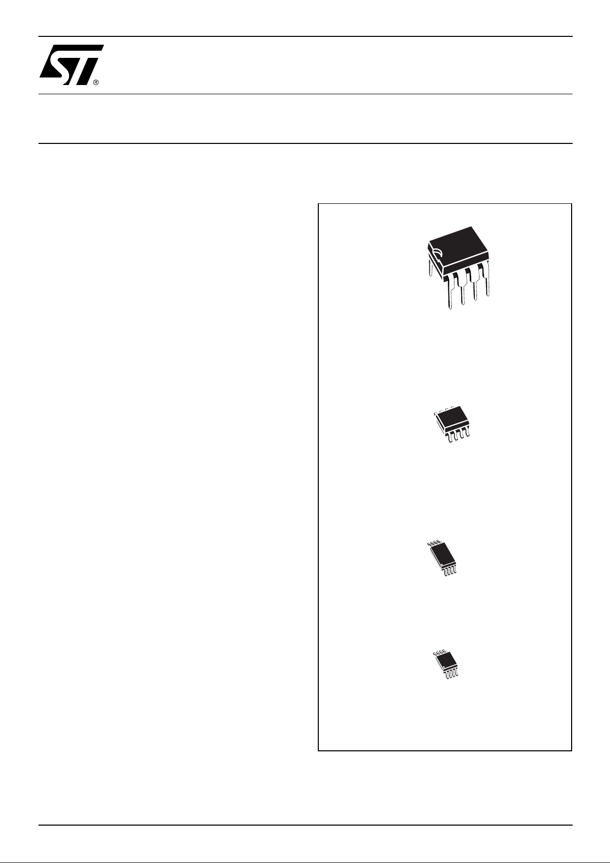
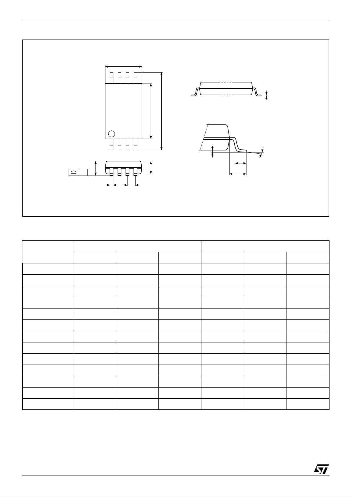
Figure 1. Packages
PDIP8 (BN)
8
1
SO8 (MN)
150 mil width
8
1
TSSOP8 (DW)
169 mil width
TSSOP8 (DS)
3x3mm² body size (MSOP)
M24C16, M24C08, M24C04, M24C02, M24C01
2/26
SUMMARY DESCRIPTION
These I
2
C-compatible electrically erasable
programmable memory (EEPROM) devices are
organized as 2048/1024/512/256/128 x 8
(M24C16, M24C08, M24C04, M24C02, M24C01).
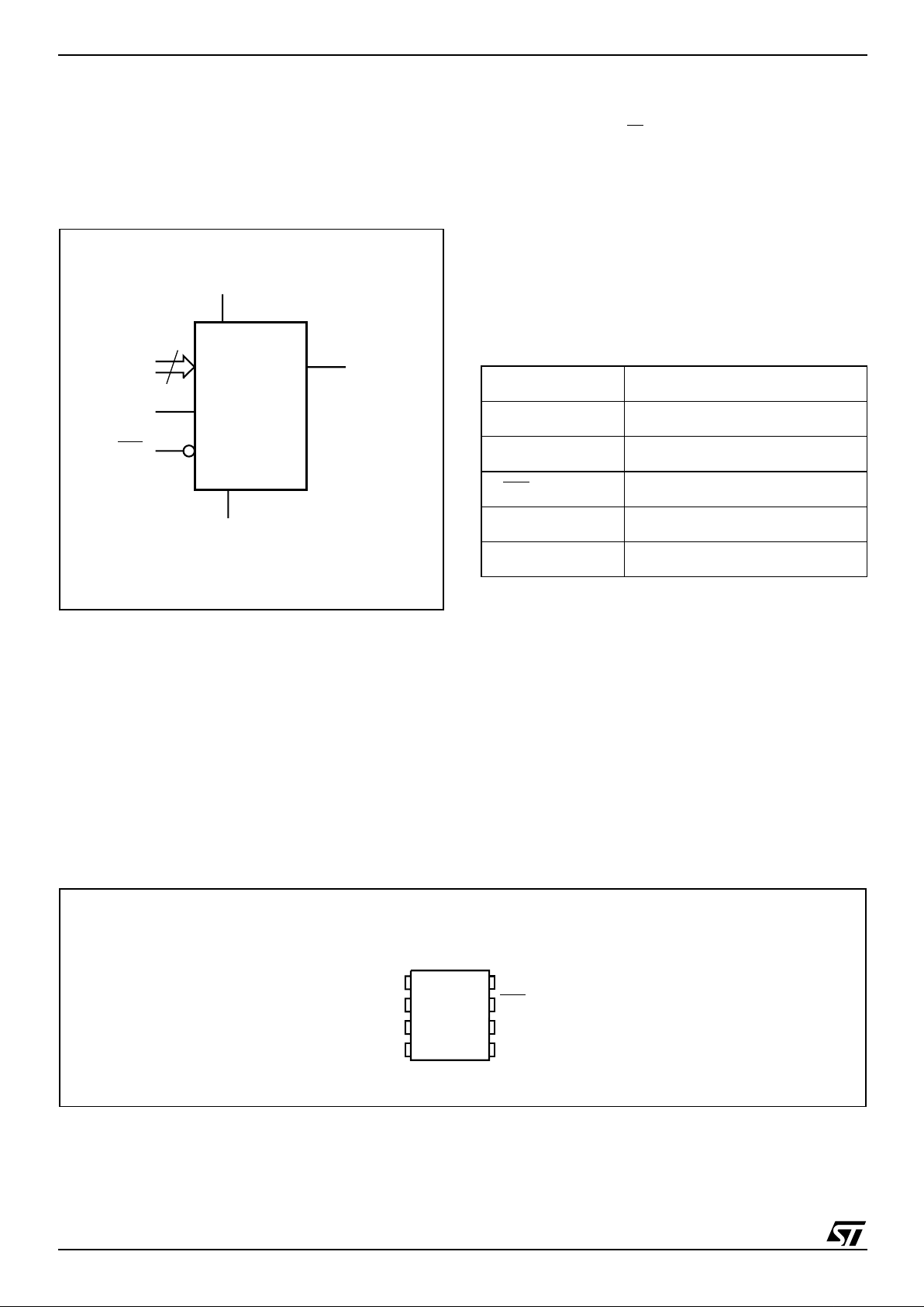
Figure 2. L o gi c Diag ram
These devices are compatible with the I
2
C memory protocol. This is a two wi re serial interface that
uses a bi-directional data bus and serial clock. The
devices carry a built-in 4-bit Device Type Identifier
code (1010) in accordance with the I
2
C bus defini-
tion.
The device behaves as a slave in the I
2
C protocol,
with all memory operations synchronized by the
serial clock. Read and Write operations are initiated by a Start condition, generated by the bus mas-
ter. The Start condition is followed by a Device
Select Code and RW
bit (as described in Table 2),
terminated by an acknowledge bit.
When writing data to the memory, the device in-
serts an acknowledge bit during the 9
th
bit time,
following the bus master’s 8-bit transmission.
When data is read by the bus master, the bus
master acknowledg es t he rec eipt of the data b yte
in the same way. Data transfers are terminated by
a Stop condition after an Ack for Write, and after a
NoAck for Read.
Table 1. Signal Names
Power On Reset: V
CC
Lock-Out Write Protect
In order to prevent data corruption and inadvertent
Write operations during Power-up, a Power On
Reset (POR) circuit is included. The internal reset
is held active until V
CC
has reached the POR
threshold value, and all operations are disabled –
the device will not respond to any command. In the
same way, when V
CC
drops from the operating
voltage, below the POR threshold value , all operations are disabled and the device will not respond
to any command. A stable and valid V
CC
must be
applied before applying any logic signal.
Figure 3. DIP, SO and TSSOP Connections
Note: 1. NC = Not Connected
2. See page 20 (onwards) f or package di m ensions , an d how to identify pin-1.
AI02033
3
E0-E2 SDA
V
CC
M24Cxx
WC
SCL
V
SS
E0, E1, E2 Chip Enable
SDA Serial Data
SCL Serial Clock
WC
Write Control
V
CC
Supply Voltage
V
SS
Ground
SDAV
SS
SCL
WC
V
CC
/ E2
AI02034E
M24Cxx
1
2
3
4
8
7
6
5
/ E2/ E2/ E2NC
/ E1
/ E1/ E1/ NCNC
/ E0
/ E0/ NC/ NCNC
/1Kb
/2Kb/4Kb/8Kb16Kb
3/26
M24C16, M24C08, M24C04, M 24C02, M24C01
SIGNAL DESCRIPTION
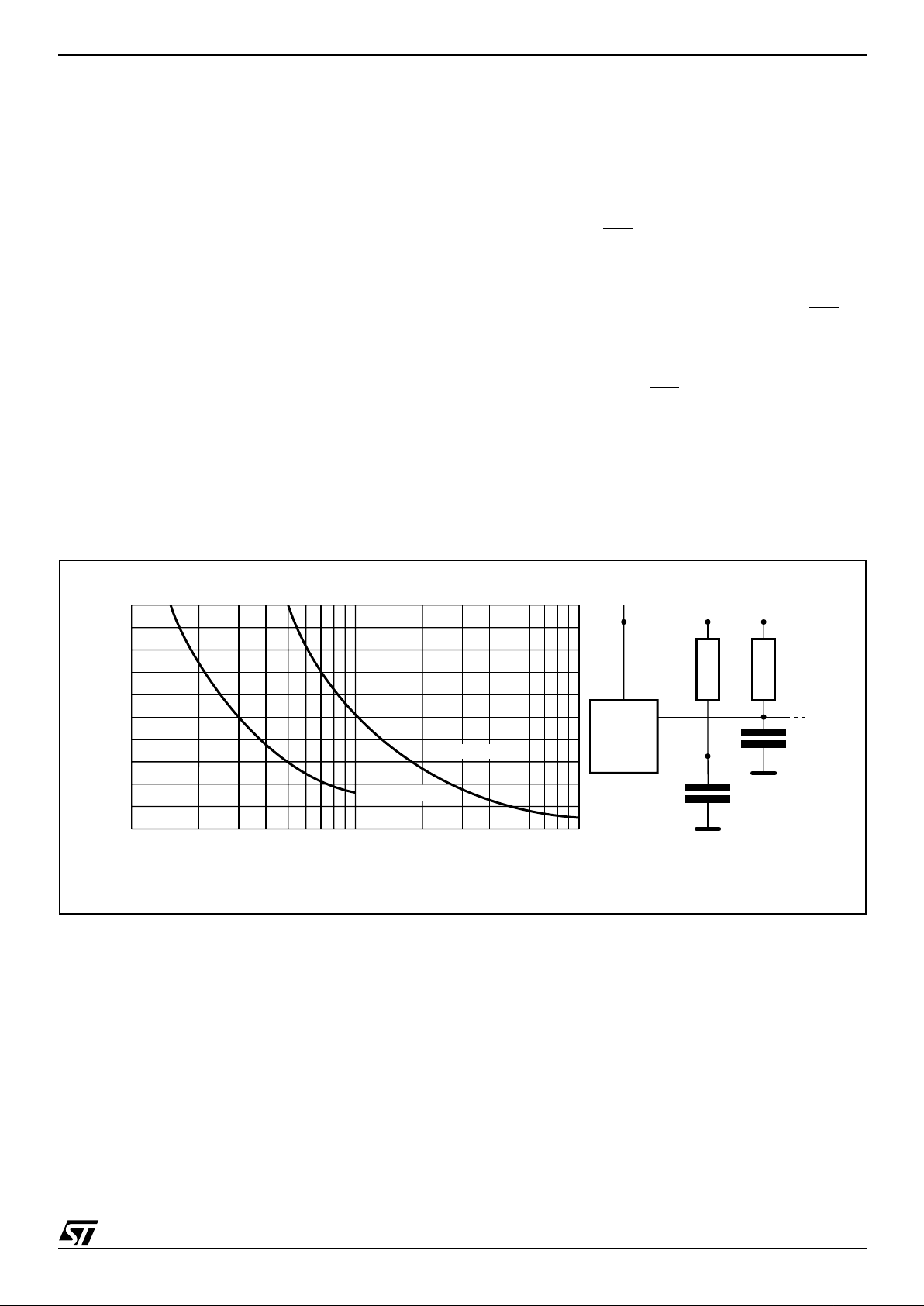
Serial Clock (SCL)
This input signal is u sed to strobe all data in and
out of the device. In applications where this signal
is used by slave devices to synchronize the bus to
a slower clock, the bus master must have an open
drain output, and a pull-up resistor can be connected from Serial Clock (SCL) to V
CC
. (Figure 4
indicates how the valu e of the pull-up resist or can
be calculated). In most applications , though, this
method of synchronization is no t employed, and
so the pull-up resistor is not necessary, provided
that the bus maste r has a push-pull (rather than
open drain) output.
Serial Data (SDA)
This bi-directional signal is used to transfer data in
or out of the device. It is an open drain output that
may be wire-OR’ed with ot her op en drai n or open
collector signals on the bus. A pull up resistor must
be connected from Serial Data (SDA) to V
CC
. (Figure 4 indicates how the value of the pull-up resistor
can be calculated).
Chip Enable (E0, E1, E2)
These input signals are used to set the value that
is to be looked for on the three least significant bits
(b3, b2, b1) of the 7-bit Device Select Code. These
inputs must be tied to V
CC
or VSS, to establish the
Device Select Code.
Write Control (WC
)
This input signal is useful for protecting the entire
contents of the memory from inadvertent write operations. Write operations are disabled to the entire memory array when Write Control (WC
) is
driven High. When unconnected, the signal is internally read as V
IL
, and Write operations are al-
lowed.
When Write Control (WC
) is driven High, Device
Select and Address bytes are acknowledged,
Data bytes are not acknowledged.
Figure 4. Maximum R
L
Value versus Bus Capacitance (C
BUS
) for an I2C Bus
AI01665
V
CC
C
BUS
SDA
R
L
MASTER
R
L
SCL
C
BUS
100
0
4
8
12
16
20
C
BUS
(pF)
Maximum RP value (kΩ)
10 1000
fc = 400kHz
fc = 100kHz
M24C16, M24C08, M24C04, M24C02, M24C01
4/26
Figure 5. I2C Bus Protocol
Table 2. Device Select Code
Note: 1. The mos t si gnificant bit, b7, is sent first .
2. E0, E1 and E2 are compared against the respe ct i ve external pins on th e m em ory devi ce.
3. A10, A9 and A8 repres ent most signif i cant bits of th e address.
Device Type Identifier
1
Chip Enable
2,3
RW
b7
b6 b5 b4 b3 b2 b1 b0
M24C01 Select Code 1010E2E1E0RW
M24C02 Select Code 1010E2E1E0RW
M24C04 Select Code 1010E2E1A8RW
M24C08 Select Code 1010E2A9A8RW
M24C16 Select Code 1010A10A9A8RW
SCL
SDA
SCL
SDA
SDA
START
Condition
SDA
Input
SDA
Change
AI00792B
STOP
Condition
1 23 789
MSB
ACK
START
Condition
SCL
1 23 789
MSB ACK
STOP
Condition
5/26
M24C16, M24C08, M24C04, M 24C02, M24C01
DEVICE OPERATION
The device supports the I
2
C proto col. This is summarized in Figure 5. Any device that sends data on
to the bus is defined to be a transmi tter, and any
device that reads the data to be a receiver. The
device that controls the data trans fer is known as
the bus master, and the other as the slave device.
A data transfer can only be initiated by the bus
master , w hic h w ill also provide t he s er ial cloc k f or
synchronization. The M24Cxx device is always a
slave in all communication.
Start Condition
Start is identified by a falling edge of Serial Data
(SDA) while Serial Clock (SCL) is stable in the
High state. A Start condition must precede any
data transfer command. The dev ice continuously
monitors (except during a Write cycle) Serial Data
(SDA) and Serial Clock (SCL) for a Start condition,
and will not respond unless one is given.
Stop Condition
Stop is identified by a rising edg e of Serial Data
(SDA) while Serial Clock (SCL) is stable and driven High. A Stop condition terminates communication between the device and the bus master. A
Read command that is followed by NoAck can be
followed by a Stop condition to force the device
into the Stand-by mode. A Stop condition at the
end of a Write command triggers th e internal EEPROM W r ite cycle.
Acknowledge Bit (ACK)
The acknowledge bit is used to indicate a successful byte transfer. The bus transmitter, whether it be
bus master or slave device, releases Serial Data
(SDA) after sending eight bits of data. During the
9
th
clock pulse period, the receiver pulls Serial
Data (SDA) Low to acknowledge the receipt of the
eight data bits.
Data Input
During data input, the device samples Serial Data
(SDA) on the rising edge of Serial Clock (SCL).
For correct device operation, Serial Data (SDA)
must be stable during the rising edge of Serial
Clock (SCL), and the Serial Data (SDA) signal
must change
only
when Serial Clock (SCL) is driv-
en Low.
Memory Addressing
To start communication be tween the bus master
and the slave device, the bus m aste r must initiate
a Start condition. Following this, the bus master
sends the Device Select Code, shown i n Table 2
(on Serial Data (SDA), most significant bit first).
The Device Select Code consists of a 4-bit Device
Type Identifier, and a 3-bit Chip Enable “Address”
(E2, E1, E0). To address the memory array, the 4bit Device Type Identifier is 1010b.
When the Device Select Code is received on Serial Data (SDA), the device only responds if the Chip
Enable Address is the same as the value on the
Chip Enable (E0, E1, E2) inputs.
The 8
th
bit is the Read/Write bit (RW). This bit is
set to 1 for Read and 0 for Write operations.
If a match occurs on the Device Select code , the
corresponding device gives an acknowledgment
on Serial Data (SDA) during the 9
th
bit time. If the
device does not match the Device Select code, it
deselects itself from the bus, and goes into Standby mode.
Devices with larger memory capacities (the
M24C16, M24C08 and M24C04) need more address bits. E0 i s not available f or use on dev ices
that need to use address line A8; E1 is not available for devices that need to use addres s line A9,
and E2 is not available for devices that need to use
address line A10 (see Figure 3 and Table 2 for details). Using the E0, E1 and E2 inputs pins, up to
eight M24C02 (or M24C01), four M24C04, two
M24C08 or one M24C16 device can be connected
to one I
2
C bus. In each case, and in the hybrid cases, this gives a total memory capacity of 16 Kbits,
2 KBytes (except where M24C01 devices are
used).
Table 3. Operating Modes
Note: 1. X = V
IH
or V
IL
.
Mode RW bit
WC
1
Bytes Initial Sequence
Current Address Read 1 X 1 START, Device Select, RW
= 1
Random Address Read
0X
1
START, Device Select, RW
= 0, Address
1 X reSTART, Device Select, RW
= 1
Sequential Read 1 X
≥
1 Similar to Current or Random Address Read
Byte Write 0
V
IL
1 START, Device Select, RW = 0
Page Write 0
V
IL
≤
16 START, Device Select, RW
= 0
M24C16, M24C08, M24C04, M24C02, M24C01
6/26
Figure 6. Wri t e Mo de S equences with WC=1 (data write inhibi ted)
Write Operations
Following a Start condition the bus master s ends
a Device Select Code with the RW
bit rese t to 0.
The device acknowledges this, as shown in Figure
7, and waits for an address byte. The device responds to the address byte with an ack nowledge
bit, and then waits for the data byte.
When the bus master generate s a Stop c ondition
immediately after the Ack bi t (in the “10
th
bit” time
slot), either at the end of a Byte Write or a Page
Write, the internal memory Write cycle is triggered.
A Stop condition at any other time slot does not
trigger the internal Write cycle.
During the internal Write cycle, Seria l Data (SDA)
and Serial Clock (SCL) are ignored, and t he device does not respond to any requests.
Byte Write
After the Device Select code and the address byte,
the bus master sends one data byte. If the addressed location is Write-protected, by Write Control (WC
) being driven High (during the period from
the Start condition until the end of the address
byte), the device replies to the data byte with
NoAck, as shown in Figure 6, and the location is
not modified. If, instead, the addressed location is
not Write-protected, the device replies with Ack.
The bus master terminates the transf er by generating a Stop condition, as shown in Figure 7.
Page Write
The Page Write mode allows u p to 16 byt es to be
written in a single Write cycle, provided that they
are all located in the same page in the memory:
that is, the most significant memory address bits
are the same. If more bytes are sent than will fit up
to the end of t he pa ge, a condition known as ‘ rollover’ occurs. This should be avoided, as data
starts to become overwritten in an implementation
dependent way.
The bus master s ends f rom 1 to 16 bytes of data,
each of which is acknowledged by the device if
Write Control (WC
) is Low. If the addressed loca-
tion is Write-protected, by Write Control (WC
) be-
ing driven High (during the period from the S tart
STOP
START
Byte Write DEV SEL BYTE ADDR DATA IN
WC
START
Page Write DEV SEL BYTE ADDR DATA IN 1 DATA IN 2
WC
DATA IN 3
AI02803C
Page Write
(cont'd)
WC (cont'd)
STOP
DATA IN N
ACK ACK NO ACK
R/W
ACK ACK NO ACK NO ACK
R/W
NO ACK NO ACK
7/26
M24C16, M24C08, M24C04, M 24C02, M24C01
condition until the end of the address byte), the device replies to the data bytes with NoAck, as
shown in Figure 6, and the locations are not modified. After each byte is transferred, the internal
byte address counter (the 4 least significant address bits only) is incremented. The transfer i s t erminated by the bus master generating a Stop
condition.
Figure 7. Wri t e Mo de S equences with W
C=0 (data write enabled)
STOP
START
BYTE WRITE DEV SEL BYTE ADDR DATA IN
WC
START
PAGE WRITE DEV SEL BYTE ADDR DATA IN 1 DATA IN 2
WC
DATA IN 3
AI02804B
PAGE WRITE
(cont'd)
WC (cont'd)
STOP
DATA IN N
ACK
R/W
ACK ACK
ACK ACK ACK ACK
R/W
ACKACK
M24C16, M24C08, M24C04, M24C02, M24C01
8/26
Figure 8. Wri t e C yc le Polling Flowc ha rt us i n g A C K
Minimizing System Delays by Polling On ACK
During the internal Write cycle, the device disconnects itself from the bus, and writes a copy of the
data from its internal latches to the memo ry cells.
The maximum Write time (t
w
) is shown in T ables
19 to 21, bu t the typical time is shorter. To m ake
use of this, a polling sequence can be used by the
bus master.
The sequence, as shown in Figure 8, is:
– Initial condition: a Write cycle is in progress.
– Step 1: the bus ma ster issues a Start condition
followed by a Device Select Code (the first byte
of the new instruction).
– Step 2: if the device is busy with the internal
Write cycle, no Ack will be returned and the bus
master goes back to Step 1. If the device has
terminated the internal Write cycle, it responds
with an Ack, indicating that the device is ready
to receive the second part of the instruction (the
first byte of this instruction having been sent
during Step 1).
WRITE Cycle
in Progress
AI01847C
Next
Operation is
Addressing the
Memory
START Condition
DEVICE SELECT
with RW = 0
ACK
Returned
YES
NO
YESNO
ReSTART
STOP
DATA for the
WRITE Operation
DEVICE SELECT
with RW = 1
Send Address
and Receive ACK
First byte of instruction
with RW = 0 already
decoded by the device
YESNO
START
Condition
Continue the
WRITE Operation
Continue the
Random READ Operation

9/26
M24C16, M24C08, M24C04, M 24C02, M24C01
Figure 9. Read Mode Sequences
Note: 1. The sev en most significan t bits of the Device Sele ct Code of a Random Read (in the 1st and 3rd bytes) m ust be identical.
Read Operations
Read operations are performed independently of
the state of the Write Control (WC
) signal.
Random Address Read
A dummy Write is performed to load the address
into the address counter (as shown in Figure 9) but
without
sending a Stop condition. Then, the bus
master sends another Start condition, and repeats
the Device Select Code, with the RW
bit set to 1.
The device acknowledges this, and outputs the
contents of the address ed byte. The bus master
must
not
acknowledge the byte, and terminates
the transfer with a Stop condition.
Current Address Read
The device has an internal address counter which
is incremented each time a byte is read. For the
Current Address Read operation, following a Start
condition, the bus master only sends a Device Select Code with the RW
bit set to 1. The device acknowledges this, an d o utputs the by te addres sed
by the internal address counter. The counter is
then incremented. T he bus master t erm inates t he
transfer with a Stop condition , as shown i n Figure
9,
without
acknowledging the byte.
Sequent i al Re ad
This operation can be used after a Current Address Read or a Random Address Read. The bus
START
DEV SEL * BYTE ADDR
START
DEV SEL DATA OUT 1
AI01942
DATA OUT N
STOP
START
CURRENT
ADDRESS
READ
DEV SEL DATA OUT
RANDOM
ADDRESS
READ
STOP
START
DEV SEL * DATA OUT
SEQUENTIAL
CURRENT
READ
STOP
DATA OUT N
START
DEV SEL * BYTE ADDR
SEQUENTIAL
RANDOM
READ
START
DEV SEL * DATA OUT 1
STOP
ACK
R/W
NO ACK
ACK
R/W
ACK ACK
R/W
ACK ACK ACK NO ACK
R/W
NO ACK
ACK ACK
R/W
ACK ACK
R/W
ACK NO ACK

M24C16, M24C08, M24C04, M24C02, M24C01
10/26
master
does
acknowledge the data byte output,
and sends additional clock pulses so that the device continues to output the next byte in sequence.
To terminate the stream of bytes, the bus master
must
not
acknowledge the last byte, and
must
generate a Stop condition, as shown in Figure 9.
The output data comes from consecutive address-
es, with the internal address counter automatically
incremented after each byte output. After the last
memory address, the address counter ‘rolls-over’,
and the device continues to output data from
memory address 00h.
Acknowledge in Read Mode
For all Read commands, the device waits, after
each byte read, for an acknowledgment during the
9
th
bit time. If the bus master does not drive Serial
Data (SDA) Low during this time, the device terminates the data transfer an d switches to its Standby mode.
INITIAL DELIVERY STATE
The device is delivered with the memory array
erased: all bits are set to 1 (each byte contains
FFh).

11/26
M24C16, M24C08, M24C04, M 24C02, M24C01
MAXIMUM R A TI N G
Stressing the de vice above the rating l isted in t he
Absolute Maximum Ratings" table may cause permanent damage to the dev ice. These are stress
ratings only and operation of the device at t hese or
any other conditions ab ove thos e indicated i n the
Operating sections of this spec ification is not im-
plied. Exposure to Absolute Maximum Rating conditions for extended periods may affect device
reliability. Refer also to the STMicroelectronics
SURE Program and other relevant quality documents.
Table 4. Absolute Maximum Ratings
Note: 1. IPC/JEDEC J-STD-020 A
2. JEDEC Std J E SD22-A114A (C1=1 00 pF, R1 =1500 Ω, R2=500 Ω)
Symbol Parameter Min. Max. Unit
T
STG
Storage Temperature –65 150 °C
T
LEAD
Lead Temperature during
Soldering
PDIP: 10 seconds
SO: 20 seconds (max)
1
TSSOP: 20 seconds (max)
1
260
235
235
°C
V
IO
Input or Output range –0.6 6.5 V
V
CC
Supply Voltage –0.3 6.5 V
V
ESD
Electrostatic Discharge Voltage (Human Body model)
2
–4000 4000 V

M24C16, M24C08, M24C04, M24C02, M24C01
12/26
DC AND AC PARAMETERS
This section summarizes t he operating and measurement conditions, and the DC and AC characteristics of the device. The parameters i n the DC
and AC Characteristic tables that follow are derived from tests performed under the Measure-
ment Conditions summarized in the relevant
tables. Designers should c heck that the o perat ing
conditions in their circuit match the m easurement
conditions when relying on the quoted parameters.
Table 5. Operating Conditions (M24Cxx-xx6)
Table 6. Operating Conditions (M24Cxx-xx3)
Table 7. Operating Conditions (M24Cxx-Wxx6)
Table 8. Operating Conditions (M24Cxx-Wxx3 )
Table 9. Operating Conditions (M24Cxx-Lxx6)
Table 10. Operating Conditions (M24Cxx-Rxx6)
Symbol Parameter Min. Max. Unit
V
CC
Supply Voltage 4.5 5.5 V
T
A
Ambient Operating Temperature –40 8 5 °C
Symbol Parameter Min. Max. Unit
V
CC
Supply Voltage 4.5 5.5 V
T
A
Ambient Operating Temperature –40 125 ° C
Symbol Parameter Min. Max. Unit
V
CC
Supply Voltage 2.5 5.5 V
T
A
Ambient Operating Temperature –40 8 5 °C
Symbol Parameter Min. Max. Unit
V
CC
Supply Voltage 2.5 5.5 V
T
A
Ambient Operating Temperature –40 125 ° C
Symbol Parameter Min. Max. Unit
V
CC
Supply Voltage 2.2 5.5 V
T
A
Ambient Operating Temperature –40 8 5 °C
Symbol Parameter Min. Max. Unit
V
CC
Supply Voltage 1.8 5.5 V
T
A
Ambient Operating Temperature –40 8 5 °C

13/26
M24C16, M24C08, M24C04, M 24C02, M24C01
Table 11. AC Measurement Conditions
Figure 10. AC Measurement I/O Waveform
Table 12. Input Parameters
Note: 1. TA = 25 °C, f = 400 kHz
2. Sampled only, not 100% tested.
Symbol Parameter Min. Max. Unit
C
L
Load Capacitance 100 pF
Input Rise and Fall Times 50 ns
Input Levels
0.2V
CC
to 0.8V
CC
V
Input and Output Timing Reference Levels
0.3V
CC
to 0.7V
CC
V
Symbol
Parameter
1,2
Test Condition Min. Max. Unit
C
IN
Input Capacitanc e (SDA) 8 pF
C
IN
Input Capacitance (other pins) 6 pF
Z
WCL
WC Input Impedance VIN < 0.5 V 5 70 k
Ω
Z
WCH
WC Input Impedance
V
IN
> 0.7V
CC
500 k
Ω
t
NS
Pulse width ignored
(Input Filter on SCL and SDA)
Single glitch 100 ns
AI00825B
0.8V
CC
0.2V
CC
0.7V
CC
0.3V
CC
Input and Output
Timing Reference Levels
Input Levels

M24C16, M24C08, M24C04, M24C02, M24C01
14/26
Table 13. DC Characteristics (M24Cxx-xx6)
Table 14. DC Characteristics (M24Cxx-xx3)
Symbol Parameter
Test Condition
(in addition to those in Table 5)
Min. Max. Unit
I
LI
Input Leakage Current
(SCL, SDA)
V
IN
= VSS or V
CC
± 2 µA
I
LO
Output Leakage Current V
OUT
= VSS or V
CC,
SDA in Hi-Z ± 2 µA
I
CC
Supply Current
V
CC
=5V, fc=400kHz (rise/fall time < 30ns)
2mA
I
CC1
Stand-by Supply Current
V
IN
= VSS or V
CC
, V
CC
= 5 V
1µA
V
IL
Input Low Voltage
(E2, E1, E0, SCL, SDA)
–0.3 0.3V
CC
V
Input Low Voltage (WC
) –0.3 0.5 V
V
IH
Input High Voltage
(E2, E1, E0, SCL, SDA, WC
)
0.7V
CC
VCC+1
V
V
OL
Output Low Voltage IOL = 3 mA, VCC = 5 V 0.4 V
Symbol Parameter
Test Condition
(in addition to those in Table 6)
Min. Max.
Unit
I
LI
Input Leakage Current
(SCL, SDA)
V
IN
= VSS or V
CC
± 2 µA
I
LO
Output Leakage Current V
OUT
= VSS or V
CC,
SDA in Hi-Z ± 2 µA
I
CC
Supply Current
V
CC
=5V, fc=400kHz (rise/fall time < 30ns)
3mA
I
CC1
Stand-by Supply Current
V
IN
= VSS or V
CC
, V
CC
= 5 V
5µA
V
IL
Input Low Voltage
(E2, E1, E0, SCL, SDA)
–0.3 0.3V
CC
V
Input Low Voltage (WC
) –0.3 0.5 V
V
IH
Input High Voltage
(E2, E1, E0, SCL, SDA, WC
)
0.7V
CC
VCC+1
V
V
OL
Output Low Voltage IOL = 3 mA, VCC = 5 V 0.4 V

15/26
M24C16, M24C08, M24C04, M 24C02, M24C01
Table 15. DC Characteristics (M24Cxx-Wxx6)
Table 16. DC Characteristics (M24Cxx-Wxx3)
Note: 1. This is preliminary data.
Symbol Parameter
Test Condition
(in addition to those in Table 7)
Min.
Max. Unit
I
LI
Input Leakage Current
(SCL, SDA)
V
IN
= VSS or V
CC
± 2 µA
I
LO
Output Leakage Current V
OUT
= VSS or V
CC,
SDA in Hi-Z ± 2 µA
I
CC
Supply Current
V
CC
=2.5V , fc=400kHz (rise/fall time < 30ns)
1mA
I
CC1
Stand-by Supply Current
V
IN
= VSS or V
CC
, V
CC
= 2.5 V
0.5 µA
V
IL
Input Low Voltage
(E2, E1, E0, SCL, SDA)
–0.3 0.3V
CC
V
Input Low Voltage (WC
) –0.3 0.5 V
V
IH
Input High Voltage
(E2, E1, E0, SCL, SDA, WC
)
0.7V
CC
VCC+1
V
V
OL
Output Low Voltage IOL = 2.1 mA, VCC = 2.5 V 0.4 V
Symbol Parameter
Test Condition
(in addition to those in Table 8)
Min.
1
Max.
1
Unit
I
LI
Input Leakage Current
(SCL, SDA)
V
IN
= VSS or V
CC
± 2 µA
I
LO
Output Leakage Current V
OUT
= VSS or V
CC,
SDA in Hi-Z ± 2 µA
I
CC
Supply Current
V
CC
=2.5V , fc=400kHz (rise/fall time < 30ns)
3mA
I
CC1
Stand-by Supply Current
V
IN
= VSS or V
CC
, V
CC
= 2.5 V
2µA
V
IL
Input Low Voltage
(E2, E1, E0, SCL, SDA)
–0.3 0.3V
CC
V
Input Low Voltage (WC
) –0.3 0.5 V
V
IH
Input High Voltage
(E2, E1, E0, SCL, SDA, WC
)
0.7V
CC
VCC+1
V
V
OL
Output Low Voltage IOL = 2.1 mA, VCC = 2.5 V 0.4 V
M24C16, M24C08, M24C04, M24C02, M24C01
16/26
Table 17. DC Characteristics (M24Cxx-Lxx6)
Table 18. DC Characteristics (M24Cxx-Rxx6)
Symbol Parameter
Test Condition
(in addition to those in Table 9)
Min.
Max. Unit
I
LI
Input Leakage Current
(SCL, SDA)
V
IN
= VSS or V
CC
± 2 µA
I
LO
Output Leakage Current V
OUT
= VSS or V
CC,
SDA in Hi-Z ± 2 µA
I
CC
Supply Current
V
CC
=2.5V , fc=400kHz (rise/fall time < 30ns)
1mA
I
CC1
Stand-by Supply Current
V
IN
= VSS or V
CC
, V
CC
= 2.5 V
0.5 µA
V
IL
Input Low Voltage
(E2, E1, E0, SCL, SDA)
–0.3 0.3V
CC
V
Input Low Voltage (WC
) –0.3 0.5 V
V
IH
Input High Voltage
(E2, E1, E0, SCL, SDA, WC
)
0.7V
CC
VCC+1
V
V
OL
Output Low Voltage IOL = 2.1 mA, VCC = 2.2 V 0.4 V
Symbol Parameter
Test Condition
(in addition to those in Table 10)
Min.
Max. Unit
I
LI
Input Leakage Curren t
(SCL, SDA)
V
IN
= VSS or V
CC
± 2 µA
I
LO
Output Leakage Current V
OUT
= VSS or V
CC,
SDA in Hi-Z ± 2 µA
I
CC
Supply Current
V
CC
=1.8V , fc=400kHz (rise/fall time < 30ns)
0.8
mA
I
CC1
Stand-by Supply Current V
IN
= VSS or V
CC
, V
CC
= 1.8 V
0.3
µA
V
IL
Input Low Voltage
(E2, E1, E0, SCL, SDA)
2.5 V ≤ V
CC
– 0.3
0.3 V
CC
V
1.8 V ≤ V
CC
< 2.5 V – 0.3
0.25 V
CC
V
Input Low Voltage (WC
) –0.3 0.5 V
V
IH
Input High Voltage
(E2, E1, E0, SCL, SDA, WC
)
0.7V
CC
VCC+1 V
V
OL
Output Low Voltage IOL = 0.7 mA, VCC = 1.8 V
0.2
V
17/26
M24C16, M24C08, M24C04, M 24C02, M24C01
Table 19. AC Characteristics (M24Cxx-xx6, M24Cx x-Wxx3)
Note: 1. For a reSTART condition, or followi ng a Write cycle.
2. Sampled only, not 100% tested.
3. To avoid spurious START and STOP conditions, a minimum delay is placed between SCL=1 and the falling or rising edge of SDA.
4. This is preliminary data for M24Cxx-Wxx3.
Table 20. AC Characteristics (M24Cxx-xx3, M24Cxx-Wxx6, M24Cxx-Lxx6)
Note: 1. For a reSTART condition, or followi ng a Write cycle.
2. Sampled only, not 100% tested.
3. To avoid spurious START and STOP conditions, a minimum delay is placed between SCL=1 and the falling or rising edge of SDA.
4. 10ms write time is offered on the standard device. 5ms write time is offered on new products bearing the Process Identification letter
“W” on the pa ck age, as desc ri bed in T able 23.
Test conditions specified in Table 11 and Table 5 or 8
Symbol Alt. Parameter
Min.
4
Max.
4
Unit
f
C
f
SCL
Clock Frequency 400 kHz
t
CHCL
t
HIGH
Clock Pulse Width High 600 ns
t
CLCH
t
LOW
Clock Pulse Width Low 1300 ns
t
DL1DL2
2
t
F
SDA Fall Time 20 300 ns
t
DXCX
t
SU:DAT
Data In Set Up Time 100 ns
t
CLDX
t
HD:DAT
Data In Hold Time 0 ns
t
CLQX
t
DH
Data Out Hold Time 200 ns
t
CLQV
3
t
AA
Clock Low to Next Data Valid (Access Time) 200 900 ns
t
CHDX
1
t
SU:STA
Start Condition Set Up Time 600 ns
t
DLCL
t
HD:STA
Start Condition Hold Time 600 ns
t
CHDH
t
SU:STO
Stop Condition Set Up Time 600 ns
t
DHDL
t
BUF
Time between Stop Condition and Next Start Condition 1300 ns
t
W
t
WR
Write Time 5 ms
Test conditions specified in Table 11 and Table 6 or 7 or 9
Symbol Alt. Parameter
Min. Max.
Unit
f
C
f
SCL
Clock Frequency 400 kHz
t
CHCL
t
HIGH
Clock Pulse Width High 600 ns
t
CLCH
t
LOW
Clock Pulse Width Low 1300 ns
t
DL1DL2
2
t
F
SDA Fall Time 20 300 ns
t
DXCX
t
SU:DAT
Data In Set Up Time 100 ns
t
CLDX
t
HD:DAT
Data In Hold Time 0 ns
t
CLQX
t
DH
Data Out Hold Time 200 ns
t
CLQV
3
t
AA
Clock Low to Next Data Valid (Access Time) 200 900 ns
t
CHDX
1
t
SU:STA
Start Condition Set Up Time 600 ns
t
DLCL
t
HD:STA
Start Condition Hold Time 600 ns
t
CHDH
t
SU:STO
Stop Condition Set Up Time 600 ns
t
DHDL
t
BUF
Time between Stop Condition and Next Start Condition 1300 ns
t
W
t
WR
Write Time
10 or
4
5
ms

M24C16, M24C08, M24C04, M24C02, M24C01
18/26
Table 21. AC Characteristics (M24Cxx-Rxx6)
Note: 1. For a reSTART condition, or followi ng a Write cycle.
2. Sampled only, not 100% tested.
3. To avoid spurious START and STOP conditions, a minimum delay is placed between SCL=1 and the falling or rising edge of SDA.
4. 100kHz clock frequency is offered on the standard device. 400kHz clock frequency is offered on new products bearing the Proce ss
Identifi cation letter “W” on the package, as described in Table 2 3.
Test conditions specified in Table 11 and Table 10
Symbol Alt. Parameter
Min. Max. Min.
4
Max.
4
Unit
f
C
f
SCL
Clock Frequency 100 400 kHz
t
CHCL
t
HIGH
Clock Pulse Width High 4000 600 ns
t
CLCH
t
LOW
Clock Pulse Width Low 4700 1300 ns
t
DL1DL2
2
t
F
SDA Fall Time 20 300 20 300 ns
t
DXCX
t
SU:DAT
Data In Set Up Time 250 100 ns
t
CLDX
t
HD:DAT
Data In Hold Time 0 0 ns
t
CLQX
t
DH
Data Out Hold Time 200 200 ns
t
CLQV
3
t
AA
Clock Low to Next Data Valid (Access
Time)
200 3500 200 900 ns
t
CHDX
1
t
SU:STA
Start Condition Set Up Time 4700 600 ns
t
DLCL
t
HD:STA
Start Condition Hold Time 4000 600 ns
t
CHDH
t
SU:STO
Stop Condition Set Up Time 4000 600 ns
t
DHDL
t
BUF
Time between Stop Condition and
Next Start Condition
4700 1300 ns
t
W
t
WR
Write Time 10 5 ms

19/26
M24C16, M24C08, M24C04, M 24C02, M24C01
Figure 11. AC Waveforms
SCL
SDA In
SCL
SDA Out
SCL
SDA In
tCHCL
tDLCL
tCHDX
START
Condition
tCLCH
tDXCXtCLDX
SDA
Input
SDA
Change
tCHDH tDHDL
STOP
Condition
Data Valid
tCLQV tCLQX
tCHDH
STOP
Condition
tCHDX
START
Condition
Write Cycle
tW
AI00795C
START
Condition
M24C16, M24C08, M24C04, M24C02, M24C01
20/26
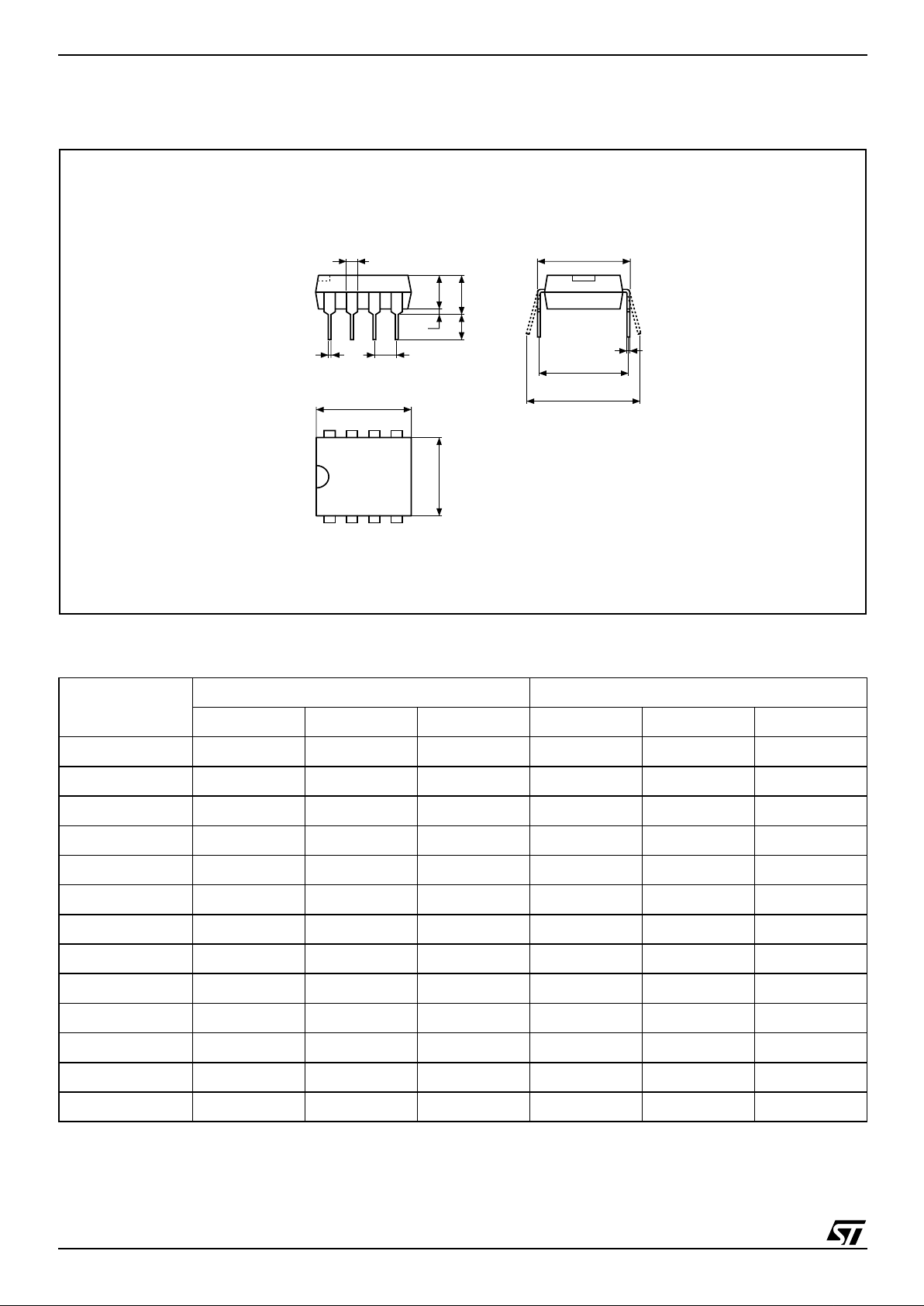
PACKAGE MECHANICAL
PDIP8 – 8 pin Plastic DIP, 0.25mm lead frame, Package Outline
Notes: 1. Drawing is not to scale.
PDIP8 – 8 pin Plastic DIP, 0.25mm lead frame, Package Mechanical Data
PDIP-B
A2
A1AL
be
D
E1
8
1
c
eA
b2
eB
E
Symb.
mm inches
Typ. Min. Max. T yp. Min. Max.
A 5.33 0.210
A1 0.38 0.015
A2 3.30 2.92 4.95 0.130 0.115 0.195
b 0.46 0.36 0.56 0.018 0.014 0.022
b2 1.52 1.14 1.78 0.060 0.045 0.070
c 0.25 0.20 0.36 0.010 0.008 0.014
D 9.27 9.02 10.16 0.365 0.355 0.400
E 7.87 7.62 8.26 0.310 0.300 0.325
E1 6.35 6.10 7.11 0.250 0.240 0.280
e 2.54 – – 0.100 – –
eA 7.62 – – 0.300 – –
eB 10.92 0.430
L 3.30 2.92 3.81 0.130 0.115 0.150
21/26
M24C16, M24C08, M24C04, M 24C02, M24C01
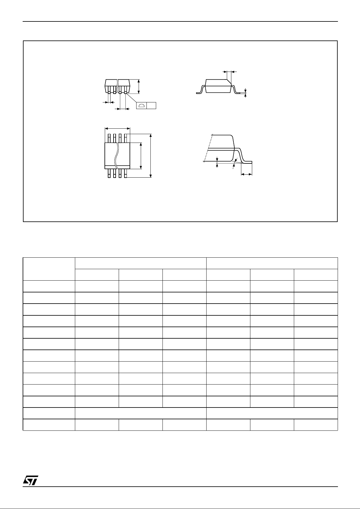
SO8 narrow – 8 lead Plastic Small Outline, 150 mils body width, Package Ou tline
Note: Drawing is not to scale.
SO8 narrow – 8 lead Plastic Small Outline, 150 mils body width, Package M echa ni cal Data
SO-a
E
N
CP
B
e
A
D
C
LA1 α
1
H
h x 45˚
Symb.
mm inches
Typ. Min. Max. Typ. Min. Max.
A 1.35 1.75 0.053 0.069
A1 0.10 0.25 0.004 0.010
B 0.33 0.51 0.013 0.020
C 0.19 0.25 0.007 0.010
D 4.80 5.00 0.189 0.197
E 3.80 4.00 0.150 0.157
e 1.27 – – 0.050 – –
H 5.80 6.20 0.228 0.244
h 0.25 0.50 0.010 0.020
L 0.40 0.90 0.016 0.035
α
0° 8° 0° 8°
N8 8
CP 0.10 0.004
M24C16, M24C08, M24C04, M24C02, M24C01
22/26
TSSOP8 – 8 lead Thin Shrink Small Outline, Package Outl ine
Notes: 1. Drawing is not to scale.
TSSOP8 – 8 lead Thin Shrink Small Outline, Package Mec han ical Data
TSSOP8AM
1
8
CP
c
L
EE1
D
A2A
α
eb
4
5
A1
L1
Symbol
mm inches
Typ. Min. Max. Typ. Min. Max.
A 1.200 0.0472
A1 0.050 0.150 0.0020 0.0059
A2 1.000 0.800 1. 050 0.0394 0.0315 0.0413
b 0.190 0.300 0.0075 0.0118
c 0.090 0.200 0.0035 0.0079
CP 0.100 0.0039
D 3.000 2.900 3.100 0.1181 0.1142 0.1220
e 0.650 – – 0.0256 – –
E 6.400 6.200 6. 600 0.2520 0.2441 0.2598
E1 4.400 4.300 4. 500 0.1732 0.1693 0.1772
L 0.600 0.450 0.750 0.0236 0.0177 0.0295
L1 1.000 0.0394
α
0° 8° 0° 8°

23/26
M24C16, M24C08, M24C04, M 24C02, M24C01
TSSOP8 3x3mm² – 8 lead Thin Shrink Sma ll Outline, 3x3mm² bo dy size, Packag e Outlin e
Notes: 1. Drawing is not to scale.
TSSOP8 3x3mm² – 8 lead Thin Shrink Small Outline, 3x3mm² body size, Package Mechanical Data
TSSOP8BM
1
8
CP
c
L
EE1
D
A2A
α
eb
4
5
A1
L1
Symbol
mm inches
Typ. Min. Max. T yp. Min. Max.
A 1.100 0.0433
A1 0.050 0.150 0.0020 0.0059
A2 0.850 0.750 0.950 0.0335 0.0295 0.0374
b 0.250 0.400 0.0098 0.0157
c 0.130 0.230 0.0051 0.0091
D 3.000 2.900 3.100 0.1181 0.1142 0.1220
E 4.900 4.650 5.150 0.1929 0.1831 0.2028
E1 3.000 2.900 3.100 0.1181 0.1142 0.1220
e 0.650 – – 0.0256 – –
CP 0.100 0.0039
L 0.550 0.400 0.700 0.0217 0.0157 0.0276
L1 0.950 0.0374
α
0° 6° 0° 6°

M24C16, M24C08, M24C04, M24C02, M24C01
24/26
PART NUMBERING
Table 22. Ordering Information Scheme
Note: 1. 2.5 to 5.5V device s beari ng th e pr oces s lett er “W” i n the p acka ge mar kin g (on th e top sid e of the pac kage , on th e righ t side, see
Table 23, below), guarantee a maximum write time of 5ms, instead of the standard 10ms. For more information about these devices,
and their device identification, please ask your ST Sales Office for Process Change Notices PCN MPG/EE/0061 and 0062
(PCEE0061 and PCE E 0062).
2. Used only f or M24Cxx -xx3
For a list of available options (speed, package,
etc.) or for further information on any aspect of this
device, please contact your neares t ST Sales O ffice.
Table 23. How to Identify Current and New Products by the Process Identification Letter
Note: 1. This example comes from the S0 8 package. Other packages have sim i l ar i nformati on. For furth er informat i on, pleas e ask your ST
Sales Offi ce for Process Change Notices PCN MPG/EE/0061 and 0062 (PCE E0061 and PC EE0062).
Example: M24C08 –WDW6T/W
Device Type
M24 = I
2
C serial access EEPROM
Device Function
16 = 16 Kbit (2048 x 8)
08 = 8 Kbit (1024 x 8)
04 = 4 Kbit (512 x 8)
02 = 2 Kbit (256 x 8)
01 = 1 Kbit (128 x 8)
Operating Voltage
blank = V
CC
= 4.5 to 5.5V (400kHz)
W
1
= VCC = 2.5 to 5.5V (400kHz)
L = V
CC
= 2.2 to 5.5V (400kHz)
R = V
CC
= 1.8 to 5.5V (400kHz)
Package
BN = PDIP8
MN = SO8 (150 mil width)
DW = TSSOP8 (169 mil width)
DS = TSSOP8 (3x3mm² body size, MSOP8)
Temperature Range
6 = –40 to 85 °C
3 = –40 to 125 °C
Option
T = Tape & Reel Packing
Process
2
blank = F6SP20%
/W = F6SP36%
Markings on Current Products
1
Markings on New Products
1
24CxxW6
ST xxxxL
24CxxW6
ST xxxxW
25/26
M24C16, M24C08, M24C04, M 24C02, M24C01
REVISION HISTORY
Table 24. Document Revision History
Date Rev. Description of Revision
10-Dec-1999 2.4
TSSOP8 Turned-Die package removed (p 2 and order information)
Lead temperature added for TSSOP8 in table 2
18-Apr-2000 2.5 Labelling change to Fig-2D, correction of values for ‘E’ and main caption for Tab-13
05-May-2000 2.6 Extra labelling to Fig-2D
23-Nov-2000 3.0
SBGA package information removed to an annex document
-R range changed to being the -S range, and the new -R range added
19-Feb-2001 3.1
SBGA package information put back in this document
Lead Soldering Temperature in the Absolute Maximum Ratings table amended
Write Cycle Polling Flow Chart using ACK illustration updated
References to PSDIP changed to PDIP and Package Mechanical data updated
Wording brought in to line with standard glossary
20-Apr-2001 3.2 Revision of DC and AC characteristics for the -S series
08-Oct-2001 3.3 Ball numbers added to the SBGA connections and package mechanical illustrations
09-Nov-2001 3.4 Specification of Test Condition for Leakage Currents in the DC Characteristics table improved
30-Jul-2002 3.5
Document reformatted using new template. SBGA5 package removed
TSSOP8 (3x3mm² body size) package (MSOP8) added. -L voltage range added
04-Feb-2003 3.6 Document title spelt out more fully. “W”-marked devices with tw=5ms added.
05-May-2003 3.7
-R voltage range upgraded to 400kHz working, and no longer preliminary data.
5V voltage range at temperature range 3 (-xx3) no longer preliminary data.
-S voltage range removed. -Wxx3 voltage+temp ranged added as preliminary data.

M24C16, M24C08, M24C04, M24C02, M24C01
26/26
Informa tion furnished is believed to be accurat e and reliabl e. However, STMicroelectroni cs assumes no responsib ility for the consequences
of use of such information nor for any infringement of patents or other rights of third parties which may result from its use. No license is granted
by implication or otherwi se under any patent or pat ent righ ts of STMic roelectronics. Specificat i ons ment i oned in th i s publication are subj ect
to change without notice. This publication supersedes and replaces all information previously supplied. STMicroelectronics products are not
authoriz ed for use as c ri tical components in li fe support devices or sy st ems without expre ss wri tten appr oval of STMicroelectronics.
The ST logo is regis tered trademark of STM i croelec tronics
All other names are the property of their r espective owners
© 2003 STMicroelectronics - All Rights Reserved
STMicroelectronics gro up of compan i es
Australia - Brazi l - Canada - Chin a - F i nl and - Franc e - Germany - Hong Kong -
India - Is rael - Italy - Japan - Malaysia - Mal t a - M orocco - Singapore - Spain - Sweden - Switz erland - United Kin gdom - United States.
www.st.com
 Loading...