M22101
M22102
4 X 4 X 2 CROSSPOINT SWITCHES
WITH CONTROLMEMORY
.LOW ON RESISTANCE– 75Ω TYPAT
VDD=12V
.”BUILT-IN” LATCHED INPUTS
.LARGE ANALOG SIGNALCAPACITY±V
DD
/2
.10 MHz SWITCH BANDWITH
.MATCHED SWITCHCHARACTERISTICS
.∆ RON = 8 Ω TYP, AT V
DD
=12V
.HIGH LINEARITY – 0.25 % DISTORTION TYP,
AT f = 1 kHz, VIN= 5 V, VDD-VSS= 10 V AND
RI = 1 Ω
.STANDARD CMOS NOISEIMMUNITY
DESCRIPTION
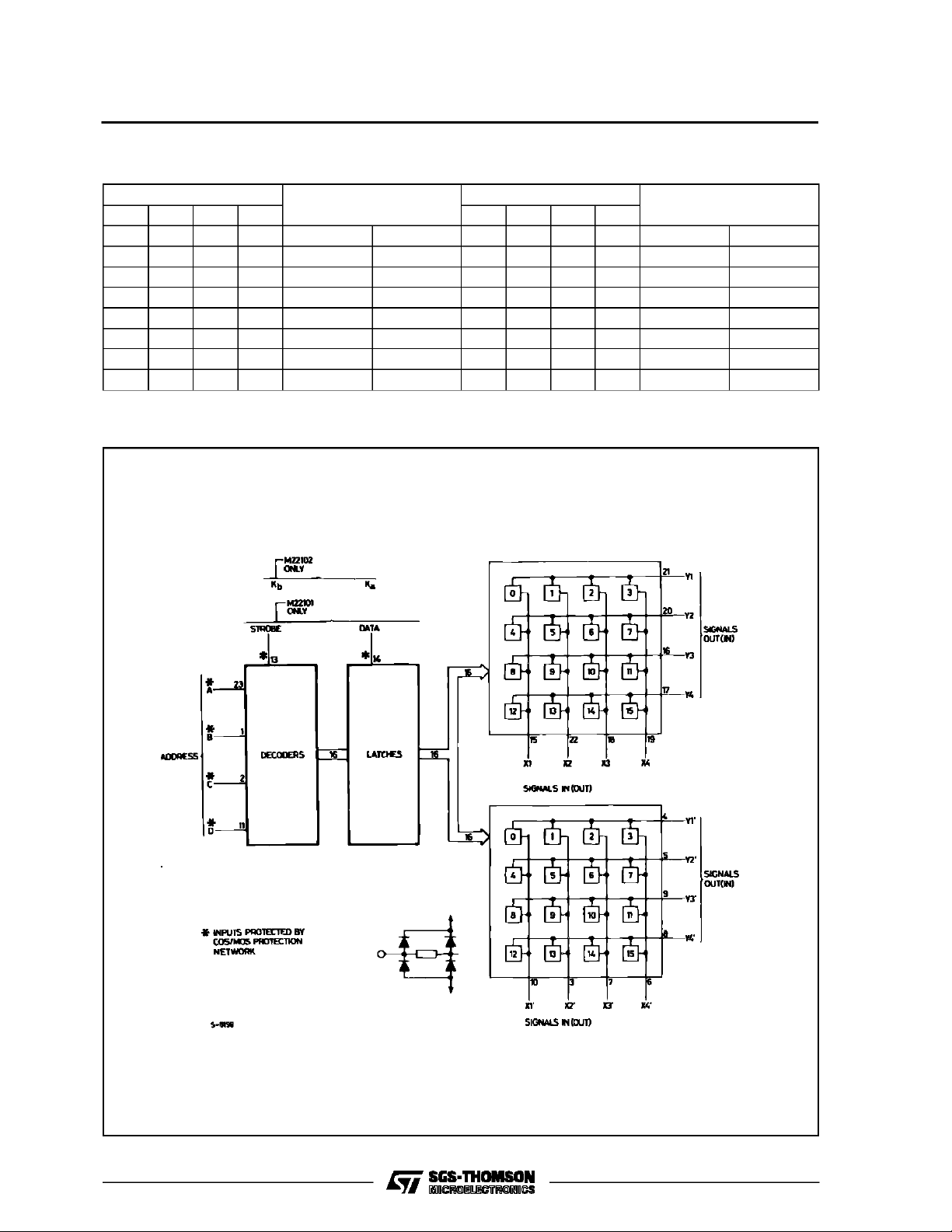
TheM22101 and M22102 crosspoint switches con-
sist of 4 x 4 x 2 arrays of crosspoints (transmission
gates), 4-line to 16-linedecoders, and 16 latchcircuits.Anyone ofthe sixteen crosspoint pairscan be
selected by applying the appropriate four-line addressandanynumber ofcrosspoint pairscanbeON
simultaneously. Corresponding crosspointsin each
arrayare turned on and OFFsimultaneously, also.
In the M22101, the selected crosspoint pair can be
turnedon oroff by applyingalogical ONEor ZERO,
respectively, to the data input,and applying aONE
to the strobe input. When the device is”power-up”,
the state of the16 switches is indeterminate.
Therefore all switches mustbe turned offby putting
the strobe hight,data-in-low, and theaddressing all
switches in succession.
The selected pair of crosspoints in the M22102 is
turnedon by applying a logical ONE to the Ka(set)
input whilealogical ZEROis on theKb(reset) input,
and turned off by applying a logical ONE to the K
input while a logical ZEROis on theKainput.In this
respectthecontrol latches oftheM22102 aresimilar
to SET/RESET flip-flops. They differ, however, in
thatthe simultaneousapplication of ONEstothe K
and Kbinputs turns off (resets) all crosspoints. All
crosspoints in both devices must be turned off as
VDDis applied.
B1
(PlasticPackage)
ORDER CODES :
M22XXX B1 M22XXX F1
(CeramicPackage)
F1
b
a
PIN CONNECTIONS
September 1988
1/8

M22101/M22102
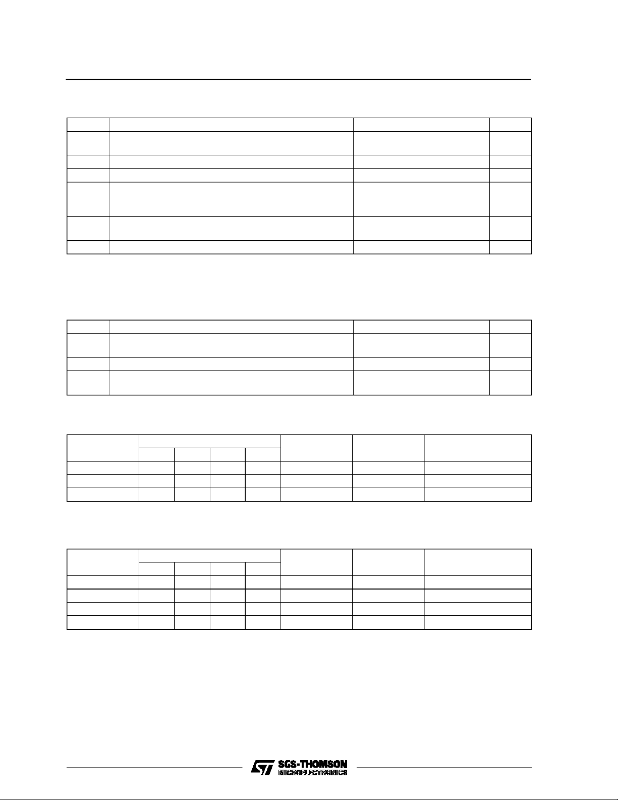
ABSOLU TE M AXIMU M R AT ING
Symbol Parameter Value Unit
V
DD
V
P
T
T
Stressesabove thoselistedunder ”Absolute Maximum Ratings”maycause permanent damagetothedevice. Thisisastressratingonlyand functional
operation ofthe device at these or any otherconditions above thoseindicatedintheoperational sections of thisspecification isnot implied.Exposure
to absolute maximumratingconditions forexternal periods mayaffect device reliability.
RECO MM ENDED OPERAT I N G CO NDI TIONS
Symbol Parameter Value Unit
V
V
T
Supply Voltage: Ceramic Type
Plastic Type
Input Voltage -0.5 to VDD+ 0.5 V
i
I
DC Input Current (any one input) ± 10 mA
I
Total Power Dissipation (per package)
tot
-0.5 to +20
-0.5 to +18
200
Dissipation per Output Transistor
for Top = Full Package Temperature Range
Operating Temperature: Ceramic Type
op
Plastic Type
Storage Temperature -65 to +150
stg
Supply Voltage: Ceramic Type
DD
Plastic Type
Input Voltage 0 to V
I
Operating Temperature: Ceramic Type
op
Plastic Type
100
-55 to +125
-40 to +85
3to18
3to15
DD
-55 to +125
-40 to +85
V
V
mW
mW
o
C
o
C
o
C
V
V
V
o
C
o
C
CONT RO L TRUT H TABLE FOR M22101
Function
ABCD
Switch-on 1 1 1 1 1 1 (X4 Y4) & (X4’ Y4’)
Switch-off 1 1 1 1 1 0 (X4 Y4) & (X4’ Y4’)
No Change X X X X 0 X XXXX
Note: 1=High,0 = Low, X= Don’tCare
Address
Strobe Data Select
CONT RO L TRUT H TABLE FOR M22102
Function
ABCD
Switch-on 1 1 1 1 1 0 (X4 Y4) & (X4’ Y4’)
Switch-off 1 1 1 1 0 1 (X4 Y4) & (X4’ Y4’)
All Switch-off X X X X 1 1 All
No Change X X X X 0 0 XXXX
Note: 1=High,0 = Low, X= Don’tCare
Address
Strobe Data Select
2/8

DECODER TRUTH TABLE
M22101/M22102
Address
ABCD ABCD
0000 X1Y1 X1’Y1’ 0001 X1Y3 X1’Y3’
1000 X2Y1 X2’Y1’ 1001 X2Y3 X2’Y3’
0100 X3Y1 X3’Y1’ 0101 X3Y3 X3’Y3’
1100 X4Y1 X4’Y1’ 1101 X4Y3 X4’Y3’
0010 X1Y2 X1’Y2’ 0011 X1Y4 X1’Y4’
1010 X2Y2 X2’Y2’ 1011 X2Y4 X2’Y4’
0110 X3Y2 X3’Y2’ 0111 X3Y4 X3’Y4’
1110 X4Y2 X4’Y2’ 1111 X4Y4 X4’Y4’
Select
Address
Select
FUNCTIONAL AND BLOCK DIAGRAM
3/8
 Loading...