

SGS Thomson Microelectronics M2201 Datasheet
2-Wires 1 Kbit (x8) Serial EEPROM
TWO WIRE SERIAL INTERFACE
100.000 ERASE/WRITE CYCLES with
100 YEARS DA TA RETENTION at 55°C
SINGLE SUPPLY VOLTAGE:
– 4.5V to 5.5V for M2201 version
– 2.7V to 5.5V for M2201V version
HARDWARE WRITE CONT ROL
100 KBIT TRANSFER RATE
BYTE WRITE
PAGE WRITE (up to 4 BYTES)
SELF TIMED PROGRAMMING CYCLE
AUTOMATIC ADDRESS INCREME NTING
ENHANCED ESD/LATCH UP
DESCRIPTION
The M2201 is a simplified 2-wire bus 1 Kbit electrically erasable programmable memory (EEPROM),
organized as 128 x8 bits. It is manufactured in
STMicroelectronics’s Hi-Endurance Advanced
CMOS technology which guarantees a data retention of 100 years at 55°C.
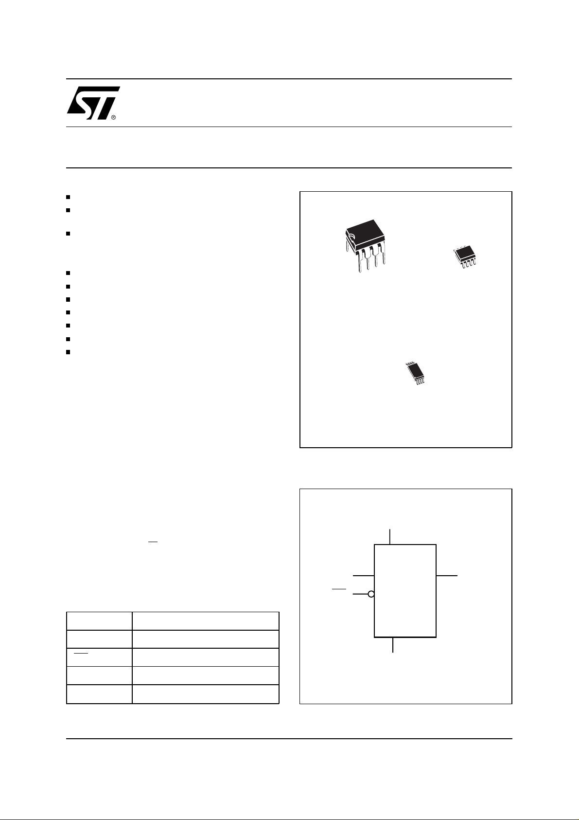
The M2201 is available in Plastic Dual-in-Line,
Plastic Small Outline and Thin Shrink Small Outline packages.
The memory is compatible with a two wire serial
interface which uses a bi-directional data bus and
serial clock. Read and write operations are initiated by a START condition generated by the bus
master and ended by a STOP condition.
Address bits and R
byte, instead of two (or three) bytes for the standard
2
C protocol.
I
T ab le 1. Signal Names
W bit are defined in one single
8
1
PSDIP8 (B)
0.25mm Frame
8
TSSOP8 (DW)
169 mil width
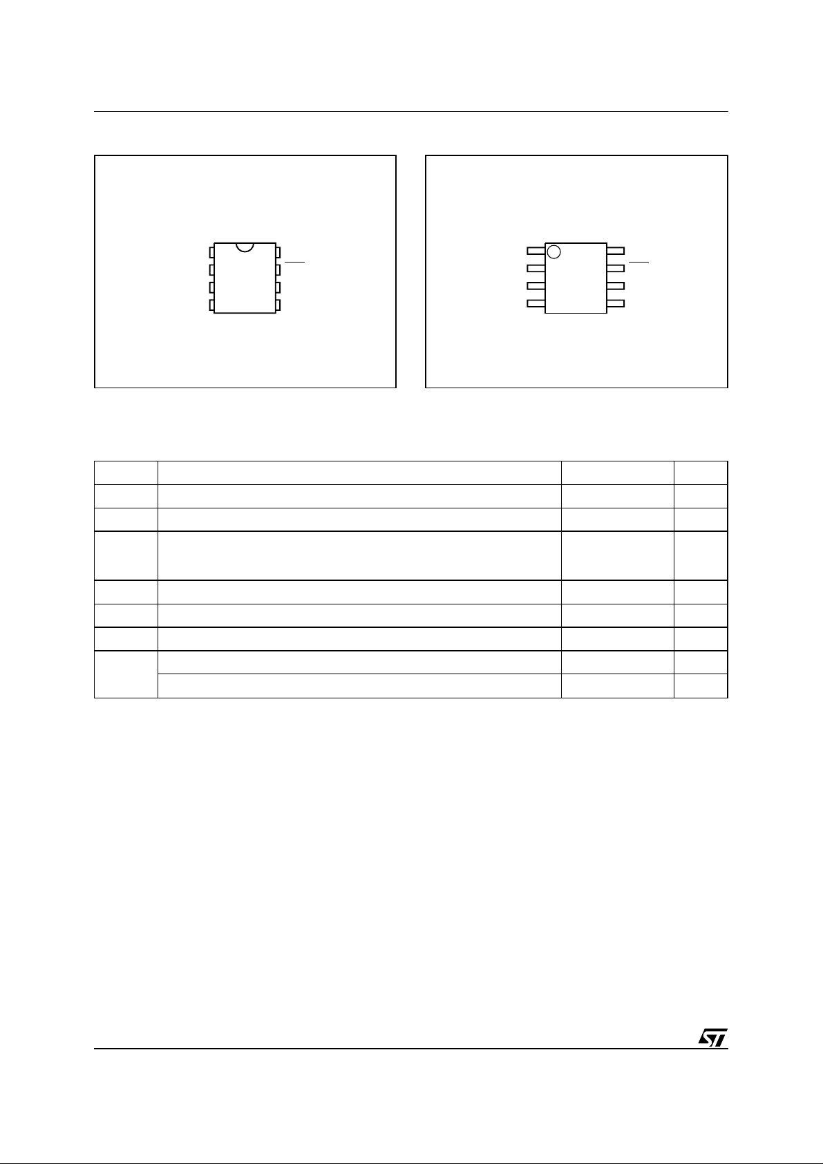
Figure 1. Logic Diagram
V
CC
WC
M2201
M2201
8
1
SO8 (M)
150mil Width
1
SDASCL
SDA Serial Data Input/Output
SCL Serial Clock
WC Write Control
V
CC
V
SS
July 1999 1/15
Supply Voltage
Ground
V
SS
AI01321
M2201
Figure 2A. DIP Pin Connections
M2201
1
NC V
2
3
NC
4
SS
Warning:
NC = Not Connected.
Tabl e 2. Absolute Maximum Ratings
Symbol Parameter Value Unit
T
T
T
STG
LEAD
Ambient Operating Temperature –40 to 85
A
Storage Temperature –65 to 150
Lead Temperature, Soldering (SO8 package)
8
7
6
5
AI01322
CC
WCNC
SCL
SDAV
(1)
(PSDIP8 package)
(TSSOP8 package)
Figure 2B. SO and TSSOP Pin Connections
M2201
AI01323
8
7
6
5
CC
WCNC
SCL
SDAV
215
260
t.b.c.
Warning:
NC V
1
2
NC
SS
NC = Not Connected.
40 sec
10 sec
t.b.c.
3
4
C
°
C
°
C
°
V
V
V
V
ESD
Notes:
DESCRIPTION (cont’d)
Output Voltage –0.6 to 6.5 V
O
Input Voltage –0.6 to 6.5 V
I
Supply Voltage –0.3 to 6.5 V
CC
Electrostatic Discharge Voltage (Human Body model)
Electrostatic Discharge Voltage (Machine model)
1. Except for the rating "Operating Temperature Range", stresses above those listed in the T able "Absolute Maximum Ratings"
may cause permanent damage to the device. These are stress ratings only and operation of the device at these or any other
conditions above those indicated in the Operating sections of this specification is not implied. Exposure to Absolute Maximum
Rating conditions for extended periods may affect device reli ability. Refer also t o the STMicro ele ct ro nics SURE Prog ra m and other
relevant quality documents.
2. MIL-STD-883C, 3015.7 (100pF, 1500 Ω).
3. EIAJ IC-121 (Condition C) (200pF , 0 Ω).
(2)
(3)
4000 V
500 V
write operations during power up, a Power On
Reset (POR) circuit is implemented. Until the V
When writing data to the memory , it responds to the
8 bits received by asserting an acknowledge bit
during the 9th bit time. When data is read by the
bus master, it acknowledges the receipt of the data
bytes in the same way. Data transfers are terminated with a STOP condition.
Power On Reset: V
lock out write protect . In
CC
order to prevent data corruption and inadvertent
voltage has reached the POR threshold value, the
internal reset is active, all operations are disabled
and the device will not respond to any c ommand.
In the same way, when V
drops down from the
CC
operating voltage to below the POR threshold
value, all operations are disabled and the dev ice
will not respond to any command. A stable V
must be applied before applying any logic signal.
CC
CC
2/15
M2201
SIGNAL DESCRIPTIONS
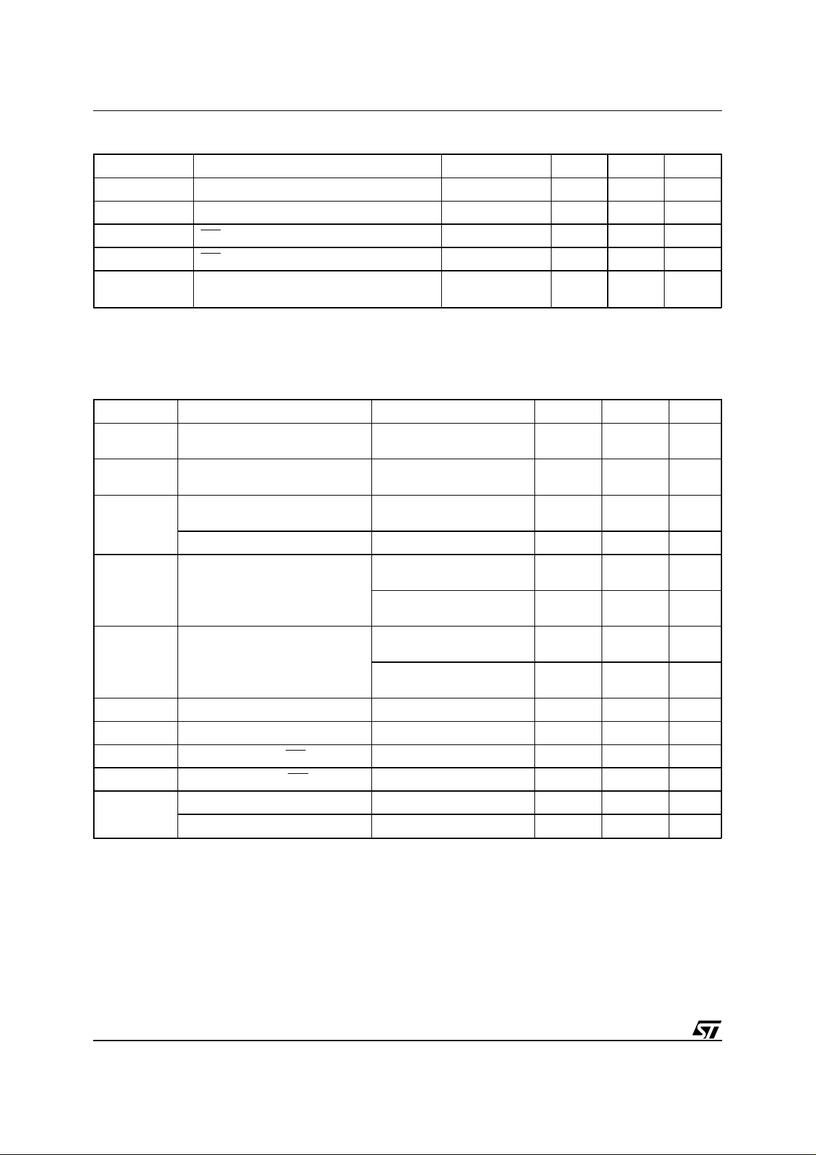
Serial Clock (SCL). The SCL input pin is used to
synchronize all data in and out of the memory. A
resistor can be connected from the SCL line to V
CC
to act as a pull up (see Figure 3).
Serial Data (SDA). The SDA pin is bi-directional
and is used to transfer data in or out of the memory.
It is an open drain output that may be wire-OR’ed
with other open drain or open collector signals on
the bus. A resistor must be connected from the SDA
bus line to V
Write Control (
feature (
to act as pull up (see Figure 3).
CC
WC). An hardware Write Control
WC) is offered on pin 7. This feature is
usefull to protect the contents of the memory from
any erroneous erase/write cycle. The W rite Control
signal is used to enable (
) the internal write protection. When uncon-
= V
IL
nected, the
WC input is internally read as VIL (WC
WC = VIH) or disable (WC
is disabled).
DEVICE O PERATION
The device that controls the data transfer is known
as the master. The master will alw ays initiate a data
transfer and will provide the serial clock for synchronisation. The M2201 is always a slave device
in all communications.
Start Condition. START is identified by a high to
low transition of the SDA line while the clock SCL
is stable in the high state. A ST AR T condition must
precede any command for data transfer. Except
during a programming cycle, the M2201 continuously monitor the SDA and SCL signals for a
START condition and will not respond unless one
is given.
Stop Condition. STOP is identified by a low to high
transition of the SDA line while the clock SCL is
stable in the high state. A STOP condition terminates communication between the M2201 and the
bus master . A S TOP condition at the end of a Read
command forces the standby state. A STOP c ondition at the end of a Write command triggers the
internal EEPROM write cycle.
Acknowledge Bit (ACK). An acknowledge signal
is used to indicate a successfull data transfer. The
bus transmitter, eit her master or s lave, will r elease
the SDA bus after sending 8 bits of data. During the
9th clock pulse period the receiver pulls the SDA
bus low to acknowledge the receipt of the 8 bits of
data.
Data Input. During data input the M2201 sample
the SDA bus signal on the rising edge of the clock
SCL. Note that for correct device operation the SDA
signal must be stable during the clock low to high
transition and the data must change ONLY when
the SCL line is low.
Figure 3. Maximum RL Value versus Bus Capacitance (C
20
16
12
max (kΩ)
L
R
8
4
0
VCC = 5V
100 200 300 400
C
(pF)
BUS
)
BUS
V
MASTER
CC
SDA
SCL
C
BUS
R
L
C
BUS
AI01100
R
L
3/15
M2201
T able 3. Input Parameters (T
= 25 °C, f = 100 kHz )
A
Symbol Parameter Test Condition Min Max Unit
C
IN
C
IN
(1)
Z
WCL
(1)
Z
WCH
(1)
t
LP
Note:
1. The results come from simulation, actual results may vary. These figures are not guaranteed.
Input Capacitance (SDA) 8 pF
Input Capacitance (other pins) 6 pF
WC Input Impedance VIN ≤ 0.3 V
WC Input Impedance VIN ≥ 0.7 V
Low-pass filter input time constant
(SDA and SCL)
CC
CC
520k
500 k
100 ns
T ab le 4. DC Characteristics
(T
= 0 to 70 °C or –40 to 85 °C; VCC = 4.5V to 5.5V or 2.7V to 5.5V)
A
Symbol Parameter Test Condition Min Max Unit
I
I
I
CC1
I
CC2
V
V
V
V
V
I
CC
LO
LI
OL
Input Leakage Current
(SCL, SDA)
Output Leakage Current
Supply Current (M2201)
Supply Current (M2201V) V
0V ≤ V
0V ≤ V
V
= 5V; fC = 100kHz
CC
(Rise/Fall time < 30ns)
= 2.7V; fC = 100kHz 1 mA
CC
VIN = VSS or VCC,
Supply Current (Standby)
(M2201)
V
IN
V
= 5V, fC = 100kHz
CC
V
IN
Supply Current (Standby)
(M2201V)
IL
IH
IL
IH
Input Low Voltage (SCL, SDA) –0.3 0.3 V
Input High Voltage (SCL, SDA) 0.7 V
Input Low Voltage (WC) –0.3 0.5 V
Input High Voltage (WC) VCC – 0.5 VCC + 1 V
V
IN
= 2.7V; fC = 100kHz
V
CC
Output Low Voltage (M2201) IOL = 3mA, VCC = 5V 0.4 V
Output Low Voltage (M2201V) I
= 2mA, VCC = 2.7V 0.4 V
OL
≤ V
IN
CC
≤ VCC
OUT
SDA in Hi-Z
= 5V
V
CC
= VSS or VCC,
= VSS or VCC,
V
= 2.7V
CC
= VSS or VCC,
CC
2
±
2
±
2mA
100
300
5
50
CC
VCC + 1 V
Ω
Ω
A
µ
A
µ
A
µ
A
µ
A
µ
A
µ
V
4/15
T ab le 5. AC Characteristics
(T
= 0 to 70 °C or –40 to 85 °C; VCC = 4.5V to 5.5V or 2.7V to 5.5V)
A
Symbol Alt Parameter Min Max Unit
t
CH1CH2
t
CL1CL2
t
DH1DH2
t
DL1DL1
(1)
t
CHDX
t
CHCL
t
DLCL
t
CLDX
t
CLCH
t
DXCX
t
CHDH
t
DHDL
(2)
t
CLQV
t
CLQX
f
C
t
W
Notes:
1. For a reSTART condition, or following a write cycle.
2. The minimum value delays the falling/rising edge of SDA away from SCL = 1 in order to avoid unwanted START and/or STOP
conditions.
t
R
t
F
t
R
t
F
t
SU:STA
t
HIGH
t
HD:STA
t
HD:DAT
t
LOW
t
SU:DAT
t
SU:STO
t
BUF
t
AA
t
DH
f
SCL
t
WR
Clock Rise Time 1
Clock Fall Time 300 ns
Input Rise Time 1
Input Fall Time 300 ns
Clock High to Input Transition 4.7
Clock Pulse Width High 4
Input Low to Clock Low (START) 4
Clock Low to Input Transition 0
Clock Pulse Width Low 4.7
Input Transition to Clock Transition 250 ns
Clock High to Input High (STOP) 4.7
Input High to Input Low (Bus Free) 4.7
Clock Low to Next Data Out Valid 0.3 3.5
Data Out Hold Time 300 ns
Clock Frequency 100 kHz
Write Time 10 ms
M2201
s
µ
s
µ
s
µ
s
µ
s
µ
s
µ
s
µ
s
µ
s
µ
s
µ
T ab le 6. AC Measurement Conditions
Input Rise and Fall Times
Input Pulse Voltages 0.2V
Input and Output Timing Ref.
Voltages
50ns
≤
0.3V
to 0.8V
CC
to 0.7V
CC
CC
CC
Figure 4. AC Testing Input Output Waveforms
0.8V
0.2V
CC
CC
0.7V
0.3V
AI00825
CC
CC
Memory Addressing. T o start communication between the bus master and the slave M2201, the
master must initiate a START condition. Following
this, the master sends onto the SDA bus line 8 bits
(MSB first) corresponding to the 7th bit byte- address and a READ or WRITE bit. This 8th bit is set
to ’1’ for read and ’0’ for write operations. If a match
is found, the corresponding memory will acknowledge the identification on the SDA bus during the
9th bit time.
Write Operations
Following a ST A RT condition the m aster sends t he
byte address with the R
W bit reset to ’0’. The
memory acknowledges this and waits for a data
byte. Any write command with
WC = 1 (during a
period of time from the START condition until the
end of the Byte Address) will not modify data and
will NOT be acknowledged on data bytes, as in
Figure 8.
5/15
 Loading...