


SGS Thomson Microelectronics M14C32, M14C64 Datasheet
M14C64
M14C32
Memory Card IC
64/32 Kbit Serial I²C Bus EEPROM
■ Compat ible with I
■ Two Wire I
2
C Extended Addressing
2
C Serial Interface
Supports 400 kHz Protocol
■ Single Supply Voltage (2.5 V to 5.5 V)
■ Hardware Write Control
■ BYTE and PAGE WRITE (up to 32 Bytes)
■ BYTE, RANDOM and SEQUENTIAL READ
Modes
■ Self-Tim e d P ro g ra m ming Cycle
■ Automatic Address Incrementing
■ Enhanced ESD/Latch-Up Behaviour
■ 1 Million Erase/Write Cycles (minimum)
■ 40 Year Data Retention (minimum)
■ 5 ms Programming Time (typical)
DESCRIPTION
Each device is an electrically erasable program mable memory (EEPROM) fabricated with STMi-
croelectronics’s High Endurance, Single
Polysilicon, CMOS technology. This guarantees
an endurance typically well above one million
Erase/Write cycles, with a data retention of
40 years. The memory operates with a power supply as low as 2.5 V.
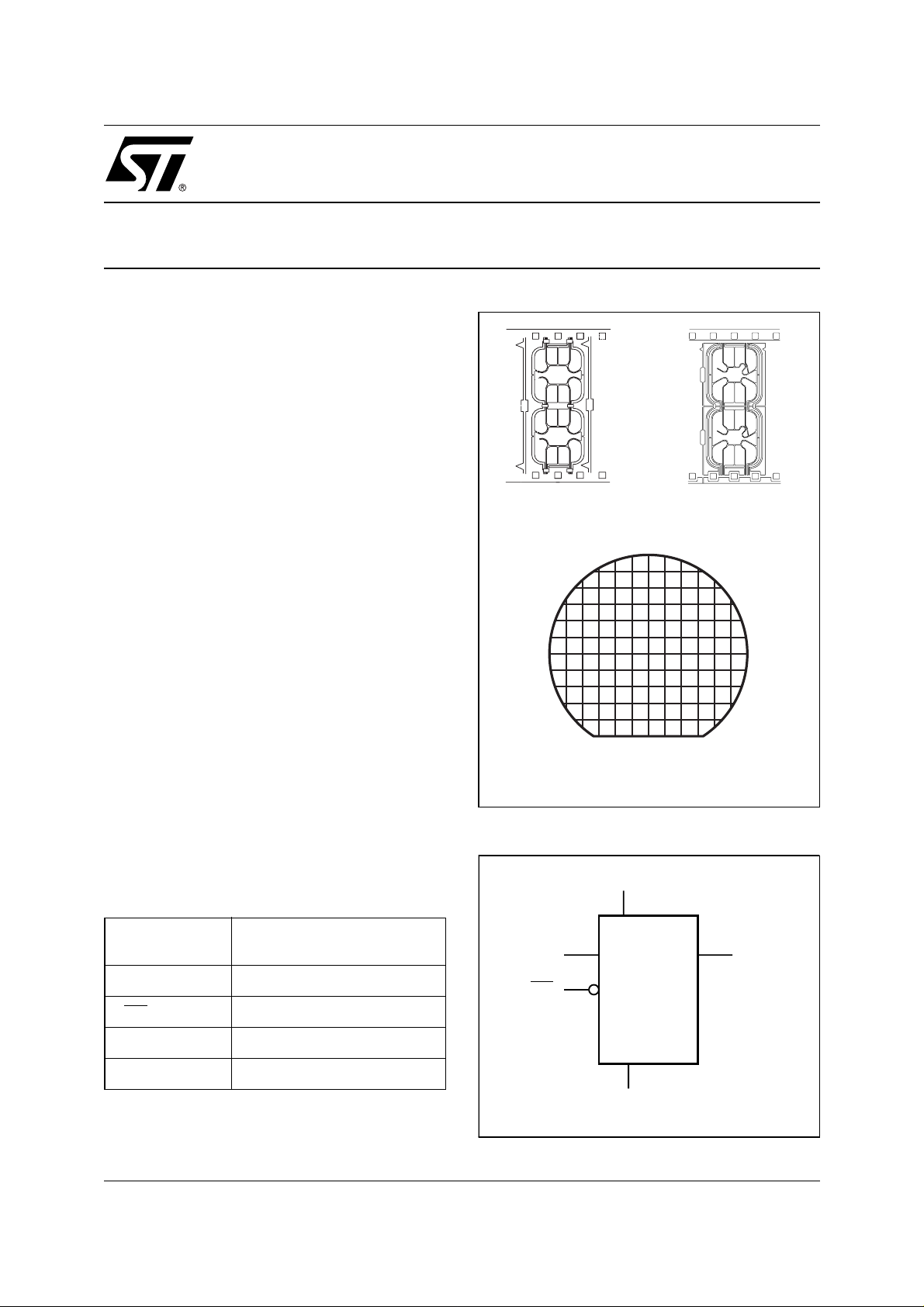
The M14C32 is available in wafer form (either
sawn or unsawn) and in micromodule form (on
film). The M14C64 is available in micro-module
2
2
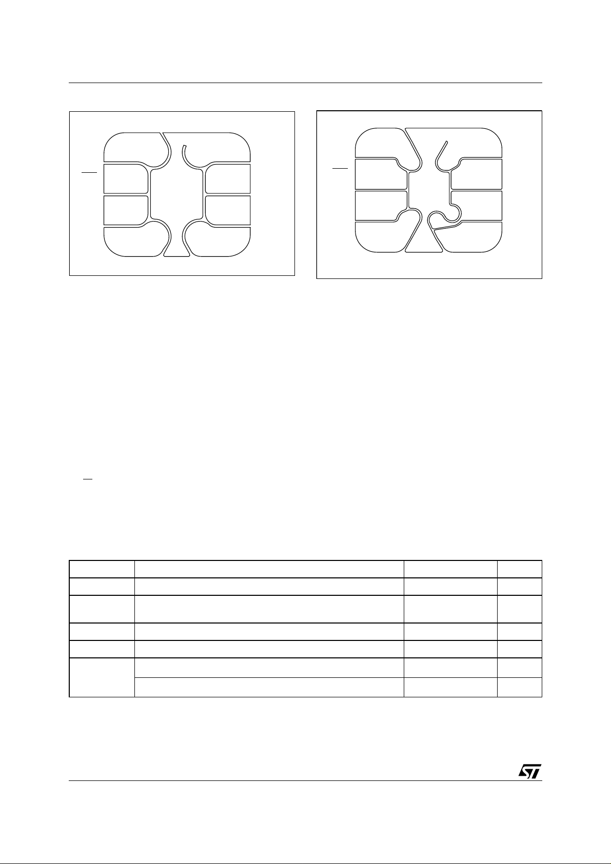
Micromodule (D20)
2
2
Wafer
Figure 1. Logic Diagram
Micromodule (D22)
Table 1. Signal Names
SDA Serial Data/Address Input/
Output
SCL Serial Clock
WC
V
CC
GND Ground
Write Control
Supply Voltage
SCL
V
CC
GND
SDA
M14xxxWC
AI02217
1/14October 1999
M14C64, M14C32
Figure 2. D20 Contact Connections
V
CC
GND
WC
SCL
SDA
AI02168
form only. For availability of the M14C64 in wafer
form, please contact your ST sales office.
Each memory is compatible with the I
2
C extended
memory standard. This is a two wire serial interface that uses a bi-directional data bus and serial
clock. The memory carries a built-in 7-bit unique
Device Type Identifier code (1010000) in accordance with the I
can be attached to each I
The memory behaves as a slave device in the I
2
C bus definition. Only one memory
2
C bus.
2
protocol, with all memory operations synchronized
by the serial clock. Read and write o perations are
initiated by a START condition, gene rated by the
bus master. The STA RT condition is followed by
the Device Select Code which is compos ed of a
stream of 7 bits (1010000), plus one read/write bit
(R/W
) and is terminated by an acknowledge bit.
When writing data to the memory, the mem ory inserts an acknowledge bit during the 9
th
bit time,
Figure 3. D22 Contact Connections
V
CC
WC
SCL
following the bus master’s 8-bit transmission.
When data is read by the bus master, the bus
master acknowledges the receipt of the data byte
in the same way. Data transfers are terminated by
a STOP condition after an Ack for WRITE, and after a NoACK for READ.
Power On Reset: V
Lock-Out Write Protect
CC
In order to prevent data corruption and inadvertent
write operations during power up, a Power On Re-
C
set (POR) circuit is included. The internal reset is
held active until the V
voltage has reached the
CC
POR threshold value, and all operations are disabled – the device will not respond to any command. In the same way, when V
drops from the
CC
operating voltage, below the POR threshold value,
all operations are disabled and the device will not
respond to any com ma nd. A s table a nd v alid V
must be applied before applying any logic signal.
GND
SDA
AI02204
CC
Table 2. Absolute Maximum Ratings
Symbol Parameter Value Unit
T
A
T
STG
V
IO
V
CC
V
ESD
Note: 1. Exc ept for the rating “Operating Temperature Range”, stresses above those l i sted in the Table “Absolute Maximum Ratings” may
2/14
cause permanent damage to the device. These are stress ratings only, and operation of the device at these or any other conditions
above those indica te d i n the Operating secti ons of this specification is not im plied. Exposure to Absolute Ma xim um Rating conditions for extended periods may affect device reliability. Refer also to the ST SURE Program and other relevant quality documents.
2. MIL -STD-883C, 3015.7 (100 pF, 1500 Ω )
3. EIA J I C-121 (Condi tion C) (200 pF, 0 Ω)
Ambient Operating Temperature 0 to 70 °C
Storage Temperature
Input or Output range -0.6 to 6.5 V
Supply Voltage -0.3 to 6.5 V
Electrostatic Discharge Voltage (Human Body model)
Electrostatic Discharge Voltage (Machine model)
1
Wafer form
Module form
2
3
-65 to 150
-40 to 120
4000 V
400 V
°C
M14C64, M14C32
SIGNAL DESCRIPTION
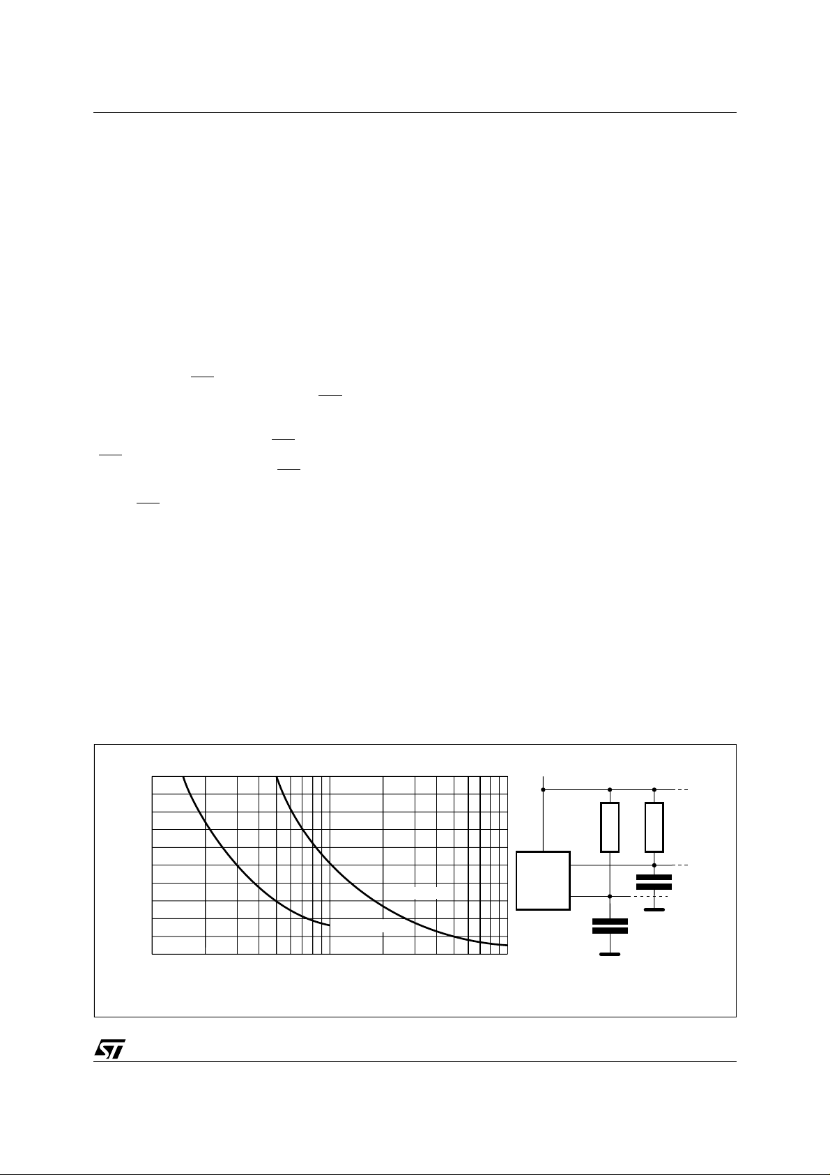
Serial Clock (SCL)
The SCL input pin is used to sync hronize all data
in and out of the memory. A pull up resistor can be
connected from the SCL line to V
. (Figure 4 in-
CC
dicates how the value of the pull-up resistor can be
calculated).
Serial Data (SDA)
The SDA pin is bi-directional, and is used to transfer data in or out of the memory. It is an open drain
output that may be wire-OR’ed with other open
drain or open collector signals on the bus. A pull
up resistor must be connected from the SDA bus
to V
. (Figure 4 indicates how the value of the
CC
pull-up resistor can be calculated).
Write Control (WC
The hardware Write Control contact (WC
)
) is useful
for protecting the entire contents of the memory
from inadvertent erase/write. The Write Control
signal is used to enable (WC
(WC
=VIH) write instructions to the entire memory
area. When unconnected, the WC
ly read as V
When WC
and write operations are allowed.
IL
=1, Device Select and Address bytes
=VIL) or disable
input is internal-
are acknowledged, Data bytes are not acknowledged.
Please see the Application Note
AN404
for a more
detailed description of the Write Control feature.
DEVICE OPERATION
2
The memory device supports the XI
2
I
C) protocol, as summarized in Figure 5. Any de-
C (Extended
vice that sends data on to the bus is defined to be
a transmitter, and any dev ice that reads the dat a
to be a receiver. The device that controls the data
transfer is known as the master, and the other as
the slave. A data transfer can o nly be initiated by
the master, which will also provide the serial clock
for synchronization. The memory device is always
a slave device in all communication.
Start Condition
START is identified by a high t o low transition of
the SDA line while the clock, SCL, is stable i n the
high state. A START condition must precede any
data transfer comman d. Th e m em ory devi ce continuously monitors (except during a program ming
cycle) the SDA and SCL lines for a START condition, and will not respond unless one is given.
Stop Condition
STOP is identified by a low to high transition of the
SDA line wh ile th e clock S CL is sta ble in the h igh
state. A STO P condition terminates c ommunication between the memory device and the bus master. A STOP condition at the end of a Read
command, after (and only after) a NoACK , forces
the memory device into its standby state. A STOP
condition at the end of a Write command triggers
the internal EEPRO M writ e cycle.
Acknowledge Bit (ACK)
An acknowledge signal is used to indicate a successful data transfer. The bus transmitter, either
master or slave, will release the SDA bus after
sending 8 bits of data. During t he 9
th
clock pulse
period the receiver pulls the SDA bus low to acknowledge the receipt of the 8 data bits.
Data Input
During data input, the memory device samples the
SDA bus signal on the rising edge of the clock,
SCL. For correct device operation, the SDA signal
must be stable during the clock low-to-high transition, and the data must change
only
when the SCL
line is low.
Figure 4. Maximum R
20
16
12
8
Maximum RP value (kΩ)
4
0
10 1000
Value versus Bus Capacitance (C
L
fc = 100kHz
fc = 400kHz
100
C
(pF)
BUS
) for an I2C Bus
BUS
V
MASTER
CC
SDA
SCL
R
R
C
BUS
L
C
BUS
AI01665
3/14
L
M14C64, M14C32
2
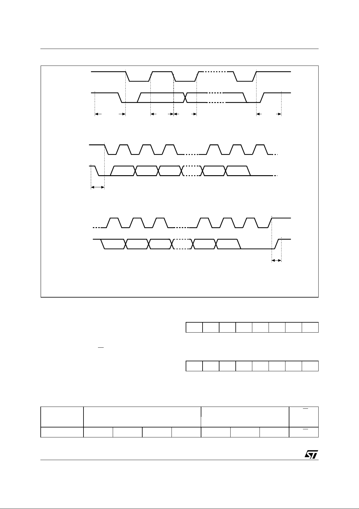
Figure 5. I
C Bus Protocol
SCL
SDA
SCL
SDA
SCL
SDA
START
CONDITION
START
CONDITION
SDA
INPUT
1 23 789
MSB
1 23 789
MSB ACK
SDA
CHANGE
CONDITION
ACK
STOP
STOP
CONDITION
AI00792
Memory Addressing
To start communication betwee n the bus master
and the slave memory, the master must initiate a
START condition. Following this, the master sends
8 bits to the SDA bus line (with the most significant
bit first). These bits represent the Device Select
Code (7 bits) and a RW
bit.
The seven most s ignificant bits of the Device Select Code are the Device Type Identifier, according
to the I
Table 5. Device Select Code
Note: 1. The most significant bit, b7, is sent first.
4/14
2
C bus definition. For the mem ory device,
1
Device Code Chip Enable RW
b7 b6 b5 b4 b3 b2 b1 b0
Device Select 1010000RW
Table 3. Most Significant Byte
b15 b14 b13 b12 b11 b10 b9 b8
Note: 1. b15 to b13 are Don’t Care on the M14C6 4 series.
b15 to b12 are Don’t Care on the M 14C32 serie s.
Table 4. Least Significant Byte
b7 b6 b5 b4 b3 b2 b1 b0
M14C64, M14C32
the seven bits are fixed at 1010000b (A0h), as
shown in Table 5.
th
The 8
bit is the read or write bit (RW). This bit is
set to ‘1’ for read and ‘0’ for write operations. If a
match occurs on the Device Select Code, the corresponding memory gives an acknowledgment on
the SDA bus during the 9
th
bit time. If the memory
does not match the Device Select code, it will deselect itself from the bus, and go into stand-by
mode.
Each data byte in the m emory has a 16-bit (two
byte wide) address. The Most Significant Byte (Table 3) is sent first, f ollowed by the Least significant
Byte (Table 4). Bits b15 to b0 form t he addre ss of
the byte in memory. Bits b15 to b13 are treated as
a Don’t Care bit on the M14C64 memory. Bits b15
to b12 are treated as Don’t Care bits on the
M14C32 me m o r y .
Write Operations
Following a START con dition the ma ster sends a
Device Select code with the RW
bit set to ’0’, as
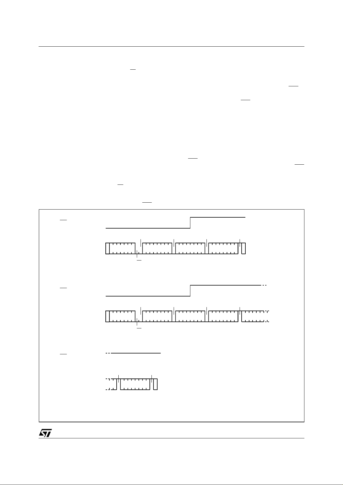
Figure 6. Wri te Mo de S e qu e nces with WC=1
WC
shown in Table 6. The memory acknowledges it
and waits for two bytes of address, which provides
access to the memory area. After receipt of each
byte address, the memory again responds with an
acknowledge and waits for t he data byte. Writing
in the memory may be inhibited if input pin WC
is
taken high.
Any write command with WC
=1 (during a period of
time from the START condition until the end of the
two bytes address) will not modify the memory
content and will NOT be acknowledged on data
bytes, as shown in Figure 6.
Byte Write
In the Byte Write mode, after the Device Select
code and the address, the master sends one data
byte. If the addressed location is write protected by
the W C
pin, the memory replies with a NoACK,
and the location is not modified. If, instead, the WC
pin has been held at 0, as shown in F igure 7, the
memory replies with an ACK. The master terminates the transfer by generating a STOP condition.
ACK ACK ACK NO ACK
BYTE WRITE DEV SEL BYTE ADDR BYTE ADDR DATA IN
R/W
START
WC
ACK ACK ACK NO ACK
PAGE WRITE DEV SEL BYTE ADDR BYTE ADDR DATA IN 1
R/W
START
WC (cont'd)
NO ACK NO ACK
PAGE WRITE
(cont'd)
DATA IN N
STOP
DATA IN 2
STOP
AI01120B
5/14