DD.M14C04/9811V1.1 1/2
M14C04 DD
M14C04 Die Description
PRODUCT M14C04
■ WAFER SIZE 152 mm (6 inches)
■ DIE IDENTIFICATION M14C04KA_R
■ DIE SIZE (X x Y) 1465 x 1585 µm
■ SCRIBE LINE 101.6 x 101.6 µm
■ PAD OPENING 100 x 100 µm
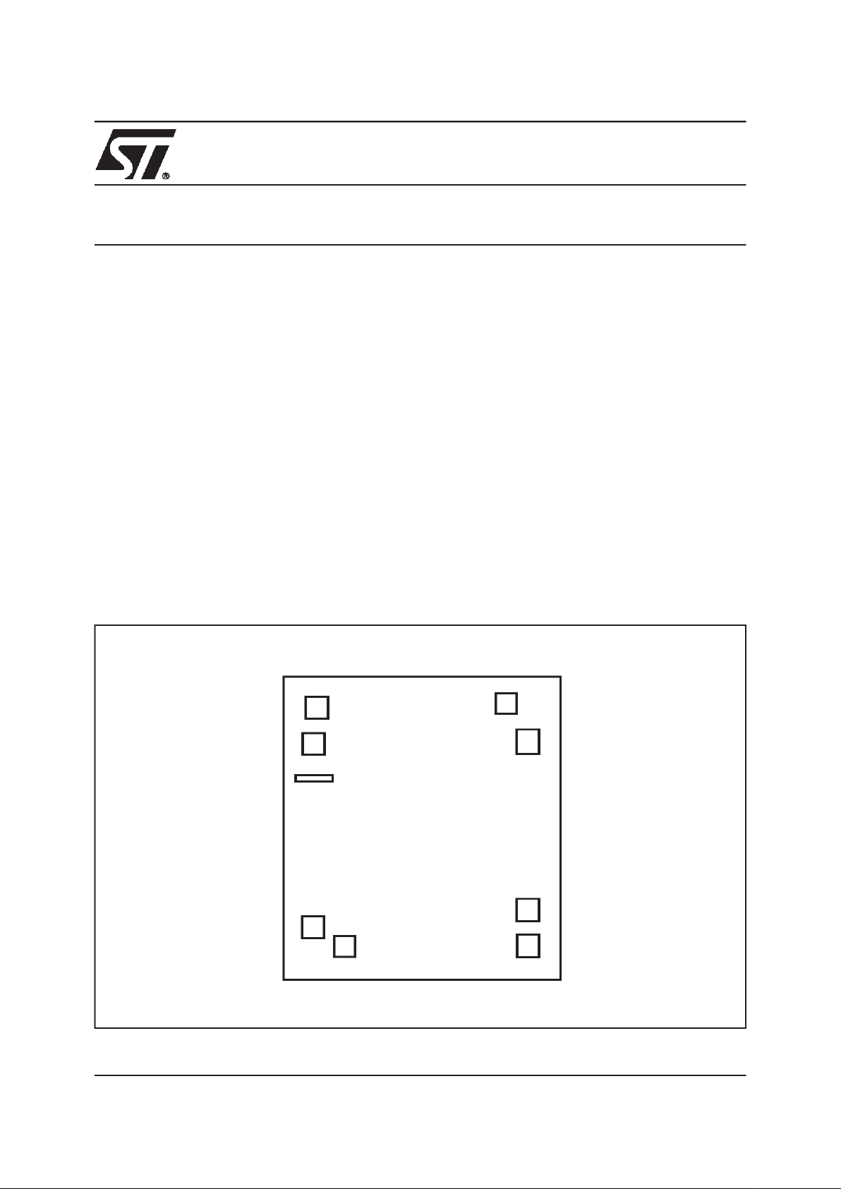
DIE LAYOUT
■ DI Die Identification (at the position shown in Figure 1)
■ C1, C2, C3, C5, C7 Pad contacts to the ISO pins (at the positions shown in Figure 1)
■ C4, C6, C8 These ISO pins do not appear on the M14C04 die
■ NC This pad, shown in Figure 1, is Not Connected
Pad locations are measured relative to the die centre (where X and Y are respectively the horizontal and
vertical axis, measured in µm).
Figure 1. M14C04 Die Plot
AI02497
C3: SCL
(X= –552.0; Y= –509.76)
C7: SDA (X= –532.3; Y= +609.6)
DI
NC: TEST
NC: TEST
NC: TEST
C5: GND (X= +442.8; Y= +626.0)
C2: WC (X= –386.96; Y= –609.76)
C1: VCC
(X= +551.9; Y= –605.0)

M14C04 DD
2/2
Information furnished is believed to be accurate and reliable. However, STMicroelectronics assumes no responsibility for the consequences
of useof such information norfor any infringement of patents or other rights of thirdparties which may result from itsuse. No license isgranted
by implication or otherwise under any patent or patent rights of STMicroelectronics. Specifications mentioned in this publication are subject
to change without notice. This publication supersedes and replaces all information previously supplied. STMicroelectronics products are not
authorized for use as critical components in life support devices or systems without express writtenapproval of STMicroelectronics.
1998 STMicroelectronics - All Rights Reserved
The ST logo is a registered trademark of STMicroelectronics.
All other names are the property of their respective owners.
STMicroelectronics GROUP OF COMPANIES
Australia - Brazil - China - France - Germany - Italy - Japan - Korea - Malaysia - Malta - Mexico - Morocco - The Netherlands - Singapore -
Spain - Sweden - Switzerland - Taiwan - Thailand - United Kingdom - U.S.A.
http://www.st.com
 Loading...