

.
LOW POWERCONSUMPTION
.
SHORT CIRCUIT PROTECTION
.
LOW DISTORTION,LOW NOISE
.
HIGHGAIN-BANDWIDTH PRODUCT
.
HIGHCHANNEL SEPARATION
LS204
HIGH PERFORMANCE
DUALOPERATIONAL AMPLIFIERS
DESCRIPTION
The LS204is a highperformance dual operational
amplifier with frequency and phase compensation
builtintothechip.Theinternalphasecompensation
allows stable operation as voltagefollowerin spite
of itshigh Gain-BandwidthProduct.
The circuit presents very stable electrical characteristics over the entire supply voltage range, and
is particularlyintendedforprofessionalandtelecom
applications(activefilter, etc).
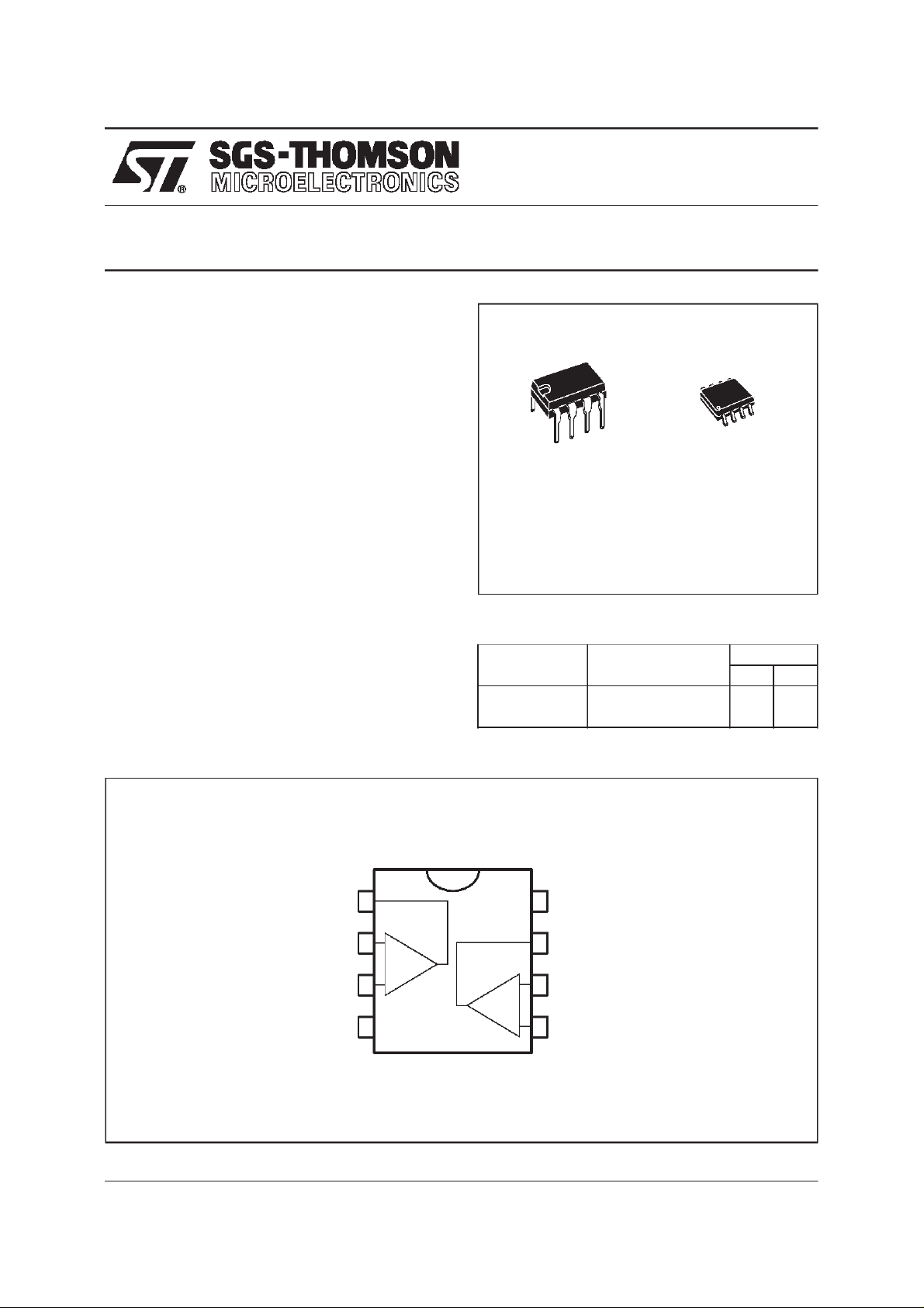
PINCONNECTIONS (top view)
Output 1
1
N
DIP8
(Plastic Package)
ORDER CODES
Part Number Temperature Range
LS204C 0, +70
LS204I -40, +105
8
V
CC
(Plastic Micropackage)
o
C ••
o
+
D
SO8
Package
ND
C ••
April 1998
Inverting Input 1
Non-inverting Input 1
CCV
Output
2
3
-
4
-
+
-
+
7
Non-inverting Input 2
6
Inverting Input 2
5
1/10
LS204
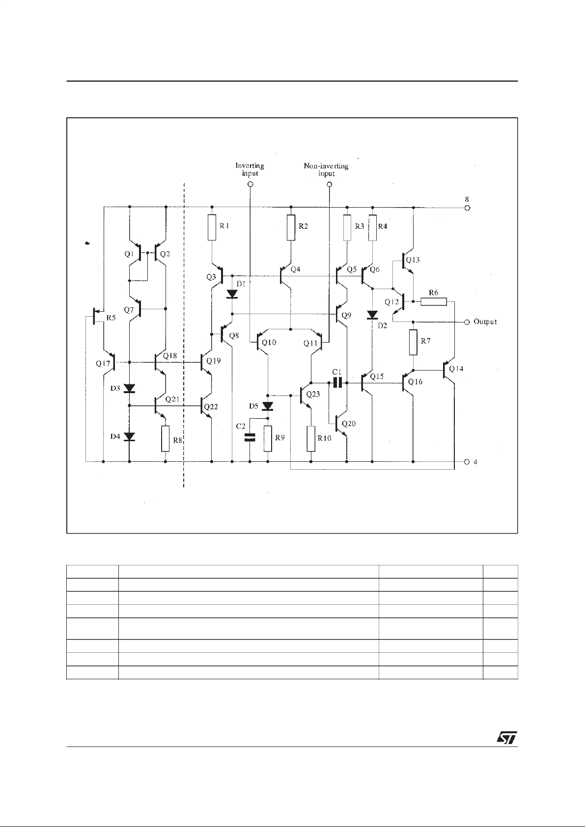
SCHEMATIC DIAGRAM (1/2 LS204)
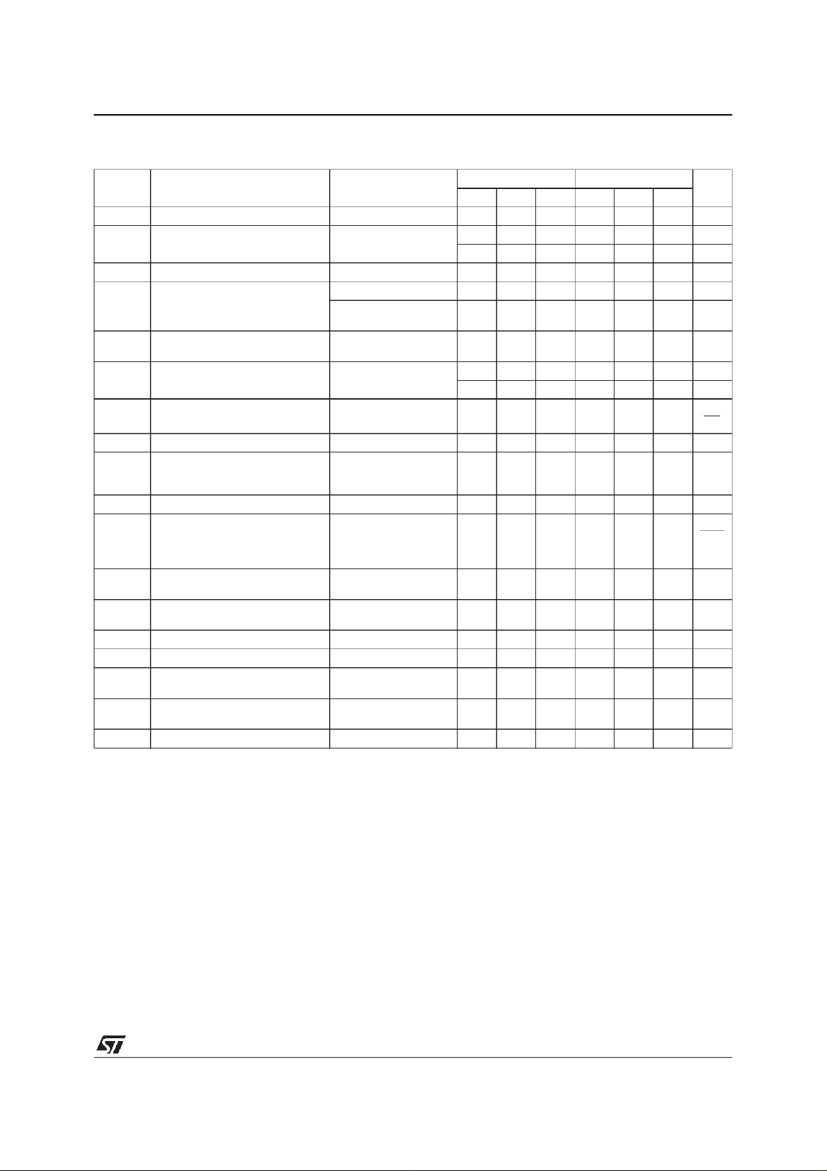
ABSOLUTEMAXIMUM RATINGS
Symbol Parameter Value Unit
SupplyVoltage ±18 V
InputVoltage ±V
i
Differential Input Voltage ± (VCC-1)
id
Operating Temperature Range LS204C
LS204I
Power Dissipation at T
JunctionTemperature 150
j
=70oC 500 mW
amb
CC
0 to +70
-40 to +105
Storage Temperature Range -65 to +150
2/10
V
CC
V
V
T
oper
P
tot
T
T
stg
o
C
o
C
o
C
LS204
ELECTRICALCHARACTERISTICS (VCC= ±15V,T
Symbol Parameter Test Conditions
Supply Current 0.7 1.2 0.8 1.5 mA
I
CC
Input Bias Current 50 150 100 300 nA
I
ib
T
min.<Top<Tmax
Input Resistance f = 1kHz 1 1 MΩ
R
i
Input Offset Voltage Rs≤ 10kΩ 0.5 2.5 0.5 3.5 mV
V
io
≤ 10kΩ
R
s
.<Top<T
T
min
DV
DI
Input Offset VoltageDrift Rs≤ 10kΩ
io
I
Input OffsetCurrent 5 20 12 50 nA
io
Input OffsetCurrent Drift T
io
Output Short Circuit Current 23 23 mA
I
os
Large Signal Voltage Gain T
A
vd
.<Top<T
T
min
.<Top<T
T
min
.<Top<T
min
.<Top<T
min
=2kΩ VCC= ±15V
R
L
V
= 25oC, unless otherwisespecified)
amb
LS204I LS204C
Min. Typ. Max. Min. Typ. Max.
. 300 700 nA
. 3.5 5
max
.2 2
max
. 40 100 nA
max
. 0.08 0.1 nA
max
.
CC
max
= ±4V
90 100
95
86 100
95
GBP Gain-Bandwidth Product f = 100kHz 1.8 3 1.5 2.5 MHz
Equivalent Input Noise Voltage f = 1kHz
e
n
THD Total Harmonic Distortion A
±V
V
Output Voltage Swing RL=2kΩ VCC= ±15V
opp
Large Signal Voltage Swing RL= 10kΩ f = 10kHz 28 28 V
opp
=50Ω
R
s
=1kΩ
R
s
= 10kΩ
R
s
= 20dB RL=2kΩ
V
=2VPPf = 1kHz
V
O
V
CC
= ±4V
8
15 10
10
18
12
20
0.03 0.1 0.03 0.1 %
±13
±3
±13
±3
SR Slew Rate Unity Gain, RL=2kΩ 0.8 1.5 1 V/µs
CMR Common Mode Rejection Ratio V
SVR Supply Voltage Rejection Ratio V
V
O1/VO2
Channel Separation f = 1kHz 100 120 120 dB
= 10V
ic
.<Top<T
T
min
= 1V f = 100Hz
ic
.<Top<T
T
min
.90 86
max
.90 86
max
Unit
mV
µV/
√Hz
°C
dB
nV
V
dB
dB
PP
o
C
3/10

LS204
4/10

LS204
5/10

LS204
APPLICATION INFORMATION :
Active low-pass filter
BUTTERWORTH
The Butterworth is a ”maximally flat” amplitude
response filter (figure 10) Butterworth filters are
used forfilteringsignalsindataacquisitionsystems
to preventaliasing errors in samples-dataapplications and forgeneralpurpose low-pass filtering.
The cut-off frequencyF
, is the frequency at which
c
the amplitude responseis down 3dB. The attenuation ratebeyondthecutofffrequencyisn6 dB per
octave of frequencywhere n is the order (number
of poles)of the filter.
Other characteristics:
.
Flattestpossible amplitude response
.
Excellentgain accuracyat low frequencyend
of passband
BESSEL
The Bessel is a type of ”linear phase” filter. Because of their linear phase characteristics, these
filters approximate a constant time delay over a
limited frequency range. Bessel filters pass transientwaveformswithaminimumofdistortion.They
are also used to provide time delays for low pass
filteringof modulatedwaveformsand asa”running
average” type filter.
−n
The maximumphase shift is
Π
radianswhere n
2
is the order (number of poles) of the filter. The
cut-off frequencyf
, isdefined as the frequencyat
c
which the phase shift is one half of this value. For
accurate delay, the cut-off frequency should be
twice the maximum signal frequency.
The followingtable can beused to obtainthe -3dB
frequency of the filter.
2 Pole 4 Pole 6 Pole 8 Pole
-3dB Frequency 0.77f
0.67fc 0.57fc 0.50fc
c
Other characteristics:
.
Selectivitynot as great as Chebyschev or Butterworth
.
Verylittle overshoot response to step inputs
.
Fast rise time
CHEBYSCHEV
Chebyschev filters have greater selectivity than
either Bessel ro Butterworth at the expense of
ripple in the passband(figure 11).
Chebyschev filters are normally designed with
peak-to-peakripple values from 0.2dB to 2dB.
Increasedripple in the passbandallowsincreased
attenuationabove thecut-off frequency.
The cut-off frequency is defined as the frequency
at which the amplitude response passes through
the specificedmaximumripplebandandenters the
stop band.
Other characteristics:
.
Greaterselectivity
.
Verynon-linearphase response
.
High overshoot responseto step inputs
The table below shows the typical overshoot and settlingtime response of the low pass filtersto a step input.
Number of
Poles
Butterworth 2
4
6
8
Bessel 2
4
6
8
Chebyschev (ripple ±0.25dB) 2
4
6
8
Chebyschev (ripple ±1dB) 2
4
6
8
Design of 2ndorder activelow pass filter (Sallen and Key configuration unity gain-op-amp)
6/10
Peak
Overshoot
% Overshoot ±1% ±0.1% ±0.01%
4
11
14
16
0.4
0.8
0.6
0.1
11
18
21
23
21
28
32
34
Settling Time (% of final value)
1.1F
1.7/f
2.4/f
3.1/f
0.8/f
1.0/f
1.3/f
1.6/f
1.1/f
3.0/f
5.9/f
8.4/f
1.6/f
4.8/f
8.2/f
11.6/f
sec.
c
c
c
c
c
c
c
c
c
c
c
c
c
c
c
c
1.7Fcsec.
2.8/f
c
3.9/f
c
5.1/f
c
1.4/f
c
1.8/f
c
2.1/f
c
2.3/f
c
1.6/f
c
5.4/f
c
10.4/f
c
16.4/f
c
2.7/f
c
8.4/f
c
16.3/f
c
24.8/f
c
1.9Fcsec.
3.8/f
c
5.0/f
c
7.1/f
c
1.7/f
c
2.4/f
c
2.7/f
c
3.2/f
c
-
-
-
-
-
-
-
-

LS204
7/10

LS204
8/10

PACKAGE MECHANICALDATA
8 PINS- PLASTICDIP
LS204
Dim.
A 3.32 0.131
a1 0.51 0.020
B 1.15 1.65 0.045 0.065
b 0.356 0.55 0.014 0.022
b1 0.204 0.304 0.008 0.012
D 10.92 0.430
E 7.95 9.75 0.313 0.384
e 2.54 0.100
e3 7.62 0.300
e4 7.62 0.300
F 6.6 0260
i 5.08 0.200
L 3.18 3.81 0.125 0.150
Z 1.52 0.060
Min. Typ. Max. Min. Typ. Max.
Millimeters Inches
9/10

LS204
PACKAGE MECHANICALDATA
8 PINS- PLASTICMICROPACKAGE (SO)
Dim.
Min. Typ. Max. Min. Typ. Max.
Millimeters Inches
A 1.75 0.069
a1 0.1 0.25 0.004 0.010
a2 1.65 0.065
a3 0.65 0.85 0.026 0.033
b 0.35 0.48 0.014 0.019
b1 0.19 0.25 0.007 0.010
C 0.25 0.5 0.010 0.020
c1 45
o
(typ.)
D 4.8 5.0 0.189 0.197
E 5.8 6.2 0.228 0.244
e 1.27 0.050
e3 3.81 0.150
F 3.8 4.0 0.150 0.157
L 0.4 1.27 0.016 0.050
M 0.6 0.024
S8
Information furnished is believed to be accurateand reliable. However, SGS-THOMSON Microelectronics assumes no responsibility
for the consequences of use of such information nor for anyinfringement of patents or otherrights of third parties which may result
from its use. No license is granted by implication or otherwise under any patent or patent rights of SGS-THOMSON Microelectronics.
Specifications mentioned in this publication are subject to change without notice. This publication supersedes and replaces all
information previouslysupplied. SGS-THOMSON Microelectronics products are not authorized for use as critical components in life
support devices or systems without express written approval of SGS-THOMSON Microelectronics.
o
(max.)
10/10
1998 SGS-THOMSON Microelectronics– Printed in Italy – All Rights Reserved
SGS-THOMSON Microelectronics GROUP OF COMPANIES
Australia - Brazil -Canada - China - France - Germany - Italy - Japan - Korea - Malaysia - Malta - Morocco
The Netherlands - Singapore - Spain - Sweden -Switzerland - Taiwan - Thailand - United Kingdom -U.S.A.
 Loading...