

®
ELECTRONIC TW O - TO NE R INGER
.
LOW CURRENT CONSUMPTION, IN ORDER
TO ALLOW THE P ARALLEL OPERATION O F 4
DEVICES
.
INTEGRATED RECTIFIER BRIDGE WITH
ZENER DIODES TO PROTECT AGAINST
OVERVOLTAGES
.
LITTLE EXTERNAL CIRCUITRY
.
TONE AND SWITC HING FREQUEN CIES ADJUSTABLE BY EXTERNAL COMPONENTS
.
INTEGRATED VOLTAGE AND CURRENT
HYSTERESIS
DESCRIPTION
LS1240A is a mon olith ic in tegrated circ uit de signed
to replace the mechanical bell in telephone sets in
connection with an electro-acoustical converter. It
can drive directly a piezoceramic converter (buzzer)or a dynam ic loudspe ak er .
The output current capability of LS1240A is higher
than standard ringer. For driving a dynamic loudspeaker LS 124 0A c an simply us e a dec oupling capacitor, thus elim inating the us ual trans f or m er .
No curre nt limitation is provided on the outpu t stage
of LS1240A, so a minimum load DC of 50 Ω is adviced, in s er ies with a proper c apac itor.
The two tone frequencies generated are switched
by an inte rnal oscillator in a fas t sequence and m ade
audible across an output amplifier in the loudspeaker, both tone frequencies and the switching
frequency c an be externally adj us t ed.
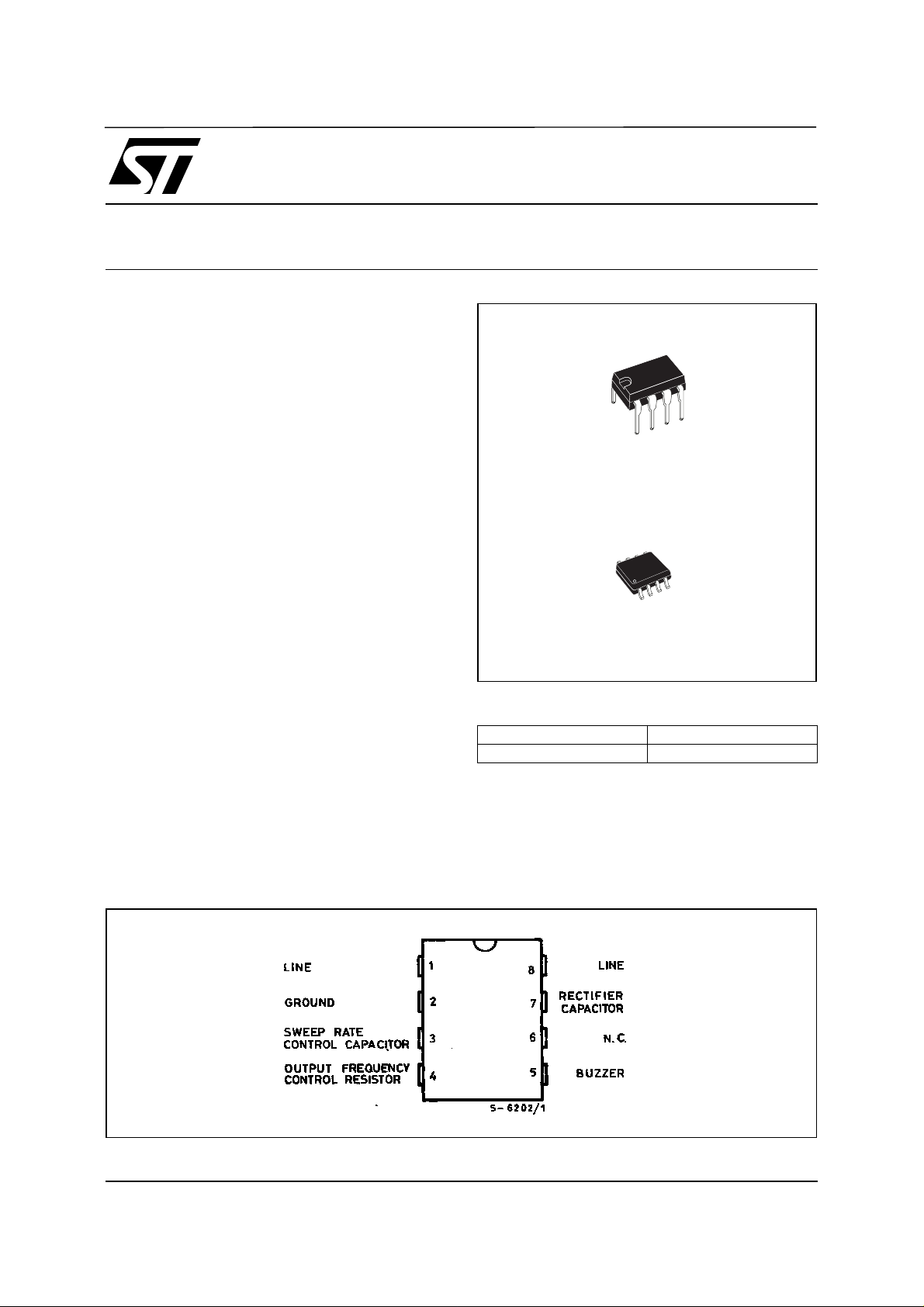
LS1240A
Minidip
SO8
ORDERING NUMBERS
Minidip SO8
LS1240A LS1240AD1
The suppl y voltage is obtained from the A C ring signal and the circuit is designed so that noise on the
line or variations of the ringing signal cannot affect
correct operation of the device.
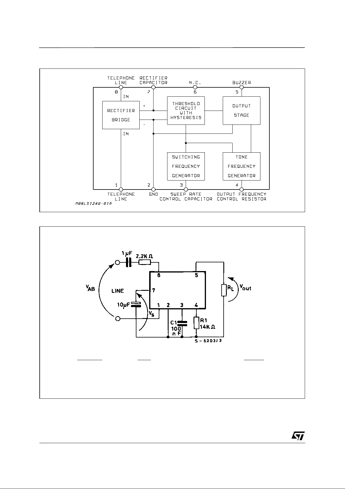
PIN CONNECTION (top view)
July 1998
1/7
LS1240A
BLOCK DIAGRAM
Figure 1 : Test Circuit.
2.72 ⋅ 10
R1 =
f1 (Hz)
4
⋅ (1 − 0.04 ln
f1
f2 = 0.725 f1 f
)
1943
SWEEP
=
C1 (nF)
750
2/7
LS1240A
ABSOLUTE MAXIMUM RATIN GS
Symbol Parameter Value Unit
V
AB
V
AB
DC Supply Current 30 mA
T
op
T
stg
THERMAL DATA
Symbol Parameter Value Unit
R
th j-amb
ELECTRICAL CHARACTERISTICS
= 25 °C; Vs = applied between pins 7-2 unless otherwise specified)
(T
amb
Symbol Parameter Test Conditions Min. Typ. Max. Unit
V
s
I
B
V
ON
V
OFF
R
D
V
OUT
I
OUT
AC OPERATION
f
1
f
2
f
SWEEP
Calling Voltage (f = 50 Hz) Continuous 120 V
Calling Voltage (f = 50 Hz) 5s ON/10s OFF 200 V
Operating Temperature – 40 to + 70
Storage and Junction Temperature – 65 to + 150
Thermal Resistance Junction-ambient Max 100
°
Supply Voltage 26 V
Current Consumption without Load (pins 8-1) V
= 9.3 to 25 V 1.5 1.8 mA
8-1
Activation Voltage 12.2 13.2 V
Sustaining Voltage 8 9 V
Differential Resistance in OFF Condition (pins 8-1) 6.4
Output Voltage Swing Vs – 5 V
Short Circuit Current (pins 5-2)
Output Frequencies
f
out1
f
out2
f
OUT1
f
OUT2
V
= 20V RL = 250
s
Vs = 26V, R1 = 14k
Vs = 0 V
= 6V
V
s
Ω
Ω
1.74
1.22
1.33 1.43
70 mA
2.14
1.6
Programming Resistor Range 8 56
Sweep Frequency
R
= 14kΩ, C1 = 100nF
1
5.25 7.5 9.75 Hz
rms
rms
C
°
C
°
C/W
k
kHz
k
Ω
Ω
3/7

LS1240A
Figure 2 : Typical Application wit h B UZZ E R
Figure 3 : T y pic al Ap plic ation with Lou ds peak er (no trans for me r ne eded)
C1 such that Z
LOAD
> 1 ΚΩ
4/7

MINIDIP PACKAGE MECHANICAL DATA
LS1240A
DIM.
MIN. TYP. MAX. MIN. TYP. MAX.
A 3.32 0.131
a1 0.51 0.020
B 1.15 1.65 0.045 0.065
b 0.356 0.55 0.014 0.022
b1 0.204 0.304 0.008 0.012
D 10.92 0.430
E 7.95 9.75 0.313 0.384
e 2.54 0.100
e3 7.62 0.300
e4 7.62 0.300
F 6.6 0.260
I 5.08 0.200
L 3.18 3.81 0.125 0.150
Z 1.52 0.060
mm inch
5/7

LS1240A
SO8 PACKAGE MECHANICAL DATA
DIM.
MIN. TYP. MAX. MIN. TYP. MAX.
A 1.75 0.069
a1 0.1 0.25 0.004 0.010
a2 1.65 0.065
a3 0.65 0.85 0.026 0.033
b 0.35 0.48 0.014 0.019
b1 0.19 0.25 0.007 0.010
C 0.25 0.5 0.010 0.020
c1
D (1) 4.8 5.0 0.189 0.197
E 5.8 6.2 0.228 0.244
e 1.27 0.050
e3 3.81 0.150
F (1) 3.8 4.0 0.15 0.157
L 0.4 1.27 0.016 0.050
M 0.6 0.024
S
mm inch
45° (typ.)
8° (max.)
6/7

LS1240A
Information furnished is believed to be accurate and reliable. However, STMicroelectronics assumes no responsibility for the consequences of use of such information nor for any inf ringement of patents or other rights of third parties which may result from its use. No
license is granted by implication or otherwise under any patent or patent rights of STMicroelectronics. Specification mentioned in this
publication are subject to change without notice. This publication supersedes and replaces all information previously supplied. STMicroelectronics products are not authorized for use as critical components in life support devices or systems without express written
approval of STMicroelec troni cs.
Australia - Brazil - Canada - C hina - F rance - Ger many - Ital y - Ja pan - Korea - Ma laysi a - Malta - M exic o - Morocco - The Net herlands -
Singapore - Spain - Sweden - S witzerl and - T aiwan - Thailand - Uni ted Kingdo m - U.S.A .
The ST logo is a regi stered tradem ark of ST Microe lectronics
© 1998 STMicroelectroni cs – Pri nted in Italy – All Rights R eserved
STMicr oe lect roni cs GROU P OF COMP AN IES
7/7
 Loading...