

Datasheet LM337SP, LM337K, LM237K, LM237SP, LM137K Datasheet (SGS Thomson Microelectronics)
NEGATIVE VOLTAGE REGULATORS
.OUTPUT VOLTAGEADJUSTABLE DOWN TO
V
ref
.1.5A GUARANTEEDOUTPUT CURRENT
.0.3%/V TYPICAL LOAD REGULATION
.0.01%/VTYPICAL LINE REGULATION
.CURRENT LIMIT CONSTANT WITH TEM-
PERATURE
.RIPPLE REJECTION : 77dB
.STANDARD 3-LEAD TRANSISTOR PACK-
AGES
.EXCELLENT THERMAL REGULATION:
0.002%/V
.50ppm/°C TEMPERATURE COEFFICIENT
DESCRI PTIO N
The LM137 series are adjustable 3-terminal negative voltage regulators capable of supplying in excess-1.5Aovera -1.2to -37Voutput voltagerange.
Theyare exceptionally easy touse andrequireonly
two externalresistors to settheoutput voltage. Further, both line and load regulation are better than
standard fixed regulators. Also, LM137 regulators
aresupplied in standard transistor packages which
are easily mounted and handled. In addition to
higher performance than fixed regulators, the
LM137series offer fulloverload protectionavailable
only in integrated circuits. Included on the chip are
current limit, thermal overload protection and safe
area protection. All overload protection circuitryremainsfullyfunctionaleveniftheadjustment terminal
is disconnected.
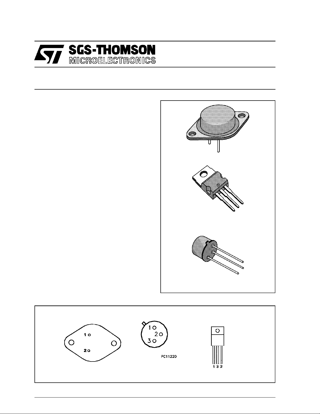
LM137/LM237
LM337
THREE-TERMINAL ADJUSTABLE
TO-3
TO-220
TO-39
PIN CONNECTIONS
(bottomview)
1 - Output
2 - Adj
Case is input
March1993
TO-3
TO-39
(bottomview)
1 - Adj
2 - Output
3 - input
TO-220
(frontview)
1 - Adj
2 - Output
3 - Input
Heatsink surface connected to input
1/14
LM137-LM237-LM337
ABSOLU TE MAXIMU M RAT ING
Symbol Parameter Value Unit
V
T
THERMA L CHA R ACTE R ISTI CS
Symbol Parameter Typ. Max. Unit
R
R
Input Output Voltage Differential 40 V
I-VO
Output Current TO-220/TO-3 1.5 A
I
O
TO-39 0.5
oper
LM137 -55 to 150
LM237 -25 to 150
LM337 0 to 125
T
stg
P
tot
Junction-case Thermal Resistance TO-3 4
thj-case
-65 to 150
Internally Limited W
TO-220 3
TO-39 15
Junction-ambient Thermal Resistance TO-3 35
thj-amb
TO-220 70
TO-39 160
o
o
C
o
C
o
C/W
C/W
ORDE R CODES
PART NUMBER TEMPERATURE
RANGE
LM137 -55 to 150
LM237 -25 to 150
LM337 0 to 125
PACKAGE
TO-3 TO-220 TO-39
o
C LM137K LM137H
o
C LM237K LM237SP LM237H
o
C LM337K LM337SP LM337H
2/14
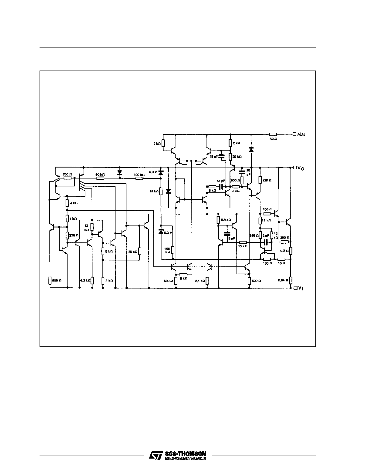
SCHEM ATIC D IAGRAM
LM137-LM237-LM337
3/14
LM137-LM237-LM337
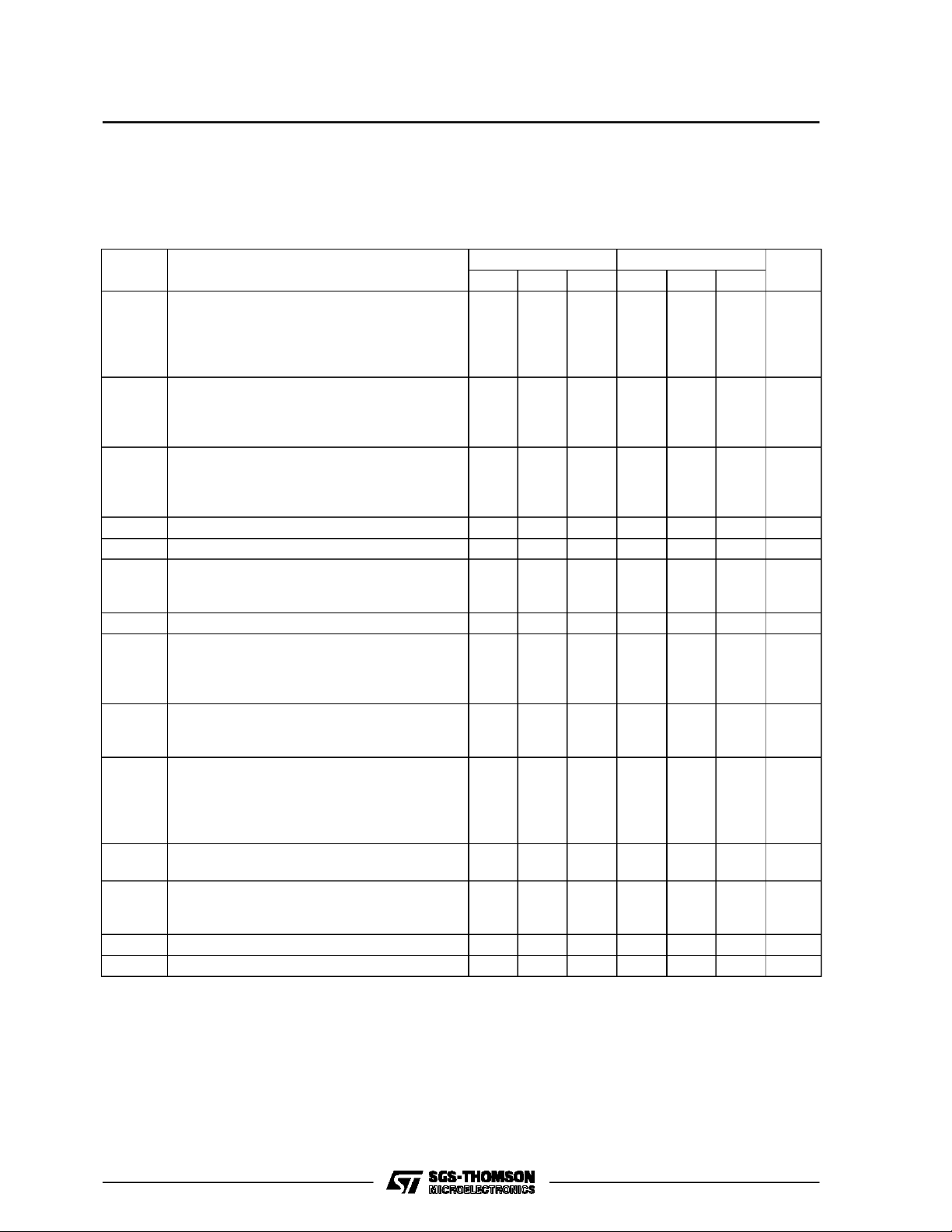
ELECTRIC AL CH A RAC TE RISI C S
LM137: -55oC<Tj<150oC
LM237: -25oC<Tj<150oC
LM337: 0oC<Tj<150oC
VI-VO=5V,IO= 0.5 A (unless ot herwis e specified)
Symbol Parameter LM137/LM237 LM337 Unit
Min. Typ. Max. Min. Typ. Max.
V
K
∆I
K
|I
O(min)
V
K
K
Notes : 1. Although power dissipation is internally limited, these specifications are applicable for power dissipation of :
Reference Voltage
ref
T
=25oC
amb
T
≤ Tj≤ T
min
3V ≤ |VI-VO|≤40V, 10mA ≤ |IO| ≤ |I
P ≤ P
K
Line Regulation
VI
(T
amb
max
O(max)
max
=25oC, 3V ≤ |VI-VO| ≤ 40V) - Note 2
|
IO= 0.1 A
IO=20mA
Load Regulation
VO
(T
=25oC, 10mA ≤ |IO| ≤ |I
amb
O(max)
|) - Note 2
|VO| ≤ 5V
|VO| ≥ 5V
Thermal Regulation (T
I
Adjustment Pin Current 65 100 65 100 µA
adj
Adjustment Pin Current Change
adj
(T
=25oC, 10mA ≤ |IO| ≤ |I
amb
=25oC, pulse 10 ms) 0.002 0.02 0.003 0.04 %/W
amb
|,
O(max)
-1.225
-1.2
-1.25
-1.275
-1.25
0.01
0.01
15
0.3
-1.3
0.02
0.02
25
0.5
-1.213
-1.2
-1.25
-1.25
0.01
0.01
15
0.3
-1.287
-1.3
0.04
0.04
50
1
25 25µA
3V ≤ |VI-VO| ≤ 40V)
Line Regulation (3V ≤ |VI-VO| ≤ 40V) - Note 2 0.02 0.05 0.02 0.07 %/V
K
VI
Load Regulation
VO
(10mA ≤ |IO| ≤ |I
|VO| ≤ 5V
|VO| ≥ 5V
O(max)
|) - Note 2
20
0.3
50
20
1
0.3701.5
| Minimum Load Current
|VI-VO| ≤ 40V
|VI-VO| ≤ 10V
I
Short Circuit Output Current
OS
|VI-VO| ≤ 15V (TO-3 and TO-220)
|VI-VO| ≤ 15V (TO-39)
|VI-VO| = 40V, Tj=25oC (TO-3 and TO-220)
|VI-VO| = 40V, Tj=25oC (TO-39)
RMS Output Noise (% of VO)
NO
T
=25oC, 10Hz ≤ f ≤ 10KHz
amb
R
Ripple Rejection Ratio
vf
1.5
0.5
0.24
0.15
VO= - 10 V, f = 120 Hz
C
=10µF66
adj
Temperature Stability 0.6 0.6 %
VT
Long Term Stability (T
VH
• 2W for TO-39
• 15W for TO-220
• 20W for TO-3 Package
I
is :
O(max)
• 1.5A for TO-3 and TO-220
• 0.5A for TO-39
2. Regulation is measured at constant junction temperature, using pulse testing with a low duty cycle. Changes in output voltage due to heating effects are covered under the specification for thermal regulation.
= 125oC, 1000H) 0.3 1 0.3 1 %
amb
2.5
1.2
2.2
5
3
1.5
2.5
1.5
2.2
10
6
0.5
0.4
0.2
0.15
0.1
0.4
0.2
0.003 0.003 %
60
77 66
60
77
V
%/V
%/V
mV
%
mV
%
mA
mA
A
A
A
A
dB
dB
4/14
LM137-LM237-LM337
5/14

LM137-LM237-LM337
6/14

THERMA L REG ULA TI ON
When power is dissipated in an IC, a temperature
gradient occurs across the IC chip affecting the individual IC circuitcomponents. WithanIC regulator,
this gradient can be especially severe since power
dissipation is large.
Thermal regulation is the effect of these temperature gradients on outputvoltage (in percentage output change)per wattof power change ina specified
time. Thermal regulation error is independent of
electrical regulation or temperature coefficient, and
occurswithin5ms to50ms after a change inpower
dissipation. Thermal regulation depends on IC
layoutaswellaselectricaldesign. Thethermalregulation of a voltage regulator is defined as the per-
The LM137 specification is 0.02 %/W max.Infigure
1,atypicalLM337’s outputdriftsonly3mVfor0.03%
of VO= – 10V) when a 10W pulse is applied for
10ms.This performance is thuswell inside thespecificationlimitof0.02%/Wx10W=0.2%max.When
the10Wpulse isendedthethermal regulation again
shows a 3mV step as the LM137 chip cools off.
Note that the load regulation error of about
8mV(0.08%) is additional to the thermal regulation
error.
In figure 2, when the 10W pulse is applied for
100ms,theoutputdrifts onlyslightly beyondthe drift
in the first 10ms and the thermal error stays well
within 0.1% (10mV).
centage changeofVO, perwatt,withinthe first10ms
aftera stepof power, is applied.
Figur e 1 . Figu re 2.
LM137-LM237-LM337
LM 337, V0= – 10V
VI–V0=– 40V
IL=0A →0.25A → 0A
Vertical sensitivity 5mV/div.
LM 337, V0= – 10V
VI–V0= – 40V
IL=0A →0.25A → 0A
Horizontal sensitivity 20msN/div.
7/14

LM137-LM237-LM337
TYPICAL AP PLICA TIONS
ADJUSTABLE NEGATIVE VOLTAGE REGULATOR
*
C1 = 1µF solidtantalum or 10µF aluminiumelectrolytic required for stability.
**
C2= 1µF solidtantalum is required only if regulator is morethan 10cm from power supplyfilter capacitor.
ADJUSTABLE LAB VOLTAGE REGULATOR
*
The10µF capacitors are optimal to improve ripplerejection.
8/14

CURRENTREGULATOR
NEGATIVE REGULATOR WITH PROTECTIONDIODES
LM137-LM237-LM337
*
WhenCLislarger than 20µF,D1 protects the LM137 in case the input supplyis shorted.
**
When C2 is larger than 10µF andV0islarger than – 25V,D2 protects the LM137in casethe outputis shorted.
9/14

LM137-LM237-LM337
* – 5.2V REGULATOR WITH ELECTRONIC SHUTDOWN
*
Minimumoutput ≡ – 1.3Vwhen control inputis low.
ADJUSTABLECURRENT REGULATOR
10/14

TO-3 MECHANICAL DATA
LM137-LM237-LM337
DIM.
mm inch
MIN. TYP. MAX. MIN. TYP. MAX.
A 11.00 13.10 0.433 0.516
B 0.97 1.15 0.038 0.045
C 1.50 1.65 0.059 0.065
D 8.32 8.92 0.327 0.351
E 19.00 20.00 0.748 0.787
G 10.70 11.10 0.421 0.437
N 16.50 17.20 0.649 0.677
P 25.00 26.00 0.984 1.023
R 4.00 4.09 0.157 0.161
U 38.50 39.30 1.515 1.547
V 30.00 30.30 1.187 1.193
P
G
U
V
N
O
R
B
A
D
C
E
P003F
11/14

LM137-LM237-LM337
TO-220 MECHANICAL DATA
DIM.
mm inch
MIN. TYP. MAX. MIN. TYP. MAX.
A 4.40 4.60 0.173 0.181
C 1.23 1.32 0.048 0.051
D 2.40 2.72 0.094 0.107
D1 1.27 0.050
E 0.49 0.70 0.019 0.027
F 0.61 0.88 0.024 0.034
F1 1.14 1.70 0.044 0.067
F2 1.14 1.70 0.044 0.067
G 4.95 5.15 0.194 0.203
G1 2.4 2.7 0.094 0.106
H2 10.0 10.40 0.393 0.409
L2 16.4 0.645
L4 13.0 14.0 0.511 0.551
L5 2.65 2.95 0.104 0.116
L6 15.2 15.9 0.598 0.625
L7 6.2 6.6 0.244 0.260
L9 3.5 4.2 0.137 0.165
DIA. 3.75 3.85 0.147 0.151
E
A
L4
D
F2
F1
G1
H2
G
F
C
D1
L2
Dia.
L5
L7
L6
L9
P011C
12/14

TO39 MECHANICAL DATA
LM137-LM237-LM337
DIM.
mm inch
MIN. TYP. MAX. MIN. TYP. MAX.
A 12.7 0.500
B 0.49 0.019
D 6.6 0.260
E 8.5 0.334
F 9.4 0.370
G 5.08 0.200
H 1.2 0.047
I 0.9 0.035
o
L45
(typ.)
I
H
G
F
L
DA
E
B
P008B
13/14

LM137-LM237-LM337
Information furnished is believed to be accurate and reliable. However, SGS-THOMSON Microelectronics assumes no responsability for the
consequences of use of such information nor for any infringement of patents or other rights of third parties which may results from its use. No
license isgranted by implication or otherwise underany patent or patent rights of SGS-THOMSON Microelectronics. Specificationsmentioned
in this publication are subject to change without notice. This publication supersedes and replaces all information previously supplied.
SGS-THOMSON Microelectronicsproductsare not authorized foruse ascritical componentsin life support devices or systemswithout express
written approval of SGS-THOMSON Microelectonics.
1994 SGS-THOMSON Microelectronics- All Rights Reserved
Australia - Brazil - France - Germany - Hong Kong - Italy - Japan - Korea - Malaysia - Malta - Morocco - The Netherlands -
Singapore - Spain - Sweden- Switzerland - Taiwan - Thailand - UnitedKingdom - U.S.A
SGS-THOMSON Microelectronics GROUP OF COMPANIES
14/14
 Loading...