

Datasheet LM311D, LM311, LM211N, LM211D, LM211 Datasheet (SGS Thomson Microelectronics)
...
.MAXIMUM INPUT CURRENT : 150nA
.MAXIMUM OFFSETCURRENT : 20nA
.DIFFERENTIAL INPUT VOLTAGE RANGE :
±30V
.POWERCONSUMPTION: 135mW AT±15V
.SUPPLYVOLTAGE: +5V TO ±15V
.OUTPUTCURRENT : 50mA
LM111
LM211 - LM311
VOLTAGE COMPARATORS
DESCRIPTION
The LM111, LM211 and LM311 are voltage
comparatorsthathavelowinputcurrents.
Theyarealsodesignedtooperateoverawiderange
of supplyvoltages: fromstandard±15V operational
amplifier supplies down to the single +5V supply
used for IClogic.
TheiroutputiscompatiblewithRTL-DTLandTTLas
wellas MOScircuitsand can switch voltages up to
+50Vat outputcurrentsas high as 50mA.
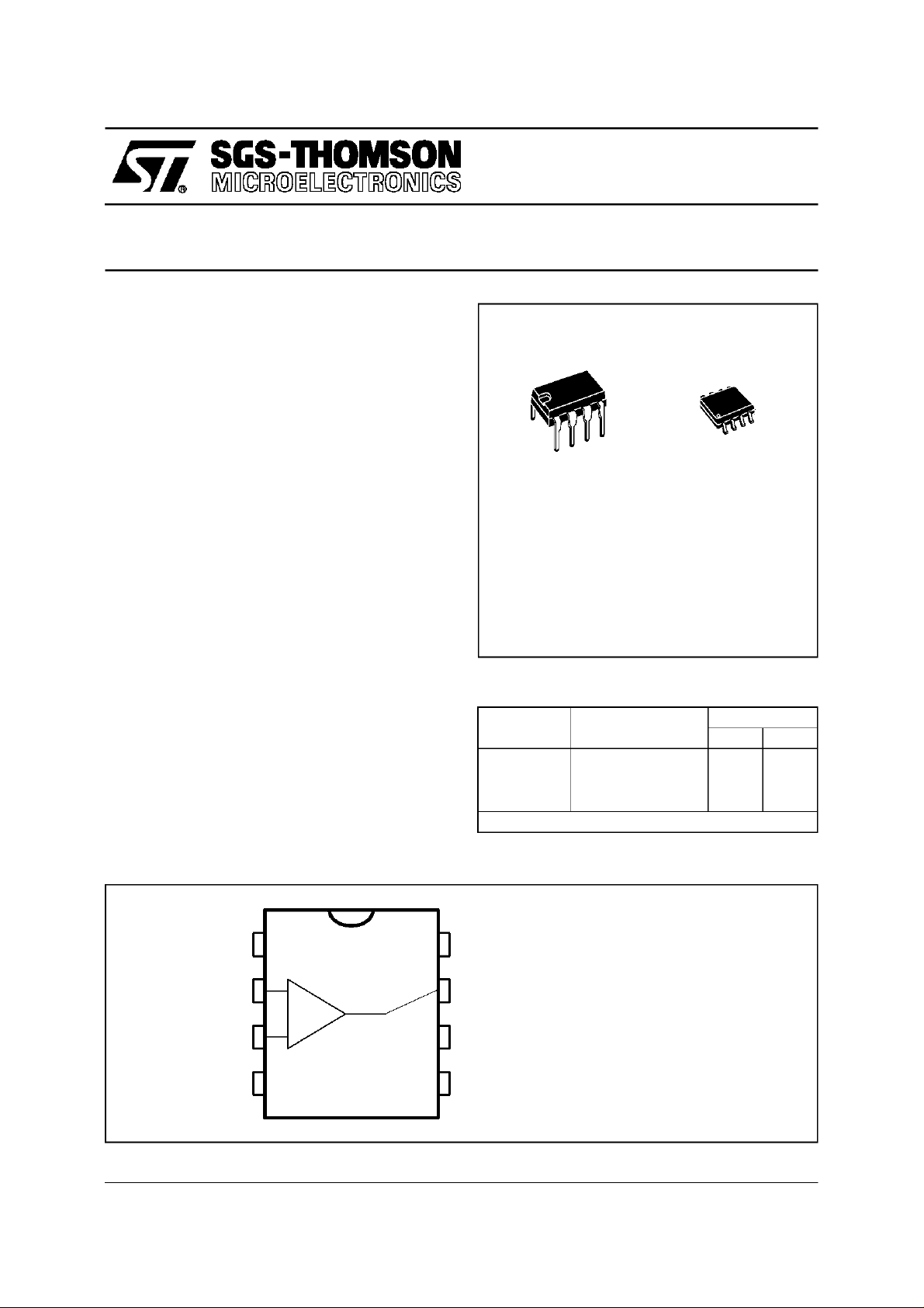
PIN CONNECTIONS (top view)
1
2
3
+
-
N
DIP8
(Plastic Package)
ORDER CODES
CC
CC
-
+
Temperature
Part Number
LM111 –55, 125
LM211 –40, 105
LM311 0, 70
Example : LM311D
8
7
6
1 - Ground
2 - Non-inverting input
3 - Inverting input
4-V
5 - Balance
6 - Strobe/balance
7 - Output
8-V
D
SO8
(Plastic Micropackage)
Package
Range
o
C ••
o
C ••
o
C ••
ND
October1997
4
5
1/9
LM111 - LM2 11 - LM311
SCHEMATIC DIAGRAM
Strobe/balance
Non-inverting
input
Inverting
input
300
Q5
Q1
R3
Ω
R1
1.3k
D1
5V
Balance
R4
Ω
300
R8
Q9
Q22
Ω
Q10
600
R17
60
R15
450
R14
2k
R9
Ω
Q20
Q11
Q19
R16
400
Q18
Ω
R10
4k
Ω
Q14
Ω
Ω
Q17
Ω
Q16
Q6
R2
Ω
1.3k
Ω
1.2k
Q3
D2
5V
Q2
250
R6
R19
Ω
Ω
Q4
Q23
R5
70
R7
1.2k
Ω
Q7
Ω
R18
200
750
Q8
Q21
Ω
Q13
Collector o u tput
V
CC
Q12
R11
Ω
130
R12
Ω
600
V
CC
Q15
R13
4
Ω
Emitter output or ground
ABSOLUTE MAXIMUM RATINGS
Symbol Parameter LM111 LM211 LM311 Unit
V
CC
V
id
V
i
P
tot
T
oper
T
stg
V
(1–4)
V
(7–4)
Outputshort-circuitduration : 10s LM111: +150oC
Voltage atstrobe pin : V
Note : 1. This rating applies for ±15V supplies. The positive input voltage limit is30V above the negative. Thenegativeinput voltagelimit is
2/9
Supply Voltage 36 36 36 V
Differential Input Voltage ±30 ±30 ±30 V
Input Voltage – (note 1) ±15 ±15 ±15 V
Power Dissipation 500 mW
Operating Free-air Temperature Range –55 to +125 –40 to +105 0 to +70
Storage Temperature Range –65 to +150 –65 to +150 –65 to +150
Ground to Negative Supply Voltage 30 30 30 V
Output to Negative Supply Voltage 50 50 40 V
+
–5V Maximum junction temperature LM211 : +150oC
CC
equal to the negative supply voltageor 30V below thepositive supply, whichever is less.
LM311: +150
o
C
o
C
o
C
LM111 - LM211 - LM311
ELECTRICAL CHARACTERISTICS
= ±15V, T
V
CC
Symbol Parameter
Input Offset Voltage (RS≤ 50kΩ) – (note 1)
V
io
Input Offset Current – (note 1)
I
io
Input Bias Current – (note 1)
I
ib
Large Signal Voltage Gain 40 200 40 200 V/mV
A
vd
Supply Currents
+
I
CC
-
I
CC
Input Common Mode Voltage Range
V
icm
V
Low Level Output Voltage
OL
High Level Output Current
I
OH
I
Notes: 1. The offset voltage,offset current and bias current specificationsapply for any supply voltage froma single+5V supply up to ±15V
Strobe Current 3 3 mA
strobe
Response Time – (note 2) 200 200 ns
t
re
supplies.
The offset voltages and offset currents given are the maximumvalues requiredto drive the outputdown to +1V or upto +14V with
a 1mA load current. Thus,these parameters define an errorband and take into accountthe worst-case of voltagegain and input
impedance.
2. The response time specified(see definitions) is for a 100mV input step with5mV overdrive.
=25oC(unless otherwise specified)
amb
= +25oC
T
amb
. ≤ T
T
min
T
amb
. ≤ T
T
min
T
amb
. ≤ T
T
min
amb
= +25oC
amb
= +25oC
amb
≤ T
≤ T
≤ T
max
max
max
.
.
.
Positive
Negative
. ≤ T
T
min
T
amb
T
min.
+
≥ +4.5 V, V
V
CC
= 8mA V
I
o
T
amb
. ≤ T
T
min
≤ T
amb
= +25oC, IO= 50mA V
≤ T
amb
= +25oCV
amb
. -14.5 +13.8
max
-5mV
i ≤
-10mV
V
≤ T
.
max
-
CC
≤ T
.V
max
=0
i ≤
-6mV
i ≤
-10mV
V
i ≤
≥+ 5mV, VO= +35V
i
≥ +10mV, VO=+5V
V
i
≥+ 5mV, VO= +35V
i
LM111 - LM211 LM311
Min. Typ. Max. Min. Typ. Max.
0.7 3
4
410
20
60 100
150
5.1
4.1
6
5
+13
-14.7
0.75
0.23
1.5
0.4
-14.5
2 7.5
10
650
70
100 250
300
5.1
7.5
4.1
+13.8
5
+13
-14.7
0.75
0.23
1.5
0.4
0.2
0.2 50nAnA
0.1100.5
Unit
mV
nA
nA
mA
µA
V
V
3/9

LM111 - LM211 - LM311
TRANSFERT CHARACTERISTICS
60
Normal output
50
Emitter follower
output
40
RL=600
30
20
OUTPUT VOLTAGE (V)
10
0
-1 -5 0 0.5 1
Ω
RL=1k
VL = +50 V
T
=+25 C
amb
VCC=+30 V
DIFFERENTIA L INPUT VOLTA GE (mV)
+
V
CC
-0.5
-1.5
-1
CO MMON MODE L IMITS
Ω
OUTPUT LIMI TING CHARACTERISTICS
140
120
100
80
60
40
20
SHORT-CIRCUIT CURRENT (mA)
0
0 5 10 15
T
= +25 C
am b
n
o
ti
a
p
i
s
s
i
d
r
we
o
P
Sh o rt c ircuit c urre nt
OUT P UT VOLTAG E (V)
INPUT O FF S ET CUR RE NT
30
VCC= –15V
20
Raised
0.7
POWER DISSIPATION (W)
0.6
0.5
0.4
0.3
0.2
0.1
0
0.4
0.2
COMMON MODE LIMITS (V)
-
V
CC
01020304050607080
TE MPE RATUR E( C)
INPUT BIAS CURRENT (nA)
10
INPUT OFFSET CURRENT ( nA)
0
-55 -35 -15 5 25 45 65 85 105 125
INP UT BIAS CUR RE NT
400
300
200
100
0
-55 -35 -15 5 25 45 65 85 105 125
Raised
Norma l
VCC= –15V
TEMP ERATURE ( C)
Norma l
TE MPE RATURE( C)
4/9

LM111 - LM211 - LM311
EQUIVALENT INPUT OFFSET ERROR
100
LM111
LM211
T
=+25 C
amb
10
EQUIVALENTINPUT
OFFSET VOLTAGE (mV)
1
Maximum
Typica l
VIO=VIO+RSI
ID
0.1
10k 100k 1M 10M
INPUT RESISTANCE (Ω)
LOW LEVEL OUTPUT SATURATION VOLTAGE
0.8
LM111
0.7
0.6
0.5
0.4
LM211 › T
T
=-55 C
amb
amb
= +125 C
EQUIV A L ENT INPUT OFFSET ERROR
100
T
=+25 C
amb
LM 311
Maximum
10
Typical
EQUIVALENTINPUT
OFFSET VOLTAGE (mV)
VIO=VIO+RS I
ID
10k 100k 1M 10M
INPUT RESISTANCE (Ω)
LOW LEVEL O UTPU T S ATURATION VOLTAGE
0.8
LM311 T
0.7
0.6
0.5
0.4
amb
= +25 C
0.3
0.2
T
= +25 C
0.1
SATURATION VOLTAGE (V)
0
01020304050
amb
OUTP UT C URE NT (m A)
180
160
140
120
100
80
60
40
20
INPUT BIAS CURRENT (nA)
0.3
0.2
0.1
SATURATION VOLTAGE (V)
0
01020304050
O UTPU T C URRE NT (mA)
INPUT C HARACTE RISTICS
VCC= –15V
T
=+25 C
amb
0
-16 -12 -8 -4 0 4 8 12 16
DIFFERENTIALINPUT VOLTAGE (V)
5/9

LM111 - LM211 - LM311
INPUT VOLTAGE (mV)
OUTPUT VOLTAGE (V)
INPUT VOLTAGE (mV)
RESPONSE TIME FOR VARIOUS
INPUT OVERDRIVES
5
20mV
4
5mV
3
2
2mV
VCC = –15V
T
1
0
100
V
-
I
+
50
0
0 0.2 0.4 0.6 0.8
TIME (µs)
RESPONSE TIME FOR VARIOUS
INPUT OVERDRIVES
15
OUTPUT VOLTAGE (V)
10
-5
-10
-15
100
50
5
0
20mV
5mV
2mV
0
V
I
VCC = –15V
T
amb
amb
+5 V
+
-
=+25 C
500
VCC+
VCC-
=+25
RESPONSE TIM E FOR VARIOUS
INPUT OVERDRIVES
5
4
20mV
3
2
5mV
1
-50
OUTPUT VOLTAGE (V)
2mV
0
Ω
V
o
INPUT VOLTAGE (mV)
-100
0 0.2 0.4 0.6 0.8
+5 V
V
-
I
+
VCC = –15V
T
=+25 C
amb
500
V
Ω
o
TIME (µs)
RESPONSE TIME FOR VARIOUS
INPUT OVERDRIVES
20mV
15
10
5mV
V
o
Ω
2k
5
2mV
0
-5
-10
-15
0
OUTPUT VOLTAGE (V)
INPUT VOLTAGE (mV)
-50
C
-100
VCC+
V
+
I
-
VCC-
VCC = –15V
T
=+25
amb
V
o
Ω
2k
C
6/9
01234
TIM E (µs)
01234
TIM E (µs)

TYPICAL APPLICATIONS
CRYSTALOSCILLATOR
=+5V
V
2
3
CC
Ω
100kHz C 2
8
LM111
4
1
R2
100k
R1
100k
Ω
C1
0.1µF
7
2k
R4
Ω
50k
10pF
R3
Ω
Output
LM111 - LM211 - LM311
LOW VOLTAGE ADJUSTABLE REFERENCE
SUPPLY
=+5V
V
2N 2222
3.9k
2N 1304
R2
1k
3
2
CC
Ω
8
LM111
4
R1
Ω
10k
R3
R4
Ω
500
Ω
7
1
Output
+C1*
µ
1.5
F
*Sold tantalum
100KHz FREE RUNNING MULTIVIBRATOR
=+5V
V
C1
1200pF
R2
20k
Ω
R1
20k
Ω
3
2
CC
R3
10k
LM111
4
*TTLor DTLfan-out two
R5
Ω
1k
Ω
8
7
R4
39k
Ω
Squa re wave output
1
AUXILIARY CIRCUITS
2
LM111
3
2N 2222
STROBE
6
Q1
1k
R1
7
TTL strobe
Ω
INCREASING INPUT STAGE
CURRENT
5
2
6
LM111
3
TTL INTERFACE WITH HIGH LEVEL LOGIC
=+5V
V
Input
47k
R2
R3
Ω
82k
2
3
Ω
R4
Ω
82k
8
LM111
4
R1
Ω
240k
C1
CC
7
1
To TTLlogic
0 to +30Vs wing and
+15Vthresholg
R5
1k
OFFSETBALANCING
R2
Ω
3k
V
CC
8
7
5k
Ω
5
6
2
LM111
8
7
3
Ω
V
CC
7/9

LM111 - LM2 11 - LM311
PACKAGE MECANICAL DATA
8 PINS- PLASTICDIP
Dim.
A 3.32 0.131
a1 0.51 0.020
B 1.15 1.65 0.045 0.065
b 0.356 0.55 0.014 0.022
b1 0.204 0.304 0.008 0.012
D 10.92 0.430
E 7.95 9.75 0.313 0.384
e 2.54 0.100
e3 7.62 0.300
e4 7.62 0.300
F 6.6 0260
i 5.08 0.200
L 3.18 3.81 0.125 0.150
Z 1.52 0.060
Min. Typ. Max. Min. Typ. Max.
Millimeters Inches
DIP8.TBL PM-DIP8.EPS
8/9

PACKAGE MECANICAL DATA
8 PINS- PLASTICMICROPACKAGE(SO)
LM111 - LM211 - LM311
Dim.
Min. Typ. Max. Min. Typ. Max.
Millimeters Inches
A 1.75 0.069
a1 0.1 0.25 0.004 0.010
a2 1.65 0.065
a3 0.65 0.85 0.026 0.033
b 0.35 0.48 0.014 0.019
b1 0.19 0.25 0.007 0.010
C 0.25 0.5 0.010 0.020
c1 45
o
(typ.)
D 4.8 5.0 0.189 0.197
E 5.8 6.2 0.228 0.244
e 1.27 0.050
e3 3.81 0.150
F 3.8 4.0 0.150 0.157
L 0.4 1.27 0.016 0.050
M 0.6 0.024
S8
Information furnished is believed to be accurate and reliable. However, SGS-THOMSON Microelectronics assumes no responsibility for the consequences of use of such information nor for any infringement of patents or other rights of third parties which
may result from its use. No license is granted by implication or otherwise under any patent or patent rights of SGS-THOMSON
Microelectronics. Specifications mentioned in this publicationare subject to change without notice. This publication supersedes
and replaces all information previously supplied. SGS-THOMSON Microelectronics products are not authorized for use as critical
components in life support devices or systems without express written approval of SGS-THOMSON Microelectronics.
o
(max.)
PM-SO8.EPS
SO8.TBL
1997 SGS-THOMSON Microelectronics – Printed in Italy – All Rights Reserved
SGS-THOMSON Microelectronics GROUP OF COMPANIES
Australia - Brazil- Canada - China - France - Germany - Hong Kong - Italy - Japan - Korea - Malaysia - Malta - Morocco
The Netherlands - Singapore - Spain - Sweden - Switzerland - Taiwan - Thailand - United Kingdom- U.S.A.
ORDERCODE :
9/9
 Loading...