

LOW POWER DUAL OPERATIONAL AMPLIFIERS
.INTERNALLYFREQUENCYCOMPENSATED
.LARGEDC VOLTAGEGAIN: 100dB
.WIDEBANDWIDTH (unitygain): 1.1MHz
(temperaturecompensated)
.VERY LOW SUPPLY CURRENT/OP (500µA) -
ESSENTIALLY INDEPENDENT OF SUPPLY
VOLTAGE
.LOW INPUTBIAS CURRENT : 20nA
(temperaturecompensated)
.LOW INPUTOFFSETCURRENT :2nA
.INPUT COMMON-MODE VOLTAGE RANGE
INCLUDES GROUND
.DIFFERENTIAL INPUT VOLTAGE RANGE
EQUALTO THE POWER SUPPLYVOLTAGE
.LARGE OUTPUT VOLTAGE SWING 0V TO
(V
–1.5V)
CC
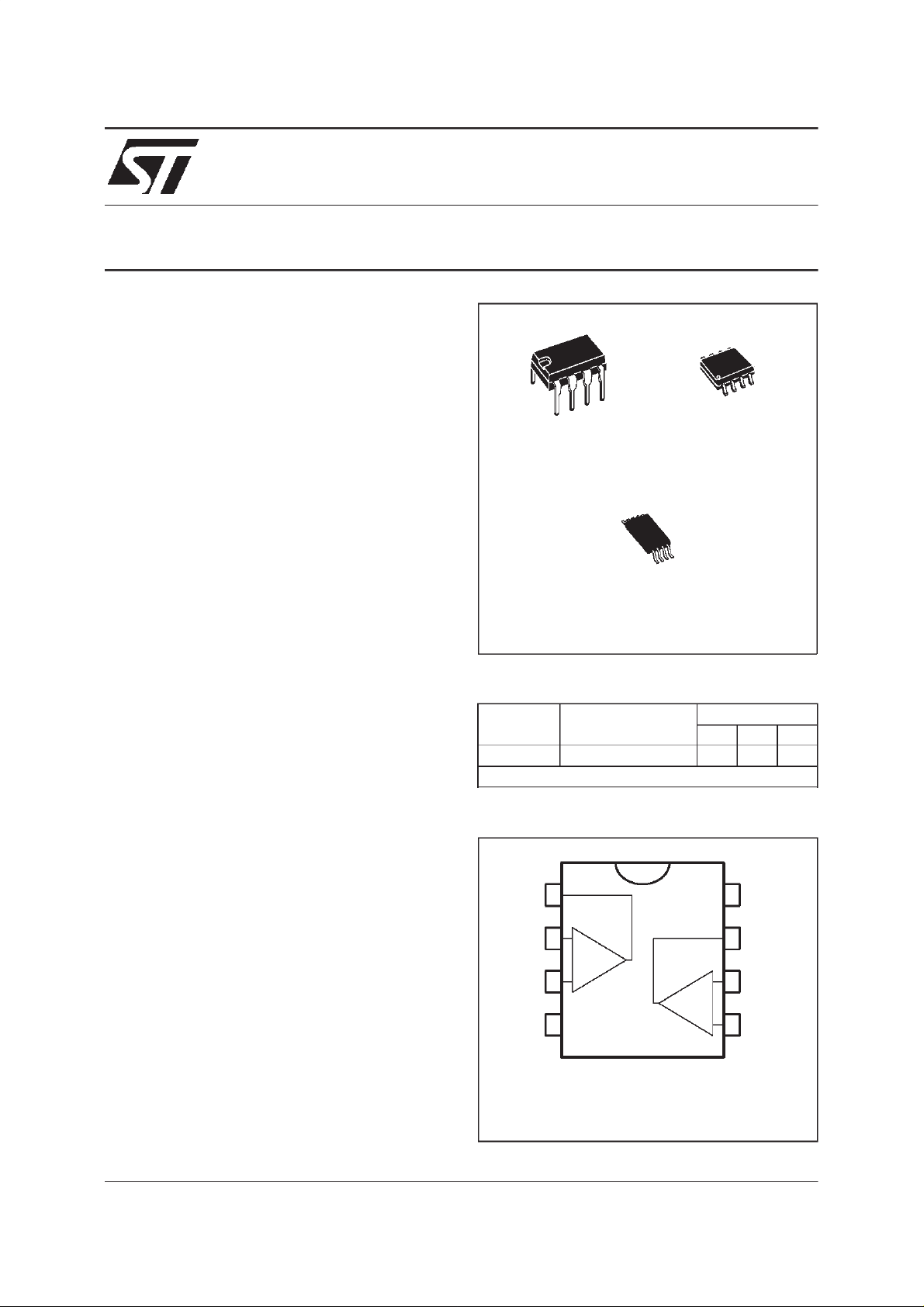
N
DIP8
(PlasticPackage)
(Thin ShrinkSmallOutline Package)
(PlasticMicropackage)
P
TSSOP8
LM2904
D
SO8
DESCRIP TION
Thiscircuit consistsof twoindependent,high gain,
internally frequency compensated which were
designed specificallyfor automotiveand industrial
controlsystem.It operatesfrom asinglepowersupply over a wide range of voltages. The low power
supplydrainisindependentof the magnitudeof the
powersupplyvoltage.
Applicationareas include transduceramplifiers, dc
gainblocksandalltheconventionalop-ampcircuits
whichnowcanbemoreeasilyimplementedinsingle
powersupply systems.Forexample,thesecircuits
can bedirectlysuppliedwith off the standard + 5V
whichisusedinlogicsystemsandwilleasilyprovide
the required interfaceelectronicswithout requiring
any additionalpowersupply.
In thelinearmodethe input common-modevoltage
range includesground and the output voltage can
also swing to ground, even though operated from
only a single powersupply voltage.
ORDER CODES
Part
Number
LM2904 -40
Example : LM2904D
PIN CONNECTIONS (top view)
1
2
3
45
1 -Output 1
2 -Inverting input 1
3 -Non-inverting input1
-
4-V
CC
Temperature
Range
o
C, +125oC •••
-
+
5 - Non-inverting input 2
6 - Invertinginput 2
7 - Ouput2
8-V
CC
Package
NDP
8
7
-
+
+
6
January 1999
1/12
LM2904
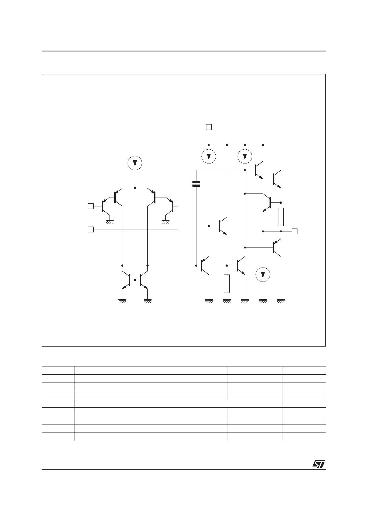
SCHEMATIC DIAGRAM ( 1/2 LM2904)
V
CC
Inverting
input
Non-inverting
input
6µA
Q2
Q3
Q8 Q9
µ
4
A
100
µ
A
Q5
C
C
Q4Q1
Q7
Q11
Q6
R
SC
Output
Q13
Q10
Q12
50
µ
A
GND
ABSOLUTE MAXIMUM RATINGS
Symbol Parameter LM2904 Unit
Supply Voltage +32 V
Input Voltage –0.3 to +32 V
i
Differential Input Voltage +32 V
Output Short-circuit Duration - (note 2)
Power Dissipation 500 mW
Input Current - (note 1) 50 mA
Operating Free-air Temperature Range -40 to +125
Storage Temperature Range –65 to +150
2/12
V
CC
V
V
id
P
tot
I
in
T
oper
T
stg
o
C
o
C
LM2904
ELECTRICAL CHARACTERISTICS
+
= +5V, V
V
CC
Symbol Parameter Min. Typ. Max. Unit
V
io
I
io
I
ib
A
vd
SVR Supply Voltage Rejection Ratio (R
I
CC
V
icm
CMR Common-mode Rejection Ratio (R
I
source
I
sink
V
OPP
V
OH
V
OL
SR Slew Rate (V
GBP Gain Bandwidth Product
THD Total Harmonic Distortion
–
= Ground, VO= 1.4V, T
CC
=25oC (unless otherwise specified)
amb
Input OffsetVoltage - (note 3)
T
T
amb
min.
=25oC
≤ T
amb
≤ T
max
.
27
Input OffsetCurrent
T
T
amb
min.
=25oC
≤ T
amb
≤ T
max
.
230
Input Bias Current - (note 4)
T
T
amb
min.
=25oC
≤ T
amb
≤ T
max
.
20 150
Large Signal Voltage Gain
= +15V, RL=2kΩ,VO= 1.4V to 11.4V)
(V
(V
CC
CC
=25oC
T
amb
≤ T
T
min.
+
= 5 to 30V)
=25oC
T
amb
≤ T
T
min.
amb
amb
≤ T
≤ T
max
max
.
= 10kΩ)
S
.
50
25
65
65
100
100
Supply Current, allAmp, no Load
V
CC
V
CC
= +5V, T
= +30V, T
min.
min.
≤ T
≤ T
amb
amb
≤ T
≤ T
max
max
.
.
0.7 1.2
Input Common Mode Voltage Range
= +30V) - (note 6)
(V
CC
T
T
T
T
amb
min
amb
min.
=25oC
. ≤ T
=25oC
≤ T
amb
amb
≤ T
≤ T
max
max
.
= 10kΩ)
S
.
70
60
0
0
85
Output Source Current
= +15V, Vo= 2V, Vid= +1V) 20 40 60
(V
CC
Output Current Sink (Vid= -1V)
= +15V, VO=2V
V
CC
= +15V, VO= +0.2V
V
CC
10
12
20
50
Output Voltage Swing (RL=2kΩ)
26
26
27
27
0
0
27
28
=25oC
T
amb
≤ T
≤ T
T
min.
amb
max
.
High Level Output Voltage (V
=25oCR
T
amb
T
T
T
min
amb
min.
. ≤ T
≤ T
≤ T
max
max
.
.
amb
=25oCR
≤ T
amb
+
= 30V)
CC
=2kΩ
L
= 10kΩ
L
Low Level Output Voltage(RL= 10kΩ)
=25oC
T
amb
. ≤ T
T
min
100pF, unity gain) 0.3 0.6
= 30V, f = 100kHz,
(V
CC
= 10mV, RL=2kΩ,CL= 100pF) 0.7 1.1
V
in
(f = 1kHz, A
= 100pF, VO=2PP)
C
L
≤ T
amb
max.
= 15V, VI= 0.5 to 3V, RL=2kΩ,CL=
CC
= 20dB, RL=2kΩ,VCC= 30V,
v
520
0.02
9
40
200
2
+
V
–1.5
CC
+
–2
V
CC
+
V
–1.5
CC
+
–2
V
CC
20
mV
nA
nA
V/mV
dB
mA
V
dB
mA
mA
µA
V
V
mV
V/µs
MHz
%
3/12

LM2904
ELECTRICAL CHARACTERISTICS (continued)
Symbol Parameter Min. Typ. Max Unit
DV
DI
V
O1/VO2
Notes : 1. This input current only exist when the voltage at any of the input leads is driven negative. It is due to the collec-
OPEN LOOP FREQUENCY RESPONSE
Input Offset Voltage Drift 7 30 µA/oC
io
Input Offset Current Drift 10 300 pA/oC
io
Channel Separation (note 5)
1kHz ≤ f ≤ 20kHz 120
tor-base junction of the input PNP transistor becoming forward biased and thereby acting as input diode clamps.
In addition to this diode action, there is also NPN parasitic action on the IC chip. This transistor action can cause
the output voltages of the Op-amps to go to the V
duration that an input is driven negative.
This is not destructive and normal output will set up again for input voltage higher than –0.3V.
2. Short-circuits from the output to V
approximatively 40mA independent of the magnitude of V
short-circuits on all amplifiers.
= 1.4V, RS=0Ω,5V<V
3. V
O
CC
can cause excessive heating if V
CC
+
< 30V, 0 < Vic< V
4. The direction of the input current is out of the IC. This current is essentially constant, independent of the state of
the output so no loading change exists on the input lines.
5. Due to the proximity of external components insure that coupling is not originating via stray capacitance between
these external parts. This typically can be detected as this type of capacitance increases at higher frequences.
6. The input common-mode voltage of either input signal voltage should not be allowed to go negative by more than
0.3V. The upper end of the common-mode voltage range is V
But either or both inputs can go to +32V without damage.
(NOTE 3)
140
120
100
0.1µF
V
I
VCC/2
80
VCC= 30V &
60
-55 C
T
-
+
amb
10M
Ω
V
CC
+125 C
V
O
voltage level (or to ground for a large overdrive) for the time
CC
+
> 15V. The maximum output current is
+
– 1.5V.
CC
CC
. Destructive dissipation can result from simultaneous
CC
+
– 1.5V.
CC
LARGE SIGNALFREQUENCYRES PONSE
20
Ω
1k
15
V
I
+7V
10
Ω
100k
+15V
-
+
VO
Ω
2k
dB
40
VOLTAGE GAIN (dB)
20
VCC=+10to+15V&
T
amb
+125 C
-55 C
0
1.0 10 100 1k 10k 100k 1M 10M
FREQUENCY(Hz)
VOLAGE FOLLOWER PULSE RESPONSE
4
3
RL 2 k
VCC = +15V
2
OUTPUT
1
VOLTAGE (V)
0
3
2
1
INPUT
010203040
VOLTAGE (V)
TIME (µs)
Ω
5
OUTPUT SWING (Vpp)
0
1k 10k 100k 1M
FREQUENCY (Hz)
OUTPUT CHARACTERISTICS
10
1
0.1
OUTPUT VOLTAGE (V)
0.01
0,001 0,01 0,1 1 10 100
VCC = +5V
VCC = +15V
VCC = +30V
vcc/2
T
-
+
amb
v
cc
OUTPUT SINK CURRENT (mA)
=+25 C
I
O
V
O
4/12

LM2904
VOLTA GE FOLLOWER PULSSE RESPONSE
(SMAL L SIGNAL)
500
e
l
+
-
Output
e
O
50pF
Input
T
amb
VCC=30V
=+25
C
450
400
350
OUTPUT VOLTAGE (mV)
300
250
012345678
TIM E (µs)
INPUT CURRENT (Note 1)
90
80
VI=0V
70
60
VCC=+30V
50
40
VCC=+15V
30
20
INPUT CURRENT (mA)
VCC=+5V
10
0
-55 -35 -15 5 25 45 65 85 105 125
TEMPERATURE( C)
INPUT VOLTAGE RANGE
15
10
NØga tive
5
P os itive
INPUT VOLTAGE (V)
0 5 10 15
PO WER SUPP LY VOLTAGE (–V)
OUTPUT CHARACTERISTICS
8
7
VCC/2
6
(V)
5
+
CC
4
TO V
Indepe nd ent of V
3
2
OUTPUT VOLTAGE REFERENCED
1
0,01 0,1 1 10 100
0,001
T
amb
+
-
=+25 C
V
CC
V
O
I
O
CC
OUTPUT SOURCE CURRENT (mA)
CURRENT LI MITI NG (Note 1)
90
80
-
I
O
70
60
+
50
40
30
20
OUTPUT CURRENT (mA)
10
0
-55 -35 -15 5 25 45 65 85 105 125
TEMPERATURE( C)
SUPPLY CURRENT
4
V
CC
I
3
mA
2
D
-
+
T
= 0 C to +125 C
amb
1
SUPPLY CURRENT (mA)
T
=-55 C
amb
0102030
PO SITIVE S UPP LY VOLTAGE (V)
5/12

LM2904
160
R=20k
L
Ω
120
80
R=2k
L
Ω
40
VOLTAGE GAIN (dB)
010203040
POSITIVE SUPP LYVOLTAGE (V)
160
R = 20k
L
Ω
120
80
R=2k
Ω
L
40
VOLTAGE GAIN (dB)
0102030
POSITIVE S UPPLY VOLTAGE (V)
100
75
50
25
INPUT CURRENT (nA)
T=+25 C
amb
0102030
P OS ITIVE S UP PLY VOLTAGE (V)
1.5
1.35
1.2
1.05
0.9
0.75
V=15V
CC
0.6
0.45
0.3
0.15
0
GAIN BANDWIDTH PRODUCT (MHz)
-55-35-15 5 25 45 65 85 105 125
TEMP ERATURE ( C)
6/12
115
110
105
100
95
90
85
80
75
70
65
-55-35-15 5 25 4565 85 105125
60
POWER SUPPLY REJECTION RATIO (dB)
TEMP ERATURE ( C)
SVR
115
110
105
100
95
90
85
80
75
70
65
-55-35-15 5 25 45 65 85 105 125
60
COMMON MODE REJECTION RATIO (dB)
TEMPERATURE ( C)

LM2904
TYPICAL APPLI CATIONS (single supply voltage) VCC=+5V
AC COUPLED INVERTING AMPLIFIER
R
f
Ω
100k
R1
C
Ω
10k
I
1/2
LM2904
R
B
Ω
e
I
R2
~
Ω
100k
V
CC
C1
µ
10
6.2k
R3
Ω
100k
F
R
f
A=-
V
R1
(as shown A = -10)
V
C
o
0
e
o
R
L
Ω
10k
2V
PP
AC COUPLED NON-INVERTING AMPLIFIE R
R1
Ω
100k
C1
0.1µF
C
I
e
R3
I
1M
~
C2
10µF
Ω
DC
R2
1M
1/2
LM2904
6.2k
100k
100k
R5
R4
Ω
R
B
Ω
Ω
V
CC
Ω
R2
A=1+
V
R1
(as shown A = 11)
V
C
o
0
e
o
R
L
Ω
10k
2V
PP
NON-INVE RTI NG DC AMP L IFIE R
=1+
A
V
Ω
10k
R1
10k
e
1/2
LM2904
R2
Ω
1M
Ω
O
+5V
(V)
O
e
0
(As s hown = 101)A
e
I
R2
R1
(mV)
DC SUMMING AMPL I FIER
e
1
V
e
2
e
3
e
4
Ω
100k
Ω
100k
Ω
100k
Ω
100k
Ω
100k
eo=e1+e2-e3-e
where(e1+e2)≥(e3+e4)
to keep e
≥ 0V
o
LM2904
4
1/2
100k
e
O
Ω
7/12

LM2904
HIGH I NPUT Z, DC DI F FE RENTIAL
AMPLIFIER
R2
Ω
R1
100k
Ω
100k
1/2
LM2904
+V1
+V2
if R1=R5andR3=R4=R6=R
2R
eo=[1+
As showne
1
] (e2− e1)
R
2
=101(e2-e1).
o
R3
100k
100k
Ω
1/2
LM2904
7
R4
USING SYMMETRICAL AMPLIFIERS T O
REDUCE INPUT C URRENT
1/2
LM2904
I
I
B
I
e
I
I
B
Ω
2N 929
0.001µF
I
3M
B
1/2
Ω
LM2904
I
B
I
1.5M
B
Ω
V
o
e
o
Input current compensation
HIGH INPUT Z ADJUSTAB L E GAI N DC
INSTRUMENTATION AMPLIFIER
R1
Ω
100k
1/2
e
1
R2
Ω
2k
e
2
LM2904
Ga in adjus t
100k
1/2
LM2904
R5
Ω
if R1=R5andR3=R4=R6=R
2R
eo=[1+
As shown e
1
] (e2− e1)
R
2
=101(e2-e1)
o
R3
100k
R6
100k
Ω
Ω
7
1/2
LM2904
R7
100k
R4
100k
Ω
Ω
LOW DRIFT PEAK DETECTOR
I
B
1/2
I
LM2904
C
2I
2N 929
B
B
0.001µF
I
B
3R
Ω
3M
I
B
Z
LM2904
1/2
LM2904
e
e
O
I
Z
I
1µF
1M
2I
B
R
Ω
e
o
1/2
Input curre nt
compens ation
o
8/12

ACTIVE BAND-PASS FILTER
R2
Ω
100k
+V1
R3
Ω
100k
Fo=1kHz
Q=50
= 100(40dB)
A
V
R1
100k
1/2
LM2904
R4
10M
LM2904
Ω
Ω
C2
330pF
1/2
R6
470k
Ω
R8
100k
Ω
C1
330pF
1/2
LM2904
10µF
C3
R5
470k
R7
100k
Ω
Ω
LM2904
V
o
V
CC
9/12

LM2904
PACKAGE MECHANIC AL DATA
8 PINS - PLASTIC DIP
Dimensions
Min. Typ. Max. Min. Typ. Max.
Millimeters Inches
A 3.32 0.131
a1 0.51 0.020
B 1.15 1.65 0.045 0.065
b 0.356 0.55 0.014 0.022
b1 0.204 0.304 0.008 0.012
D 10.92 0.430
E 7.95 9.75 0.313 0.384
e 2.54 0.100
e3 7.62 0.300
e4 7.62 0.300
F 6.6 0260
i 5.08 0.200
L 3.18 3.81 0.125 0.150
Z 1.52 0.060
PM-DIP8.EPS
DIP8.TBL
10/12

PACKAGE MECHANIC AL DATA
8 PINS - PLASTIC MICROPACKAGE (SO)
LM2904
Dimensions
Min. Typ. Max. Min. Typ. Max.
Millimeters Inches
A 1.75 0.069
a1 0.1 0.25 0.004 0.010
a2 1.65 0.065
a3 0.65 0.85 0.026 0.033
b 0.35 0.48 0.014 0.019
b1 0.19 0.25 0.007 0.010
C 0.25 0.5 0.010 0.020
c1 45
o
(typ.)
D 4.8 5.0 0.189 0.197
E 5.8 6.2 0.228 0.244
e 1.27 0.050
e3 3.81 0.150
F 3.8 4.0 0.150 0.157
L 0.4 1.27 0.016 0.050
M 0.6 0.024
S8
o
(max.)
PM-SO8.EPS
SO8.TBL
11/12

LM2904
PACKAGE MECHANICAL DATA
8 PINS - THIN SHRINK SMALL OUTLINE PACKAGE
PREVIEW
Dim.
Min. Typ. Max. Min. Typ. Max.
Millimeters Inches
A 1.20 0.05
A1 0.05 0.15 0.01 0.006
A2 0.80 1.00 1.05 0.031 0.039 0.041
b 0.19 0.30 0.007 0.15
c 0.09 0.20 0.003 0.012
D 2.90 3.00 3.10 0.114 0.118 0.122
E 6.40 0.252
E1 4.30 4.40 4.50 0.169 0.173 0.177
e 0.65 0.025
k0
o
o
8
o
0
o
8
l 0.50 0.60 0.75 0.09 0.0236 0.030
Information furnished is believed to be accurate and reliable. However, STMicroelectronics assumes no responsibility for the
consequences of use of such information nor for any infringement of patents or other rights of third parties which may result
from its use. No license is granted by implication or otherwise under any patent or patent rights of STMicroelectronics. Specifications mentioned in this publication are subject to change without notice. This publication supersedes and replaces all information previously supplied. STMicroelectronics products are not authorized for use as critical components in life support devices or systems without express written approval of STMicroelectronics.
The ST logo is a trademark of STMicroelectronics
1999 STMicroelectronics – Printed in Italy – AllRights Reserved
STMicroelectronics GROUP OF COMPANIES
Australia - Brazil - Canada - China - France - Germany - Italy - Japan - Korea - Malaysia- Malta - Mexico - Morocco
The Netherlands - Singapore - Spain - Sweden - Switzerland - Taiwan - Thailand - United Kingdo m- U.S.A.
12/12
ORDERCODE:
 Loading...