

SGS Thomson Microelectronics LM311D, LM311, LM211N, LM211D, LM211 Datasheet
...
.MAXIMUM INPUT CURRENT : 150nA
.MAXIMUM OFFSETCURRENT : 20nA
.DIFFERENTIAL INPUT VOLTAGE RANGE :
±30V
.POWERCONSUMPTION: 135mW AT±15V
.SUPPLYVOLTAGE: +5V TO ±15V
.OUTPUTCURRENT : 50mA
LM111
LM211 - LM311
VOLTAGE COMPARATORS
DESCRIPTION
The LM111, LM211 and LM311 are voltage
comparatorsthathavelowinputcurrents.
Theyarealsodesignedtooperateoverawiderange
of supplyvoltages: fromstandard±15V operational
amplifier supplies down to the single +5V supply
used for IClogic.
TheiroutputiscompatiblewithRTL-DTLandTTLas
wellas MOScircuitsand can switch voltages up to
+50Vat outputcurrentsas high as 50mA.
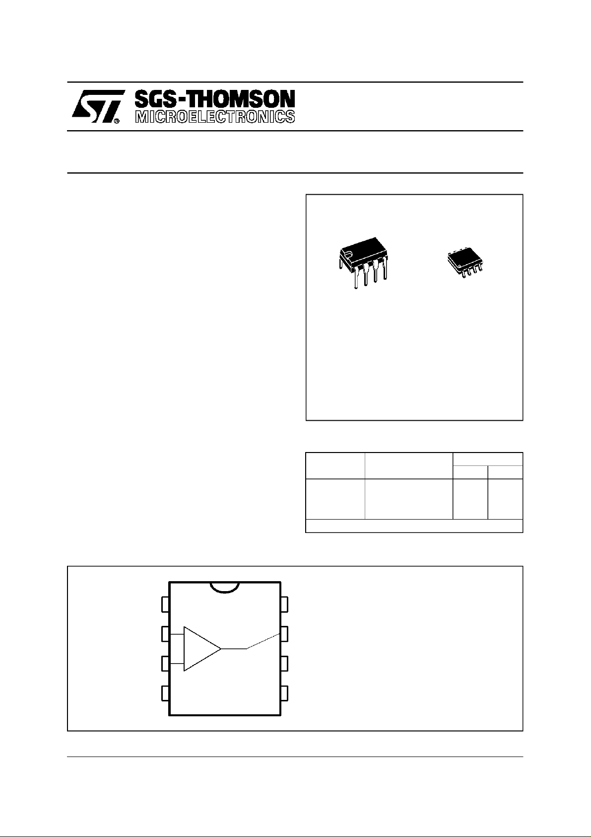
PIN CONNECTIONS (top view)
1
2
3
+
-
N
DIP8
(Plastic Package)
ORDER CODES
CC
CC
-
+
Temperature
Part Number
LM111 –55, 125
LM211 –40, 105
LM311 0, 70
Example : LM311D
8
7
6
1 - Ground
2 - Non-inverting input
3 - Inverting input
4-V
5 - Balance
6 - Strobe/balance
7 - Output
8-V
D
SO8
(Plastic Micropackage)
Package
Range
o
C ••
o
C ••
o
C ••
ND
October1997
4
5
1/9
LM111 - LM2 11 - LM311
SCHEMATIC DIAGRAM
Strobe/balance
Non-inverting
input
Inverting
input
300
Q5
Q1
R3
Ω
R1
1.3k
D1
5V
Balance
R4
Ω
300
R8
Q9
Q22
Ω
Q10
600
R17
60
R15
450
R14
2k
R9
Ω
Q20
Q11
Q19
R16
400
Q18
Ω
R10
4k
Ω
Q14
Ω
Ω
Q17
Ω
Q16
Q6
R2
Ω
1.3k
Ω
1.2k
Q3
D2
5V
Q2
250
R6
R19
Ω
Ω
Q4
Q23
R5
70
R7
1.2k
Ω
Q7
Ω
R18
200
750
Q8
Q21
Ω
Q13
Collector o u tput
V
CC
Q12
R11
Ω
130
R12
Ω
600
V
CC
Q15
R13
4
Ω
Emitter output or ground
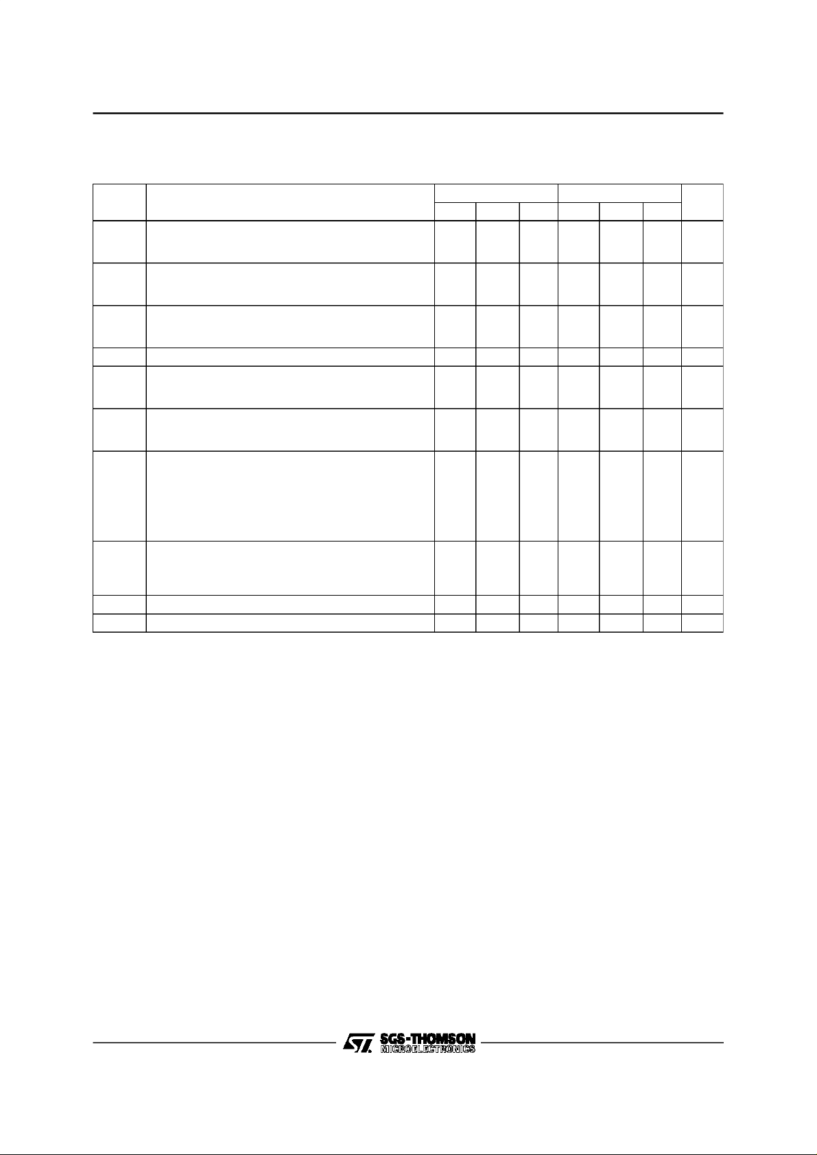
ABSOLUTE MAXIMUM RATINGS
Symbol Parameter LM111 LM211 LM311 Unit
V
CC
V
id
V
i
P
tot
T
oper
T
stg
V
(1–4)
V
(7–4)
Outputshort-circuitduration : 10s LM111: +150oC
Voltage atstrobe pin : V
Note : 1. This rating applies for ±15V supplies. The positive input voltage limit is30V above the negative. Thenegativeinput voltagelimit is
2/9
Supply Voltage 36 36 36 V
Differential Input Voltage ±30 ±30 ±30 V
Input Voltage – (note 1) ±15 ±15 ±15 V
Power Dissipation 500 mW
Operating Free-air Temperature Range –55 to +125 –40 to +105 0 to +70
Storage Temperature Range –65 to +150 –65 to +150 –65 to +150
Ground to Negative Supply Voltage 30 30 30 V
Output to Negative Supply Voltage 50 50 40 V
+
–5V Maximum junction temperature LM211 : +150oC
CC
equal to the negative supply voltageor 30V below thepositive supply, whichever is less.
LM311: +150
o
C
o
C
o
C
LM111 - LM211 - LM311
ELECTRICAL CHARACTERISTICS
= ±15V, T
V
CC
Symbol Parameter
Input Offset Voltage (RS≤ 50kΩ) – (note 1)
V
io
Input Offset Current – (note 1)
I
io
Input Bias Current – (note 1)
I
ib
Large Signal Voltage Gain 40 200 40 200 V/mV
A
vd
Supply Currents
+
I
CC
-
I
CC
Input Common Mode Voltage Range
V
icm
V
Low Level Output Voltage
OL
High Level Output Current
I
OH
I
Notes: 1. The offset voltage,offset current and bias current specificationsapply for any supply voltage froma single+5V supply up to ±15V
Strobe Current 3 3 mA
strobe
Response Time – (note 2) 200 200 ns
t
re
supplies.
The offset voltages and offset currents given are the maximumvalues requiredto drive the outputdown to +1V or upto +14V with
a 1mA load current. Thus,these parameters define an errorband and take into accountthe worst-case of voltagegain and input
impedance.
2. The response time specified(see definitions) is for a 100mV input step with5mV overdrive.
=25oC(unless otherwise specified)
amb
= +25oC
T
amb
. ≤ T
T
min
T
amb
. ≤ T
T
min
T
amb
. ≤ T
T
min
amb
= +25oC
amb
= +25oC
amb
≤ T
≤ T
≤ T
max
max
max
.
.
.
Positive
Negative
. ≤ T
T
min
T
amb
T
min.
+
≥ +4.5 V, V
V
CC
= 8mA V
I
o
T
amb
. ≤ T
T
min
≤ T
amb
= +25oC, IO= 50mA V
≤ T
amb
= +25oCV
amb
. -14.5 +13.8
max
-5mV
i ≤
-10mV
V
≤ T
.
max
-
CC
≤ T
.V
max
=0
i ≤
-6mV
i ≤
-10mV
V
i ≤
≥+ 5mV, VO= +35V
i
≥ +10mV, VO=+5V
V
i
≥+ 5mV, VO= +35V
i
LM111 - LM211 LM311
Min. Typ. Max. Min. Typ. Max.
0.7 3
4
410
20
60 100
150
5.1
4.1
6
5
+13
-14.7
0.75
0.23
1.5
0.4
-14.5
2 7.5
10
650
70
100 250
300
5.1
7.5
4.1
+13.8
5
+13
-14.7
0.75
0.23
1.5
0.4
0.2
0.2 50nAnA
0.1100.5
Unit
mV
nA
nA
mA
µA
V
V
3/9
 Loading...