

LM19 3 - LM293
LOWPOWER DUAL VOLTAGE COMPARATORS
.WIDESINGLESUPPLYVOLTAGERANGEOR
DUAL SUPPLIES +2V TO +36V OR ±1V TO
±18V
.VERY LOW SUPPLY CURRENT (0.4mA)
INDEPENDENTOF SUPPLYVOLTAGE
(1 mW/comparatorat +5V)
.LOW INPUT BIASCURRENT : 25nATYP
.LOW INPUT OFFSET CURRENT : ±5nATYP
.LOW INPUT OFFSET VOLTAGE: ±1mV TYP
.INPUT COMMON-MODE VOLTAGE RANGE
INCLUDES GROUND
.LOW OUTPUT SATURATION VOLTAGE :
250mV TYP.(I
=4mA)
O
.DIFFERENTIAL INPUT VOLTAGE RANGE
EQUALTOTHESUPPLYVOLTAGE
.TTL, DTL, ECL, MOS, CMOS COMPATIBLE
OUTPUTS
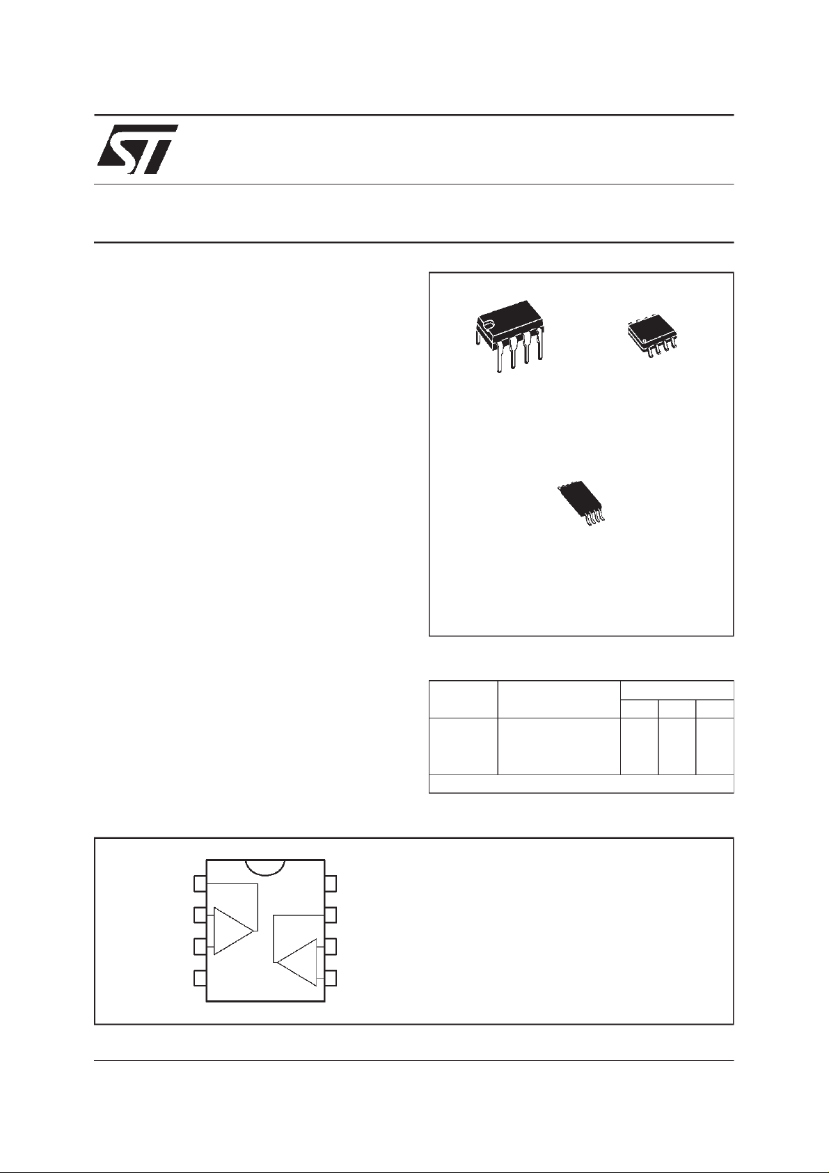
N
DIP8
(PlasticPackage)
(Thin Shrink Small Outline Package)
(PlasticMicropackage)
P
TSSOP8
LM393
D
SO8
DESC RIP TI ON
These devices consist of two independent low
powervoltagecomparatorsdesignedspecificallyto
operatefrom a single supply overa wide range of
voltages.Operationfromsplitpowersuppliesisalso
possible.
Thesecomparatorsalsohaveauniquecharacteristic in that the input common-modevoltagerange
includesgroundeventhoughoperatedfroma single
powersupplyvoltage.
PI N CONNECTIONS (top view)
1
2
-
+
3
45
8
7
6
-
+
ORDER CODES
Part
Number
LM193 –55, +125
LM293 –40, +105
LM393 0, +70
Example : LM393D
1 - Output1
2 - Invertinginput 1
3 - Non-inverting input 1
4-V
5 - Non-inverting input 2
6 - Invertinginput 2
7 - Output2
8-V
CC
CC
-
+
Temperature
Range
Package
o
C •••
o
C •••
o
C •••
NDP
June 1998
1/10
LM193 - LM293 - LM 393
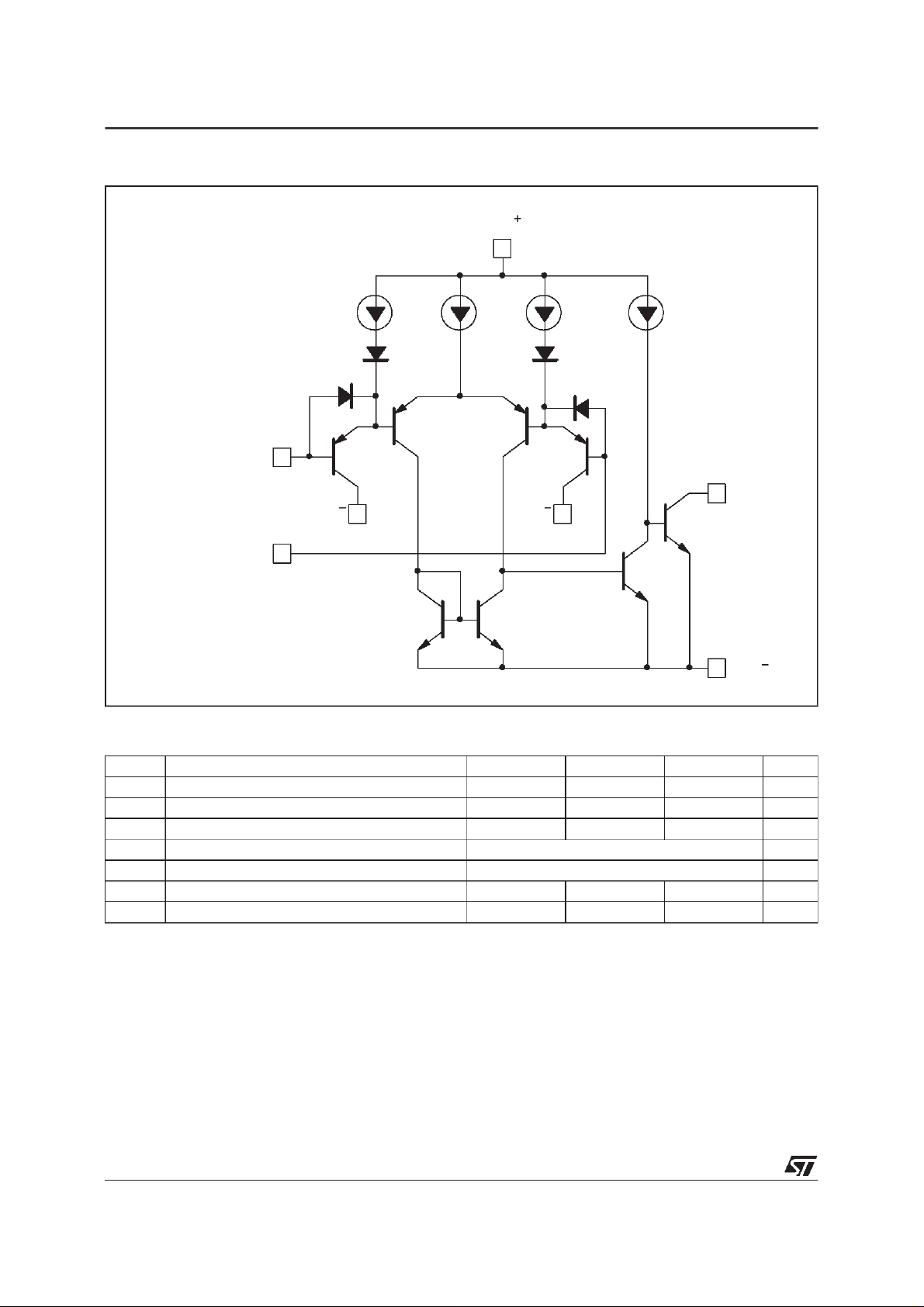
SCHE MATIC DIAGRAM (1/2 LM193)
V
CC
3.5µA100
µ
A 3.5µA 100µA
Non-inverting
Input
V
V
CC
V
CC
O
Inverting
Input
V
CC
ABSOLUTE MAXIMUM RATINGS
Symbol Parameter LM193 LM293 LM393 Unit
V
P
T
T
Notes : 1. Sho r t-cir cuit f r om t he output to V
Supply Voltage ±18 or 36 ±18 or 36 ±18 or 36 V
CC
Differential Input Voltage ±36 ±36 ±36 V
V
id
Input Voltage –0.3 to +36 –0.3 to +36 –0.3 to +36 V
V
i
Output Short-circuit to Ground – (note 1) Infinite
Power Dissipation 830 mW
tot
Operating Free-air TemperatureRange –55 to +125 –40 to +105 0 to +70
oper
Storage Temperature Range –65 to +150 –65 to +150 –65 to +150
stg
+
can cause excessive heati ng and eventual destruction. T he maxi mum out pu t
curr ent is approximately 20mA, independent of the magnitude of V
CC
+
.
CC
o
C
o
C
2/10
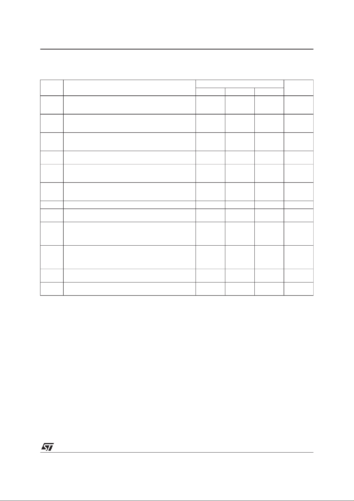
ELECTRICAL CHARACTERISTICS
V
CC
+
= +5V, V
CC
–
= 0V, T
=25oC (unless otherwise specified)
amb
Symbol Parameter
Input Offset Voltage – (note 2)
V
io
Input Bias Current – (note 3)
I
ib
Input Offset Current
I
io
A
V
I
V
I
Notes : 2. At output switch p oint, VO≈ 1.4V, RS=0Ωwit h V
Large Signal Voltage Gain
vd
I
Supply Current (all comparators)
CC
Input Common Mode Voltage Range - (note 4)
icm
Differential Input Voltage - (note 6) V
V
id
Output Sink Current
sink
Low Level Output Voltage
OL
High Level Output Current
OH
Response Time
t
re
t
Large Signal Response Time
rel
(0V to V
3. T he dir ection of t he input curre nt is o ut of the IC d ue to the PN P input stage . Thi s curr ent i s essentially const ant ,
independent of the stat e of the out put, so no loading charge exists on the re ference or input l i nes.
4. T he input common-mode vo ltage of eit her inp ut signal vol t age should not be allow ed to go negative by more than
0.3V .
The upper end of the common- mode voltage r ange is V
damage.
5. T he r esponse ti m e specified is for a 100m V input step w ith 5mV overdri ve. For lar ger overdr i ve signals 300ns
can be obtai ne d.
6. P ositive excursions of i nput volt age may ex ceed the pow er supply level. As l ong as the other vol t age remains
wit hin the comm on- mode range t he com parator willprovi de a pr oper outpu t state. The low input volt age state must
not be less than –0.3V (or 0.3V below the negat i ve power supply, if used).
= +25oC
T
amb
. ≤ T
T
min
T
amb
. ≤ T
T
min
T
amb
. ≤ T
T
min
= 15V, RL= 15kΩ,Vo= 1 to 11V 50 200
V
CC
= 5V, no load
V
CC
= 30V, no load
V
CC
T
amb
. ≤ T
T
min
= -1V, VO= 1.5V) 6 16
(V
id
= -1V, I
(V
id
T
amb
. ≤ T
T
min
= 1V, VCC=VO= 30V)
(V
id
T
amb
. ≤ T
T
min
= 5.1kΩ to V
(R
L
=TTL,V
(V
i
amb
= +25oC
amb
= +25oC
amb
= +25oC
amb
=25oC
amb
=25oC
amb
+
1.5V) .
CC
≤ T
max.
≤ T
max.
≤ T
max.
≤ T
max.
= 4mA)
sink
≤ T
max
≤ T
max
+
) – (note 5) 1.3
CC
= +1.4 V, RL= 5.1kΩ to V
ref
CC
LM193 - LM293 - LM393
LM193 - LM293 - LM393
Min. Typ. Max.
15
25 250
550
0.4
1
0
0
250 400
0.1
+
) 300
+
fr om 5V to 30V and over the fu l l input commo n- mode range
CC
+
–1.5V , but e ither or both inputs can go to +30V without
CC
9
400
150
1
2.5
+
V
-1.5
CC
+
-2
V
CC
+
CC
700
1
Unit
mV
nA
nA
V/mV
mA
V
V
mA
mV
nA
µA
µs
ns
3/10
 Loading...