

Datasheet LM319N, LM319D, LM219N, LM219D, LM219 Datasheet (SGS Thomson Microelectronics)
...
HIGH SPEED DUAL COMPARATORS
.TWO INDEPENDENTCOMPARATORS
.OPERATESFROMA SINGLE +5VSUPPLY
.TYPICALLY80nsRESPONSETIMEAT ±15V
.MINIMUMFAN-OUT OF 2 EACHSIDE
.MAXIMUM INPUT CURRENT OF 1µA OVER
OPERATINGTEMPERATURERANGE
.INPUTS AND OUTPUTS CAN BE ISOLATED
FROM SYSTEMGROUND
.HIGHCOMMON-MODE SLEWRATE
DESC RIP TI ON
These products are precision high speed dual
comparatorsdesignedto operateoverawiderange
of supplyvoltagesdown to a single5V logicsupply
and ground and have low input currents and high
gains.
The open collector of the output stage makes
compatible with TTL as well as capableof driving
lamps andrelays at currents upto 25mA.
Although designed primarily for applications
requiring operation from digital logic supplies, are
fully specifiedfor power suppliesup to ±15V.
Theyfeaturefasterresponsethanthe LM111atthe
expenseof higherpower dissipation. However,the
high speed, wide operatingvoltage rangeand low
packagecountmake the much more versatile.
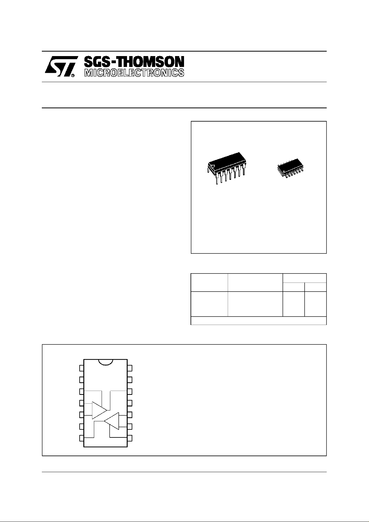
LM119 - LM219
LM319
N
DIP14
(PlasticPackage)
ORDER CODES
Part
Numbe r
LM119 –55, +125oC ••
LM219 –40, +105
LM319 0, +70
Example : LM219N
Temperature
Range
(PlasticMicropackage)
o
C ••
o
C ••
D
SO14
Package
ND
PIN CONNECTIONS (top view)
1
2
3
4
5
6
7
October 1997
+
-
-
+
14
13
12
11
10
9
8
1 - N.C.
2 - N.C.
3 - Ground 1
4 - Non-inverting input 1
5 - Inverting input 1
-
6-V
CC
7 - Output 2
8 - Ground 2
9 - Non-inverting input 2
10 - Inverting input 2
11 - V
12 - Output 1
13 - N.C.
14 - N.C.
CC
+
1/9
LM119 - LM219 - LM319
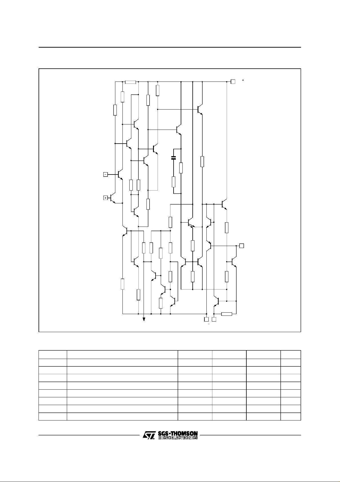
SCHE MATIC DIAGRAM
R2
4k
Ω
R3
4kΩ
3.5k
R1
Ω
R7
3kΩ
R6
3k Ω
Q9
Q4
Q8
V
CC
Inverting
Input
Non-inverting
Input
Q3
Q2
R4
3kΩ
Q1
Q6
Q22
R23
4k
Ω
Q21
R25
600
Ω
R24
250
Ω
Q7
C1
Q6
R5
Ω
3k
Q20
µF
18
R10
470k
R8
Ω
2k
R9
18k
Ω
R22
Ω
60
R20
3.6k
R19
Ω
250
Q19
Q18R21
Ω
900
R11
13k Ω
Ω
R18
Ω
1.8k
Ω
Q11
Q10
R13
600 Ω
R14
2k
R12
13k Ω
Q15
Q13
Q14
Q12
Ω
Q17
R15
300
Ω
Output
Q16
R16
Ω
600
R17
3
Ω
To other half
V
GND
CC
ABSOL UTE MAXIMUM RATINGS
Symbol Parameter LM119 LM219 LM319 Unit
VO-V
2/9
-
CC
-
V
CC
+
V
CC
V
id
V
i
P
tot
T
oper
T
stg
Output to Negative Supply Voltage 36 36 36 V
Negative Supply Voltage 25 25 25 V
Positive Supply Voltage 18 18 18 V
Differential Input Voltage ±5 ±5 ±5V
Input Voltage – (note 1) ±15 ±15 ±15 V
Power Dissipation 500 500 500 mW
Operating Free-air Temperature Range –55 to +125 –40 to +105 0 to +70
Storage Temperature Range –65 to +150 –65 to +150 –65 to +150
o
C
o
C
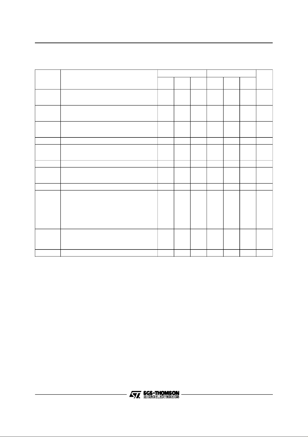
ELEC TRICAL CHARACTERI S TICS
V
CC
= ±15V, T
=25oC(unless otherwisespecified)
amb
Symbol Parameter
LM119 - LM219 - LM319
LM119 - L M219 LM319
Min. Typ. Max. Min. Typ.
Max.
Unit
V
I
io
I
ib
A
I
CC
I
CC
V
icm
V
V
OL
I
OH
t
re
Notes : 1. For s upply voltages less than ±15V t he absolut e maxim um input vol tage i s equal t o the supply voltage.
Input Offset Voltage (RS≤ 5kΩ) – (note 2)
io
T
T
amb
min
= +25oC
. ≤ T
amb
≤ T
max.
0.7 4
7
28
Input Offset Current – (note 2)
T
T
amb
min
= +25oC
. ≤ T
amb
≤ T
max.
30 75
100
80 200
Input Bias Current – (note 2)
= +25oC
T
amb
. ≤ T
T
min
Large Signal Voltage Gain 10 40 8 40 V/mV
vd
+
Positive Supply Current
–
Negative Supply Current 3 4.5 3 5 mA
V
V
CC
CC
= ±15V
+
amb
= +5V, V
≤ T
CC
max.
–
=0V
150 500
1000
8
11.5 8
4.3
250 1000
1200
4.3
Input Common Mode Voltage Range
= ±15V
V
CC
+
= +5V, V
V
CC
Differential Input Voltage ±5 ±5V
id
CC
–
=0V
±121±13
±121±13
3
Low Level Output Voltage
= +25oC, IO= 25mA
T
amb
T
min.
V
CC
≤ T
amb
+
≥ +4.5V, V
≤ T
max.
CC
–
= 0V, I
≤ –5mV
V
i
≤ –10mV
V
i
O(sink)
≤ –6mV
V
i
≤ –10mV
V
i
< 3.2mA
0.75
0.23
1.5
0.75
0.4
0.3
High Level Output Current (VO= +35V)
= +25oCV
T
amb
. ≤ T
T
min
amb
≤ T
max
≥5mV
i
≥ 10mV
V
i
.Vi≥5mV
0.2
1
2
0.2 10
10
Response Time – (note 3) 80 80 ns
2. These sp eci fi c at ions apply for V
bi as c ur r ent specificat ions a ppl y for any supply v oltage f r om a single +5V suppl y up to ±15V supplies.
T he offset vol t ages and o f f set c u r r ent given a r e the m aximum values r equir ed to drive t he output down t o 1V
or up to +14V w it h a 1mA l oad c ur r ent.
T hus, t hese parameter s defi ne an err or band and take in t o acc ount the worst case effects of vol t age gain
and i nput impedance.
3. The r esponse time speci f ied is for a 1 00mV input st ep w ith 5mV ov er driv e.
= ±15V, unless other w ise stated. T he of fset volt age, off set c urrent and
CC
10
300
12.5
3
1.5
0.4
mV
nA
nA
mA
V
V
µA
3/9

LM119 - LM219 - LM319
4/9

LM119 - LM219 - LM319
5/9

LM119 - LM219 - LM319
6/9
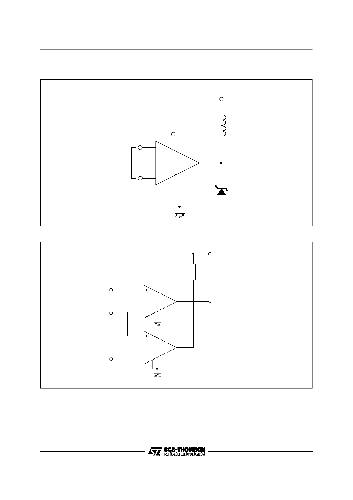
TYP ICAL APPLIC ATI ON DIAGRAMS
RELAY DRIVER
Inputs
LM119 - LM219 - LM319
+28V
+5V
1/2
LM119
30V
WINDOW DETECTOR
+5V
500Ω
V
UT
1/2
LM119
V
I
1/2
LM119
V
LT
V
O
V
O
= +5V for
= 0 for
V
O
TTL output
V
V
LT
V
V
<>
I
V
<<
I
V
or
LT
UT
V
I
UT
7/9

LM119 - LM219 - LM319
PACKAG E MECHANICAL DATA
14 PINS – PLASTIC DIP
Dime nsi o ns
Millime ters Inches
Min. Typ. Max. Min. Typ. Max.
a1 0.51 0.020
B 1.39 1.65 0.055 0.065
b 0.5 0.020
b1 0.25 0.010
D 20 0.787
E 8.5 0.335
e 2.54 0.100
e3 15.24 0.600
F 7.1 0.280
i 5.1 0.201
L 3.3 0.130
Z 1.27 2.54 0.050 0.100
PM-DIP14.EPS
DIP14.TBL
8/9

PACKAG E MECHANICAL DATA
14 PINS – PLAS TI C MI CROPA CKA G E (SO )
LM119 - LM219 - LM319
Dime nsi o ns
Millime ters Inches
Min. Typ. Max. Min. Typ. Max.
A 1.75 0.069
a1 0.1 0.2 0.004 0.008
a2 1.6 0.063
b 0.35 0.46 0.014 0.018
b1 0.19 0.25 0.007 0.010
C 0.5 0.020
c1 45
D 8.55 8.75 0.336 0.334
E 5.8 6.2 0.228 0.244
e 1.27 0.050
e3 7.62 0.300
F 3.8 4.0 0.150 0.157
G 4.6 5.3 0.181 0.208
L 0.5 1.27 0.020 0.050
M 0.68 0.027
S8
Information furnished is believed to be accurate and reliable. However, SGS-THOMSON Microelectronics assumes no responsibility for the consequences of use of such information nor for any infringement of patents or other rights of third parties which
may result from its use. No license is granted by implication or otherwise under any patent or patent rights of SGS-THOMSON
Microelectronics. Specification mentioned in this publication are subject to change without notice. This publication supersedes
and replaces all information previously supplied. SGS-THOMSON Microelectronics products are not authorized for use as critical
components in life support devices or systems without express written approval of SGS-THOMSON Microelectronics.
o
(typ.)
o
(max.)
PM-SO14.EPS
SO14.TBL
1997 SGS-THOMSON Microelectronics – Printed in Italy – All Rights Reserved
SGS-THOMSON Microelectronics GROUP OF COMPANIES
Australia - Brazil - Canada - China - France - Germany - Hong Kong - Italy - Japan - Korea - Malaysia - Malta - Morocco
The Netherlands - Singapore - Spain - Sweden - Switzerland - Taiwan - Thailand - United Kingdom - U.S.A.
ORDERCODE :
9/9
 Loading...