

SGS Thomson Microelectronics LIS3L02AS Datasheet
3Axis - 2g/6g LINEAR ACCELEROMETER
■ 3V TO 5.25V SINGLE SUPPLY OPERATION
■ THE SENSITIVITY IS ADJUSTED WITH A
TOTAL ACCURACY OF ±10%
■ THE OUTPUT VOLTAGE, OFFSET,
SENSITIVITY AND TEST VOLTAGE ARE
RATIOMETRIC TO THE SUPPLY VOLTAGE
■ DEVICE SENSITI VITY IS ON-CHI P FACTORY
TRIMMED
■ EMBEDDED SELF TEST
■ HIGH SHOCK SURVIVABILITY
DESCRIPTION
The LIS3L02AS is a t ri-axis linear accelerometer
that includes a sensing element and an IC interface able to take the information from the sensing
element and to provide an analog signal to the external world.
The sensing element, capable to detect the acceleration, is manufactured using a dedicated process called THELMA (Thick Epi-Poly Layer for
Microactuators and Accelerometers) developed
by ST to produce inertial sensors and actuators in
silicon.
The IC interface instead is manufactured us ing a
CMOS process that allows high level of integration
to design a dedicated circuit which is trimmed to
better match the sensing element characteristics.
The LIS3L02AS has a user selectable full scale of
LIS3L02AS
INERTIAL SENSOR:
PRODUCT PREVIEW
SO-24
ORDERING NUMB ER: LIS3L 02AS
2g, 6g and it is capable of measuring accelerations
over a maximum bandwidth of 4.0 K Hz for the X
and Y axis and 2.5KHz for the Z axis. The device
bandwidth may be reduced by using external capacitances. A self-test capability allows the user to
check the functi o n ing of th e syst e m.
The LIS3L02AS is a vailable in plastic SM D package and it is specified over a temperature range
extending from -40°C to +85°C.
The LIS3L02AS belongs to a family of products
suitable for a variety of applications:
– Antitheft systems
– Inertial navigation
– Virtual reality input devices
– Vibration Monitoring, recording and com pen-
sation
– Appliance control
– Robotics
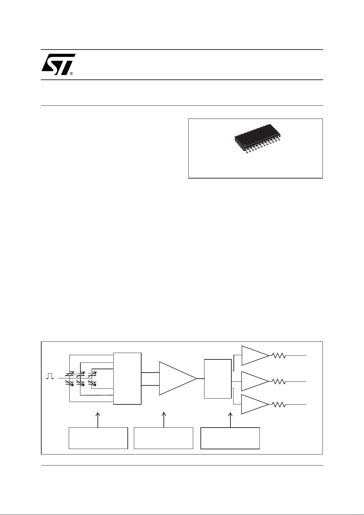
BLOCK DIAGRAM
S1X
S1Y
S1Z
rot
S2Z
S2Y
S2X
VOLTAGE & CURRENT
REFERENCE
February 2003
This is preliminary information on a new product now in development. Details are subject to change without notice.
MUX
TRIMMING CIRCUIT
TEST INTERFACE
AMPLIFIE R
DEMUX
CLOCK
&
PHASE GENERATOR
S/HCHARGE
S/H
S/H
&
Routx
Routy
Routz
Voutx
Vouty
Voutz
1/7

LIS3L02AS
PIN DESCRIPTION
N° Pin Function
1 to 6 NC Internally not connected
7 Reserved Leave unconnected or connect to ground
8 Reserved Leave unconnected or connect to Vdd
9 Reserved Connect to Vdd or ground
10-11 Reserved Leave unconnected or connect to Vdd
12 FS Full Scale selection (Logic 0: 2g Full-scale; Logic 1: 6g Full-scale)
13 Voutz Output Voltage
14 PD Power Down (Logic 0: normal mode; Logic 1: Power-Down mode)
15 Voutx Output Voltage
16 ST Self Test (Logic 0: normal mode; Logic 1: Self-test)
17 Vouty Output Voltage
18 Vdd Power supply
19 GND 0V supply
20 to 24 NC Internally not connected
PIN CONNECTION (Top view )
X
Z
13
Y
1
Reserved
DIRECTION OF THE
DETECTABLE
ACCELERATIONS
Reserved
Reserved
Reserved
Reserved
NC
NC
NC
NC
NC
NC
FS
NC
NC
NC
NC
NC
GND
Vdd
Vouty
ST
Voutx
PD
Voutz
2/7

LIS3L02AS
ELECTRICAL CHARACTERISTCS (Temperature range -40°C to +85°C)
Symbol Parameter Test Condition Min. Typ. Max. Unit
Vdd Supply voltage 3 5.25 V
Idd Supply current 1.0 mA
Voff Zero-g level T = 25°C
ratiometric to Vdd
Ar Acceleration range 0V on FS pin ±1.8 ±2.0 ±2.2 g
Vdd on FS pin ±±6.0 g
So Sensitivity ratiometric to Vdd T = 25°C
NL Non Linearity Best fit straight line
fuc Sensing Element Resonant
Frequency
an Accel eration noise density Vdd=5V
Vt Self test output voltage
Ratiometric to Vdd
Vst Self test input Logic 0 level 0 0.8 V
Full-scale = 2g
T = 25°C
Full-scale = 6g
X, Y axis
Full-scale = 2g
Best fit straight line
Z axis
Full-scale = 2g
X, Y axis 4.0 KHz
Z axis 2.5 KHz
Full-scale = 2g
T = 25°C
@ 5V
Vdd/2-10% Vdd/2 Vdd/2+10% V
Vdd/5–10% Vdd/5 Vdd/5+10% V/g
Vdd/15–10% Vdd/15 Vdd/15+10% V/g
±0.3 %
±0.6 %
100
TBD V
µg/
Hz
Logic 1 level 2.8 Vdd V
Rout Output impedance 100
Cload Capacitive load drive 320 pF
kΩ
1 FUNCTIONALITY
1.1 Sensing element
The THELMA proces s is utilized to c reate a surfac e micro-mach ined accelerom eter. The technolo gy allows to carry out suspended silicon structures which are attached to the substrate in a few points called
anchors and free to move on a plane parallel to the subst rate itself. To b e com pati ble with the tradi tional
packaging techniques a cap is placed on top of t he sensing element to avoi d blockin g the moving p arts
during the molding phase.
The equivalent circuit for the sensing element is shown in t he below figure; when a linear acceleration is
applied, the proof mass di splaces from its nominal po sition, c ausing an imbalance in t he cap acitive hal fbridge. This imbalance is measured using charge integration in response to a voltage pulse applied to the
sense capacitor.
The nominal value of the capacitors, at steady state, is few pF and when an acceleration is applied the
maximum variation of the capacitive load is few tenth of pF.
3/7
 Loading...