

2-axis - ±2g/±8g smart digital output “piccolo” accelerometer
Feature
■ 2.16V to 3.6V supply voltage
■ 1.8V compatible IOs
■ <1mW power consumption
■ ±2g/±8g dynamically selectable Full-Scale
2
■ I
C/SPI digital output interface
■ Programmable interrupt generator
■ Click and double click recognition
■ Embedded high pass filter
■ Embedded self test
■ 10000g high shock survivability
■ ECOPACK® RoHS and “Green” compliant
(see Section 9)
LIS202DL
MEMS motion sensor
LGA-14
measuring accelerations with an output data rate
of 100Hz or 400Hz.
A self-test capability allows the user to check the
functioning of the sensor in the final application.
(3x5x0.9mm)
Description
The LIS202DL is an ultra compact low-power two
axes linear accelerometer. It includes a sensing
element and an IC interface able to provide the
measured acceleration to the external world
through I
The sensing element, capable of detecting the
acceleration, is manufactured using a dedicated
process developed by ST to produce inertial
sensors and actuators in silicon.
The IC interface is manufactured using a CMOS
process that allows to design a dedicated circuit
which is trimmed to better match the sensing
element characteristics.
The LIS202DL has dynamically user selectable
full scales of ±2g/±8g and it is capable of
Table 1. Device summary
2
C/SPI serial interface.
Part number Temp range, ° CPackage Packing
LIS202DL -40 to +85 LGA Tray
LIS202DLTR -40 to +85 LGA Tape and reel
The device may be configured to generate inertial
wake-up interrupt signals when a programmable
acceleration threshold is crossed at least in one of
the two axes. Thresholds and timing of interrupt
generators are programmable by the end user on
the fly.
The LIS202DL is available in plastic Thin Land
Grid Array package (TLGA) and it is guaranteed
to operate over an extended temperature range
from -40°C to +85°C.
The LIS202DL belongs to a family of products
suitable for a variety of applications:
– Motion activated functions
– Gaming and Virtual Reality input
devices
– Vibration Monitoring and Compensation
June 2007 Rev 1 1/36
www.st.com
36

Contents LIS202DL
Contents
1 Block diagram & pin description . . . . . . . . . . . . . . . . . . . . . . . . . . . . . . . 4
1.1 Block diagram . . . . . . . . . . . . . . . . . . . . . . . . . . . . . . . . . . . . . . . . . . . . . . . 4
1.2 Pin description . . . . . . . . . . . . . . . . . . . . . . . . . . . . . . . . . . . . . . . . . . . . . . 4
2 Mechanical and electrical specifications . . . . . . . . . . . . . . . . . . . . . . . . 6
2.1 Mechanical characteristics . . . . . . . . . . . . . . . . . . . . . . . . . . . . . . . . . . . . . 6
2.2 Electrical characteristics . . . . . . . . . . . . . . . . . . . . . . . . . . . . . . . . . . . . . . . 7
2.3 Absolute maximum ratings . . . . . . . . . . . . . . . . . . . . . . . . . . . . . . . . . . . . . 8
2.4 Terminology . . . . . . . . . . . . . . . . . . . . . . . . . . . . . . . . . . . . . . . . . . . . . . . . 9
2.4.1 Sensitivity . . . . . . . . . . . . . . . . . . . . . . . . . . . . . . . . . . . . . . . . . . . . . . . . . 9
2.4.2 Zero-g level . . . . . . . . . . . . . . . . . . . . . . . . . . . . . . . . . . . . . . . . . . . . . . . 9
2.4.3 Self test . . . . . . . . . . . . . . . . . . . . . . . . . . . . . . . . . . . . . . . . . . . . . . . . . . 9
2.4.4 Click and double click recognition . . . . . . . . . . . . . . . . . . . . . . . . . . . . . . 9
3 Functionality . . . . . . . . . . . . . . . . . . . . . . . . . . . . . . . . . . . . . . . . . . . . . . 10
3.1 Sensing element . . . . . . . . . . . . . . . . . . . . . . . . . . . . . . . . . . . . . . . . . . . . 10
3.2 IC interface . . . . . . . . . . . . . . . . . . . . . . . . . . . . . . . . . . . . . . . . . . . . . . . . 10
3.3 Factory calibration . . . . . . . . . . . . . . . . . . . . . . . . . . . . . . . . . . . . . . . . . . 10
4 Application hints . . . . . . . . . . . . . . . . . . . . . . . . . . . . . . . . . . . . . . . . . . . 11
4.1 Soldering information . . . . . . . . . . . . . . . . . . . . . . . . . . . . . . . . . . . . . . . . 11
5 Digital interfaces . . . . . . . . . . . . . . . . . . . . . . . . . . . . . . . . . . . . . . . . . . . 12
5.1 I2C serial interface . . . . . . . . . . . . . . . . . . . . . . . . . . . . . . . . . . . . . . . . . . 12
5.1.1 I2C operation . . . . . . . . . . . . . . . . . . . . . . . . . . . . . . . . . . . . . . . . . . . . . 13
5.2 SPI bus interface . . . . . . . . . . . . . . . . . . . . . . . . . . . . . . . . . . . . . . . . . . . 14
5.2.1 SPI read . . . . . . . . . . . . . . . . . . . . . . . . . . . . . . . . . . . . . . . . . . . . . . . . . 16
5.2.2 SPI write . . . . . . . . . . . . . . . . . . . . . . . . . . . . . . . . . . . . . . . . . . . . . . . . 16
5.2.3 SPI read in 3-wires mode . . . . . . . . . . . . . . . . . . . . . . . . . . . . . . . . . . . 17
6 Register mapping . . . . . . . . . . . . . . . . . . . . . . . . . . . . . . . . . . . . . . . . . . 18
7 Register description . . . . . . . . . . . . . . . . . . . . . . . . . . . . . . . . . . . . . . . . 20
2/36

LIS202DL Contents
7.1 WHO_AM_I (0Fh) . . . . . . . . . . . . . . . . . . . . . . . . . . . . . . . . . . . . . . . . . . . 20
7.2 CTRL_REG1 (20h) . . . . . . . . . . . . . . . . . . . . . . . . . . . . . . . . . . . . . . . . . . 20
7.3 CTRL_REG2 (21h) . . . . . . . . . . . . . . . . . . . . . . . . . . . . . . . . . . . . . . . . . . 21
7.4 CTRL_REG3 [Interrupt CTRL register] (22h) . . . . . . . . . . . . . . . . . . . . . . 22
7.5 HP_FILTER_RESET (23h) . . . . . . . . . . . . . . . . . . . . . . . . . . . . . . . . . . . . 23
7.6 STATUS_REG (27h) . . . . . . . . . . . . . . . . . . . . . . . . . . . . . . . . . . . . . . . . . 23
7.7 OUT_X (29h) . . . . . . . . . . . . . . . . . . . . . . . . . . . . . . . . . . . . . . . . . . . . . . 23
7.8 OUT_Y (2Bh) . . . . . . . . . . . . . . . . . . . . . . . . . . . . . . . . . . . . . . . . . . . . . . 23
7.9 WU_CFG_1 (30h) . . . . . . . . . . . . . . . . . . . . . . . . . . . . . . . . . . . . . . . . . . 24
7.10 WU_SRC_1 (31h) . . . . . . . . . . . . . . . . . . . . . . . . . . . . . . . . . . . . . . . . . . 24
7.11 WU_THS_1 (32h) . . . . . . . . . . . . . . . . . . . . . . . . . . . . . . . . . . . . . . . . . . . 25
7.12 WU_DURATION_1 (33h) . . . . . . . . . . . . . . . . . . . . . . . . . . . . . . . . . . . . . 25
7.13 WU_CFG_2 (34h) . . . . . . . . . . . . . . . . . . . . . . . . . . . . . . . . . . . . . . . . . . 26
7.14 WU_SRC_2 (35h) . . . . . . . . . . . . . . . . . . . . . . . . . . . . . . . . . . . . . . . . . . 26
7.15 WU_THS_2 (36h) . . . . . . . . . . . . . . . . . . . . . . . . . . . . . . . . . . . . . . . . . . . 27
7.16 WU_DURATION_2 (37h) . . . . . . . . . . . . . . . . . . . . . . . . . . . . . . . . . . . . . 27
7.17 CLICK_CFG (38h) . . . . . . . . . . . . . . . . . . . . . . . . . . . . . . . . . . . . . . . . . . 28
7.18 CLICK_SRC (39h) . . . . . . . . . . . . . . . . . . . . . . . . . . . . . . . . . . . . . . . . . . 29
7.19 CLICK_THSY_X (3Bh) . . . . . . . . . . . . . . . . . . . . . . . . . . . . . . . . . . . . . . . 29
7.20 CLICK_TimeLimit (3Dh) . . . . . . . . . . . . . . . . . . . . . . . . . . . . . . . . . . . . . . 29
7.21 CLICK_Latency (3Eh) . . . . . . . . . . . . . . . . . . . . . . . . . . . . . . . . . . . . . . . 30
7.22 CLICK_Window (3Fh) . . . . . . . . . . . . . . . . . . . . . . . . . . . . . . . . . . . . . . . 30
8 Typical performance characteristics . . . . . . . . . . . . . . . . . . . . . . . . . . . 31
8.1 Mechanical characteristics at 25°C . . . . . . . . . . . . . . . . . . . . . . . . . . . . 31
8.2 Mechanical Characteristics derived from measurement in the -40°C to
+85°C temperature range . . . . . . . . . . . . . . . . . . . . . . . . . . . . . . . . . . . . 32
8.3 Electro-mechanical characteristics at 25°C . . . . . . . . . . . . . . . . . . . . . . . 33
9 Package information . . . . . . . . . . . . . . . . . . . . . . . . . . . . . . . . . . . . . . . . 34
10 Revision history . . . . . . . . . . . . . . . . . . . . . . . . . . . . . . . . . . . . . . . . . . . 35
3/36
Block diagram & pin description LIS202DL
1 Block diagram & pin description
1.1 Block diagram
Figure 1. Block diagram
X+
I2C
SPI
CS
SCL/SPC
SDA/SDO/SDI
SDO
Y+
a
MUX
Y-
X-
CHARGE
AMPLIFIER
A/D
CONVERTER
CONTROL LOGIC
REFERENCESELF TEST
1.2 Pin description
Figure 2. Pin connection
Y
6
TOP VIEW
Table 2. Pin description
TRIMMING
CIRCUITS
1
CLOCK
CONTROL LOGIC
&
INTERRUPT GEN.
1
INT 1
INT 2
6
X
13
8
13 8
BOTTOM VIEW
Pin# Name Function
1 Vdd_IO Power supply for I/O pins
2 GND 0V supply
3 Reserved Connect to Vdd
4 GND 0V supply
5 GND 0V supply
6 Vdd Power supply
4/36
LIS202DL Block diagram & pin description
Table 2. Pin description (continued)
Pin# Name Function
7CS
SPI enable
2
C/SPI mode selection (1: I2C mode; 0: SPI enabled)
I
8 INT 1 Inertial interrupt 1
9 INT 2 Inertial interrupt 2
10 GND 0V supply
11 Reserved Connect to Gnd
12 SDO
SDA
13
SDI
SDO
14
SCL
SPC
SPI Serial Data Output
2
C less significant bit of the device address
I
2
I
C Serial Data (SDA)
SPI Serial Data Input (SDI)
3-wire Interface Serial Data Output (SDO)
2
I
C Serial Clock (SCL)
SPI Serial Port Clock (SPC)
5/36
Mechanical and electrical specifications LIS202DL
2 Mechanical and electrical specifications
2.1 Mechanical characteristics
(All the parameters are specified @ Vdd=2.5V, T = 25°C unless otherwise noted)
Table 3. Mechanical characteristics
Symbol Parameter Test conditions Min. Typ.
FS Measurement range
(3)
(1)
FS bit set to 0 ±2.0 ±2.3
(2)
Max. Unit
FS bit set to 1 ±8.0 ±9.2
FS bit set to 0 16.2 18 19.8
So Sensitivity
FS bit set to 1 64.8 72 79.2
TCSO
Ty Of f
TCOff
Sensitivity change vs
temperature
Typical zero-g level offset
accuracy
(4),(5)
Zero-g level change vs
temperature
FS bit set to 0 ±0.01 %/°C
FS bit set to 0 ±40 mg
FS bit set to 1 ±60 mg
Max delta from 25°C
±0.5 mg/°C
FS bit set to 0
Vst
Self test output
(6),(7),(8)
change
STP bit used
X axis
Vdd=2.16V to 3.6V
FS bit set to 0
STP bit used
Y axis
-32 -3 LSb
332LSb
Vdd=2.16V to 3.6V
BW System bandwidth
(9)
ODR/2 Hz
Top Operating temperature range -40 +85 °C
g
mg/digit
Wh Product weight 30 mgram
1. The product is factory calibrated at 2.5V. The device can be used from 2.16V to 3.6V
2. Typical specifications are not guaranteed
3. Verified by wafer level test and measurement of initial offset and sensitivity
4. Typical zero-g level offset value after MSL3 preconditioning
5. Offset can be eliminated by enabling the built-in high pass filter
6. If STM bit is used values change in sign for all axes
Self Test output changes with the power supply. Self test “output change” is defined as OUTPUT[LSb]
7.
-OUTPUT[LSb]
8. Output data reach 99% of final value after 3/ODR when enabling Self-Test mode due to device filtering
9. ODR is output data rate. Refer to table 3 for specifications
(Self-test bit on ctrl_reg1=0)
. 1LSb=4.6g/256 at 8bit representation, ±2.3g Full-Scale
(Self-test bit on ctrl_reg1=1)
6/36
LIS202DL Mechanical and electrical specifications
2.2 Electrical characteristics
(All the parameters are specified @ Vdd=2.5V, T= 25°C unless otherwise noted)
Table 4. Electrical Characteristics
Symbol Parameter Test conditions Min. Typ.
(1)
(2)
Max. Unit
Vdd Supply voltage 2.16 2.5 3.6 V
Vdd_IO I/O pins Supply voltage
(3)
1.71 Vdd+0.1 V
Idd Supply current T = 25°C, ODR=100Hz 0.3 0.4 mA
IddPdn
VIH
VIL Digital low level input voltage
VOH High level output voltage
VOL Low level output voltage
Current consumption in
power-down mode
Digital high level input
voltage
T = 25°C 1 5 µA
0.8*Vdd
_IO
0.2*Vdd
_IO
0.9*Vdd
_IO
0.1*Vdd
_IO
DR=0 100
ODR Output data rate
DR=1 400
BW System bandwidth
Ton Turn-on time
(5)
(4)
ODR/2 Hz
3/ODR s
V
V
V
V
Hz
Top Operating temperature range -40 +85
1. The product is factory calibrated at 2.5V. The device can be used from 2.16V to 3.6V
2. Typical specification are not guaranteed
3. It is possible to remove Vdd maintaining Vdd_IO without blocking the communication busses, in this condition the
measurement chain is powered off.
4. Filter cut-off frequency
5. Time to obtain valid data after exiting Power-Down mode
°C
7/36
Mechanical and electrical specifications LIS202DL
2.3 Absolute maximum ratings
Stresses above those listed as “absolute maximum ratings” may cause permanent damage
to the device. This is a stress rating only and functional operation of the device under these
conditions is not implied. Exposure to maximum rating conditions for extended periods may
affect device reliability.
Table 5. Absolute maximum ratings
Symbol Ratings Maximum Value Unit
Vdd Supply voltage -0.3 to 6 V
Vdd_IO I/O pins supply voltage -0.3 to 6 V
Input voltage on any control pin
(CS, SCL/SPC, SDA/SDI/SDO)
Acceleration (any axis, powered, Vdd=2.5V)
-0.3 to Vdd_IO +0.3 V
3000g for 0.5 ms
10000g for 0.1 ms
A
Vin
POW
A
T
UNP
T
STG
Acceleration (any axis, unpowered)
Operating temperature range -40 to +85 °C
OP
Storage temperature range -40 to +125 °C
ESD Electrostatic discharge protection
Note: Supply voltage on any pin should never exceed 6.0V
This is a Mechanical Shock sensitive device, improper handling can cause permanent
damages to the part
This is an ESD sensitive device, improper handling can cause permanent damages to the
part
3000g for 0.5 ms
10000g for 0.1 ms
4.0 (HBM) kV
200 (MM) V
1500 (CDM) V
8/36

LIS202DL Mechanical and electrical specifications
2.4 Terminology
2.4.1 Sensitivity
Sensitivity describes the gain of the sensor and can be determined e.g. by applying 1g
acceleration to it. As the sensor can measure DC accelerations this can be done easily by
pointing the axis of interest towards the center of the earth, noting the output value, rotating
the sensor by 180 degrees (pointing to the sky) and noting the output value again. By doing
so, ±1g acceleration is applied to the sensor. Subtracting the larger output value from the
smaller one and dividing the result by 2 leads to the actual sensitivity of the sensor. This
value changes very little over temperature and also time. The Sensitivity Tolerance
describes the range of Sensitivities of a large population of sensors.
2.4.2 Zero-g level
Zero-g level Offset (TyOff) describes the deviation of an actual output signal from the ideal
output signal if no acceleration is present. A sensor in a steady state on a horizontal surface
will measure 0g in X axis and 0g in Y axis. The output is ideally in the middle of the dynamic
range of the sensor (content of OUT registers 00h, data expressed as 2’s complement
number). A deviation from ideal value in this case is called Zero-g offset. Offset is to some
extent a result of stress to MEMS sensor and therefore the offset can slightly change after
mounting the sensor onto a printed circuit board or exposing it to extensive mechanical
stress. Offset changes little over temperature, see “Zero-g level change vs. temperature”.
The Zero-g level tolerance (TyOff) describes the Standard Deviation of the range of Zero-g
levels of a population of sensors.
2.4.3 Self test
Self Test allows to check the sensor functionality without moving it. The Self Test function is
off when the self-test bit of ctrl_reg1 (control register 1) is programmed to ‘0‘. When the selftest bit of ctrl_reg1 is programmed to ‘1‘ an actuation force is applied to the sensor,
simulating a definite input acceleration. In this case the sensor outputs will exhibit a change
in their DC levels which are related to the selected full scale through the device sensitivity.
When Self Test is activated, the device output level is given by the algebric sum of the
signals produced by the acceleration acting on the sensor and by the electrostatic test-force.
If the output signals change within the amplitude specified inside Tab le 3 , then the sensor is
working properly and the parameters of the interface chip are within the defined
specifications.
2.4.4 Click and double click recognition
The click and double click recognition functions help to create man-machine interface with
little software overload. The device can be configured to output an interrupt signal on
dedicated pin when tapped in any direction.
If the sensor is exposed to a single input stimulus it generates an interrupt request on inertial
interrupt pins (INT1 and/or INT2). A more advanced feature allows to generate an interrupt
request when a “double click” stimulus is applied. A programmable time between the two
events allows a flexible adoption to the application requirements. Mouse-button like
application like clicks and double clicks can be implemented.
This function can be fully programmed by the user in terms of expected amplitude and
timing of the stimuli.
9/36

Functionality LIS202DL
3 Functionality
The LIS202DL is an ultracompact, low-power, digital output 2-axis linear accelerometer
packaged in a LGA package. The complete device includes a sensing element and an IC
interface able to take the information from the sensing element and to provide a signal to the
external world through an I
3.1 Sensing element
A proprietary process is used to create a surface micro-machined accelerometer. The
technology allows to carry out suspended silicon structures which are attached to the
substrate in a few points called anchors and are free to move in the direction of the sensed
acceleration. To be compatible with the traditional packaging techniques a cap is placed on
top of the sensing element to avoid blocking the moving parts during the moulding phase of
the plastic encapsulation.
When an acceleration is applied to the sensor the proof mass displaces from its nominal
position, causing an imbalance in the capacitive half-bridge. This imbalance is measured
using charge integration in response to a voltage pulse applied to the capacitor.
At steady state the nominal value of the capacitors are few pF and when an acceleration is
applied the maximum variation of the capacitive load is in pF range.
2
C/SPI serial interface.
3.2 IC interface
The complete measurement chain is composed by a low-noise capacitive amplifier which
converts the capacitive unbalancing of the MEMS sensor into an analog voltage that is
finally available to the user by analog-to-digital converters.
The acceleration data may be accessed through an I
device particularly suitable for direct interfacing with a microcontroller.
The LIS202DL features a Data-Ready signal (RDY) which indicates when a new set of
measured acceleration data is available thus simplifying data synchronization in the digital
system that uses the device.
The LIS202DL may also be configured to generate an inertial Wake-Up interrupt signal
accordingly to a programmed acceleration event along the enabled axes.
3.3 Factory calibration
The IC interface is factory calibrated for sensitivity (So) and Zero-g level (TyOff).
The trimming values are stored inside the device in a non volatile memory. Any time the
device is turned on, the trimming parameters are downloaded into the registers to be used
during the normal operation. This allows to use the device without further calibration.
2
C/SPI interface thus making the
10/36
LIS202DL Application hints
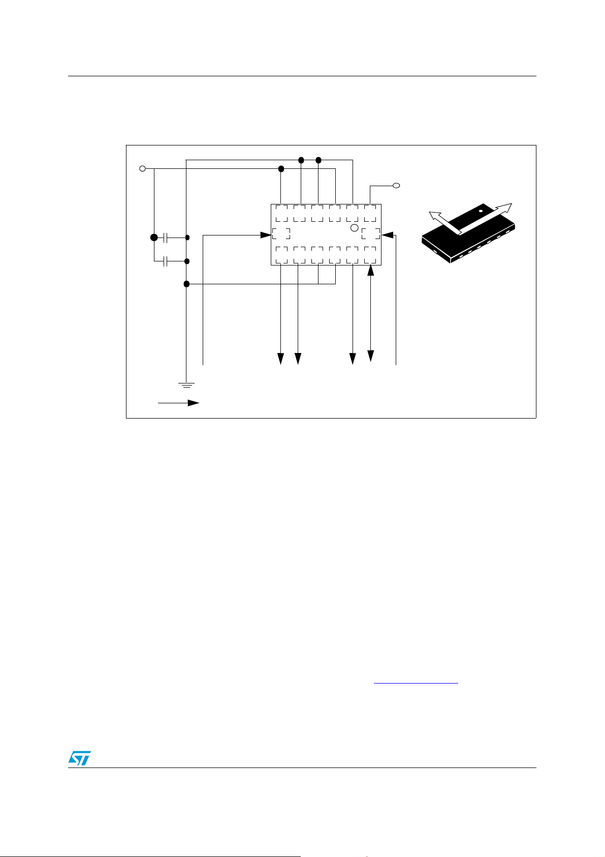
4 Application hints
Figure 3. LIS202DL electrical connection
Vdd
10uF
100nF
GND
6
Top VIEW
8
CS
Digital signal from/to signal controller.Signal’s levels are defined by proper selection of Vdd_IO
INT_2
INT_1
1
SDO
Vdd_IO
13
SDA/SDI/SDO
SCL/SPC
Y
1
6
8
TOP VIEW
DIRECTION OF THE
DETECTABLE
ACCELERATIONS
13
The device core is supplied through Vdd line while the I/O pads are supplied through
Vdd_IO line. Power supply decoupling capacitors (100 nF ceramic, 10 µF Al) should be
placed as near as possible to the pin 6 of the device (common design practice).
X
All the voltage and ground supplies must be present at the same time to have proper
behavior of the IC (Figure 3: LIS202DL electrical connection). It is possible to remove Vdd
maintaining Vdd_IO without blocking the communication busses, in this condition the
measurement chain is powered off.
The functionality of the device and the measured acceleration data is selectable and
accessible through the I
2
C/SPI interface.When using the I2C, CS must be tied high while
SDO must be left floating.
The functions, the threshold an the timing of the two interrupt pins (INT 1 and INT 2) can be
completely programmed by the user though the I
4.1 Soldering information
The LGA package is compliant with the ECOPACK, RoHS and “green” standard. It is
qualified for soldering heat resistance according to JEDEC J-STD-020C. Pin #1 indicator is
electrically connected to pin 1. Leave pin 1 indicator unconnected during soldering. Land
pattern and soldering recommendation are available at www.st.com/mems
2
C/SPI interface.
.
11/36
 Loading...