

■
HIGH SENSITIVITY 2.5 rad/sec
■
8 BIT A/D CONVERTER
■
800 Hz BANDWIDTH
■
200 rad/sec2 FULL SCALE VALUE
■
DIGITAL DOWNSAMPLING
■
DIGITAL FI LTE R I N G
■
3.3V 3WIRES SERIAL INTERFACE
2
(5V TOLLERANCE)
■
EMBEDDED PLL
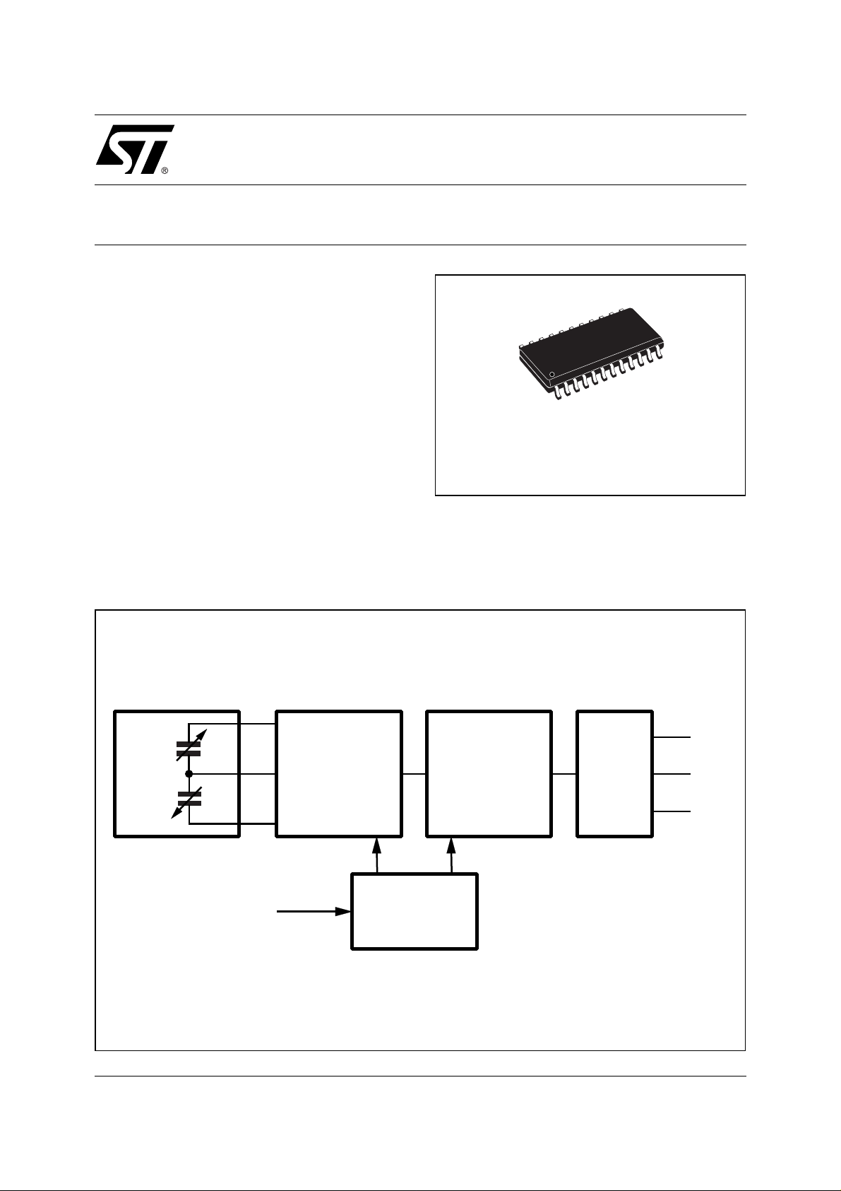
DESCRIPTION
The LIS1R02 is a complete rotational accelerometer
system based on a
Σ∆
architecture, followed by a
digital downsampling block and a digital filter, featuring high sensitivity, 800 Hz signal bandwidth and a
complete serial port interface for a direct connection
LIS1R02 (L6671)
ANGULAR ACCELEROMETER
PRODUCT PREVIEW
SO24
ORDERING NUMBER: LIS1R02
to microprocessor environment. An embedded PLL
allows internal clock generation from an external synchronization signal.
BLOCK DIAGRAM
SENSOR
A/D
CONVERTER
Clk-IN
PLL
DIGITAL
FILTER
SER.
IFC
D02IN1363
SPE
SPD
SPC
April 2002
This is preliminary information on a new product now in development. Details are subject to change without notice.
1/11
LIS1R02 (L6671)
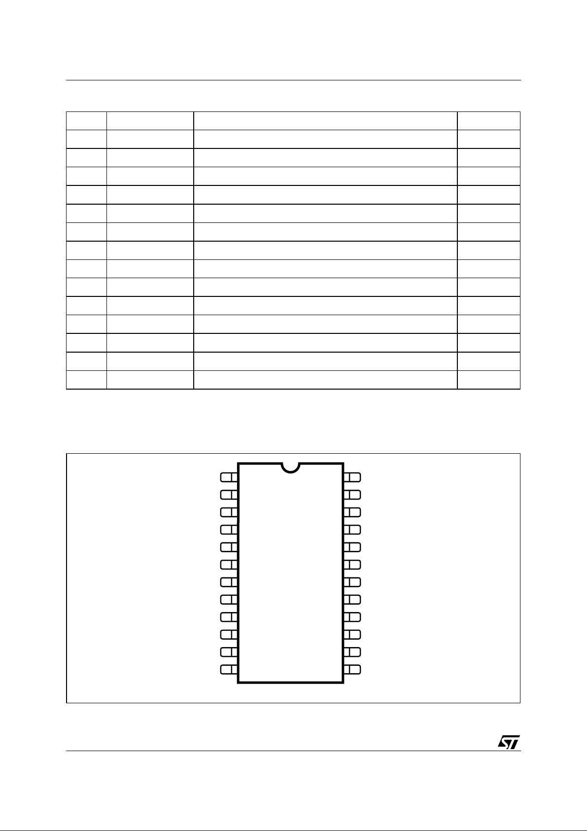
PIN FUNCTION
N°. Pin Name Function Typ. Condition
1 to 6 GND Ground
7 Vdd_Analog Analog Voltage Supply 5V Typ. (*)
8 Ref_Cap Reference Voltage Bypass
9 HV_Eprom EPROM Programming Voltage (test mode only) Tied to GND
10 Vdd_Digital Digital Voltage Supply 5V Typ. (**)
11 SPC Serial Port Clock Signal
12 SPD Serial Port Data Signal
19 to 24 GND Ground
13 SPE Serial Port Enable Signal
14 CLK_In External Clock / PLL Reference Input
15 Gnd_Digital Digital Ground Pin
16 Funct_Test Self Test
17 Test_ST Test Pin Tied to GND
18 Gnd_Analog Analog Ground Pin
(*) Must be shorted to Pin 10
(**) Must be shorted to P i n 7
PIN CONNECTIONS
(Top view)
GND
GND
GND
GND
GND
GND
_ANALOG
V
DD
REF_CAP
HV_EPROM FUNCT_TEST
V
_DIGITAL GND_DIGITAL
DD
SPC CLK_IN11 14
2
3
4
5
6
7
8
9
10
24
23
22
21
20
19
18
17
16
15
GND1
GND
GND
GND
GND
GND
GND_ANALOG
TEST_ST
2/11
1312SPD SPE
D02IN1362
LIS1R02 (L6671)
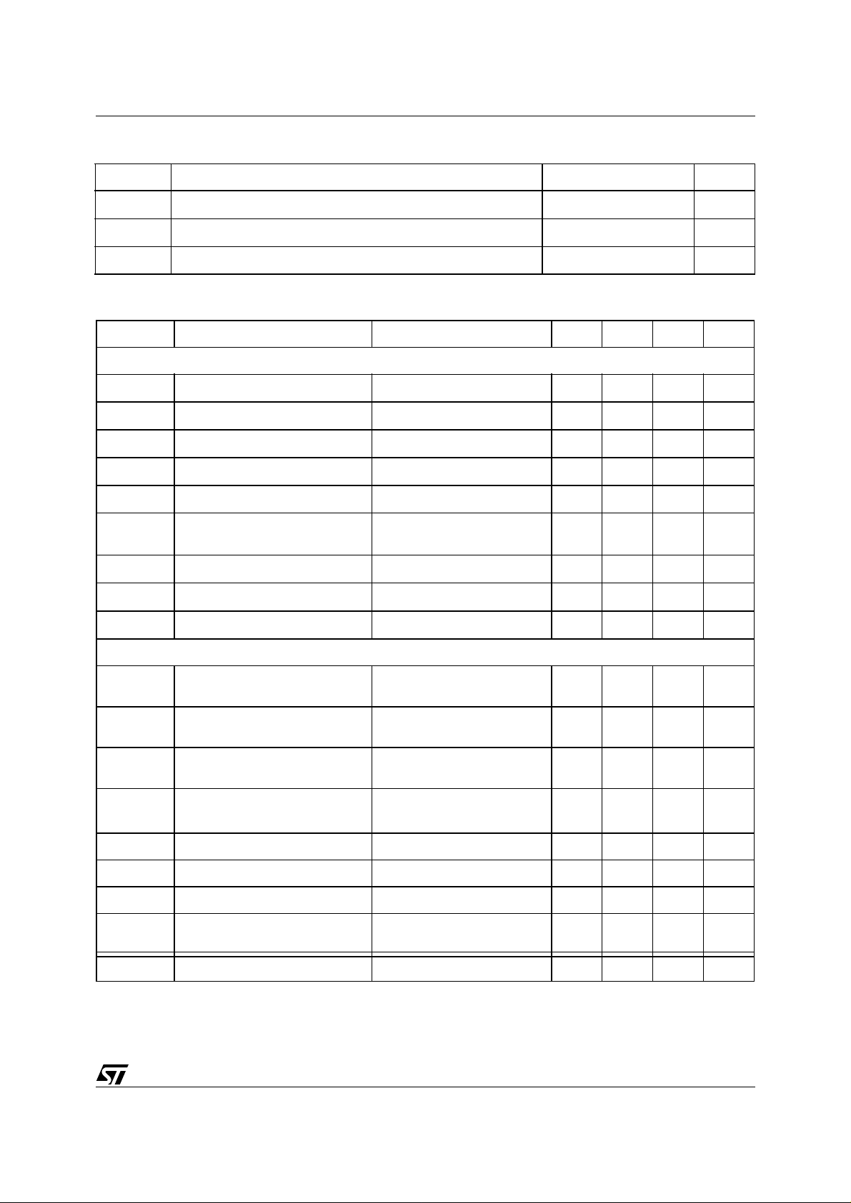
ABSOLUTE MAXIMUM RATINGS
Symbol Parameter Value Unit
Vdd
Vdd
Analog Max
Digital Max
V
in
Maximum analog supply voltage 7 V
Maximum digital supply voltage 7 V
Voltage Range on SPC, SPE, SPD, CLK_In, Funct_Test -0.3 to Vdd
Dig
+ 0.3
ELECTRICAL CHARACTERISTCS
Symbol Parameter Test Condition Min. Typ. Max. Unit
DC
Vdd
Vdd
Idd
Idd
Analog Max
Digital Max
Analog
Digital
V
ref
V
oh
V
ol
V
ih
Analog Supply Voltage 4.5 5.0 5.5 V
Digital Supply Voltage 4.5 5.0 5.5 V
Analog Circuitry Supply Current 15 mA
Digital Circuitry Supply Current 11 mA
Voltage on Ref_Cap pin 2.225 V
(on SPD and Funct_Test) @
= 3mA
I
oh
>2 V
<1 V
2.6 V
V
il
0.8 V
ADC
ADC SNR (30-800Hz, 4.48MHz
35 38 dB
Ext.Clk)
ADC SNR (30-10000Hz,
15 20 dB
4.48MHz Ext.Clk)
Phase error 30-800Hz (relative to a ref.
-30 deg
Accelerometer)
ADC Full Scale 200 rad/
ADC Bandwidth 1-800 Hz
ADC Dynamic Range 38 dB
ADC Differential Linearity <3%
ADC Integral Linearity <5% Full
Mclk Clock Frequency on CLK_In pin 6 MHz
sec
Scale
2
3/11
LIS1R02 (L6671)
SERIAL PORT TIMINGS
Symbol Parameter Test Condition Min. Typ. Max. Unit
Pin SPC
Fpc
SPC frequency 25pF maximum load Mclk 30 MHz
Pin SPE
Tec SPE to SPC 5 100 ns
Tce SPC to SPE 5 100 ns
Twe SPE low 1 SPC
Period
Pin SPD (input)
Tds SPD to SPC 5 ns
Tdh SPC to SPD 2 ne
Pin SPD (output)
Tpd SPC to SPD 10 ns
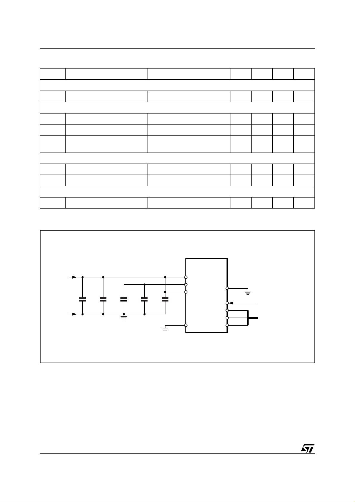
Figure 1. Application Diagram
ns
V
CC
GND
C1
22µF
6V
C2
0.22µF
C3
220pF
C4
0.22µF
C5
0.22µF
7
8
10
1 to 6
9
15 to 24
14
13
12
11
EXTERNAL CLK / PLL REF.
SPE
SPD
SPC
SERIAL I/O
D00IN1118MOD/2
4/11
 Loading...