

SINGLE J-FET OPERATIONAL AMPLIFIERS
.HIGH INPUT IMPEDANCE J-FET INPUT
STAGE
.HIGH SPEEDJ-FET OP-AMPs : up to 20MHz,
50V/µs
.OFFSETVOLTAGEADJUSTMENTDOESNOT
DEGRADEDRIFT ORCOMMON-MODE
REJECTIONAS IN MOSTOF MONOLITHIC
AMPLIFIERS
.INTERNAL COMPENSATION AND LARGE
DIFFERENTIALINPUTVOLTAGECAPABILITY
(UPTO V
TYP ICAL AP P LICATIO NS
CC
+
)
. PRECISIONHIGHSPEED INTEGRATORS
.FAST D/AANDCONVERTERS
.HIGH IMPEDANCE BUFFERS
.WIDEBAND, LOWNOISE, LOW DRIFT
AMPLIFIERS
.LOGARITHIMICAMPLIFIERS
.PHOTOCELL AMPLIFIERS
.SAMPLEANDHOLD CIRCUITS
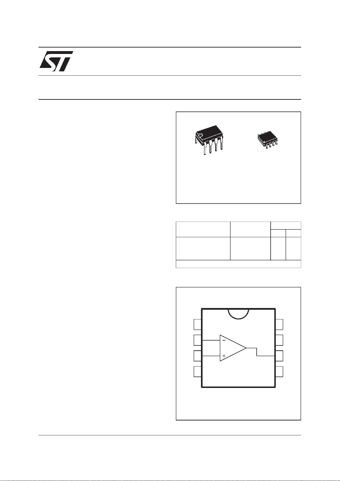
LF1 55-LF 255-L F355
LF1 56-LF 256-L F356
LF1 57-LF 257-L F357
WIDE BANDWIDTH
N
DIP8
(PlasticPackage)
ORDER CODES
Part Number
LF355, LF356, LF357 0
LF255, LF256, LF257 –40
LF155, LF156, LF157 –55
Example : LF355N
D
SO8
(PlasticMicropackage)
Temperature
Range
o
C, +70oC ••
o
C, +105oC ••
o
C, +125oC ••
Package
ND
DESC RIP TI ON
These circuits are monol i thi cJ-FETinput operational
amplifi er sincorporat i ngwell m atch ed,high voltage
J-FETonthe s amechi pwithstandardbipolartrans i s tors.
This amplifiers feature low inputbiasand offsetcurrents,low input offsetvolt ageand input offs etvoltage
drift,coupledwit hoffsetadjustwhichdoesnotdegrade
driftorcommon-moderejection.
Thedevicesarealsodesignedforhighslewrate,wide
bandwidth,extrem el yfastsettlingtim e,lowvoltageand
currentnois eand a lo w1/f nois elevel.
July1998
PIN C ONNEC TI ONS (top v iew)
1
2
3
4
1 - Offset Null 1
2 - Inverting input
3 - Non-inverting input
-
4-V
CC
5 - Offset Null 2
6 - Output
7-V
8 - N.C.
CC
8
7
6
5
+
1/14
LF155 - LF156 - LF157
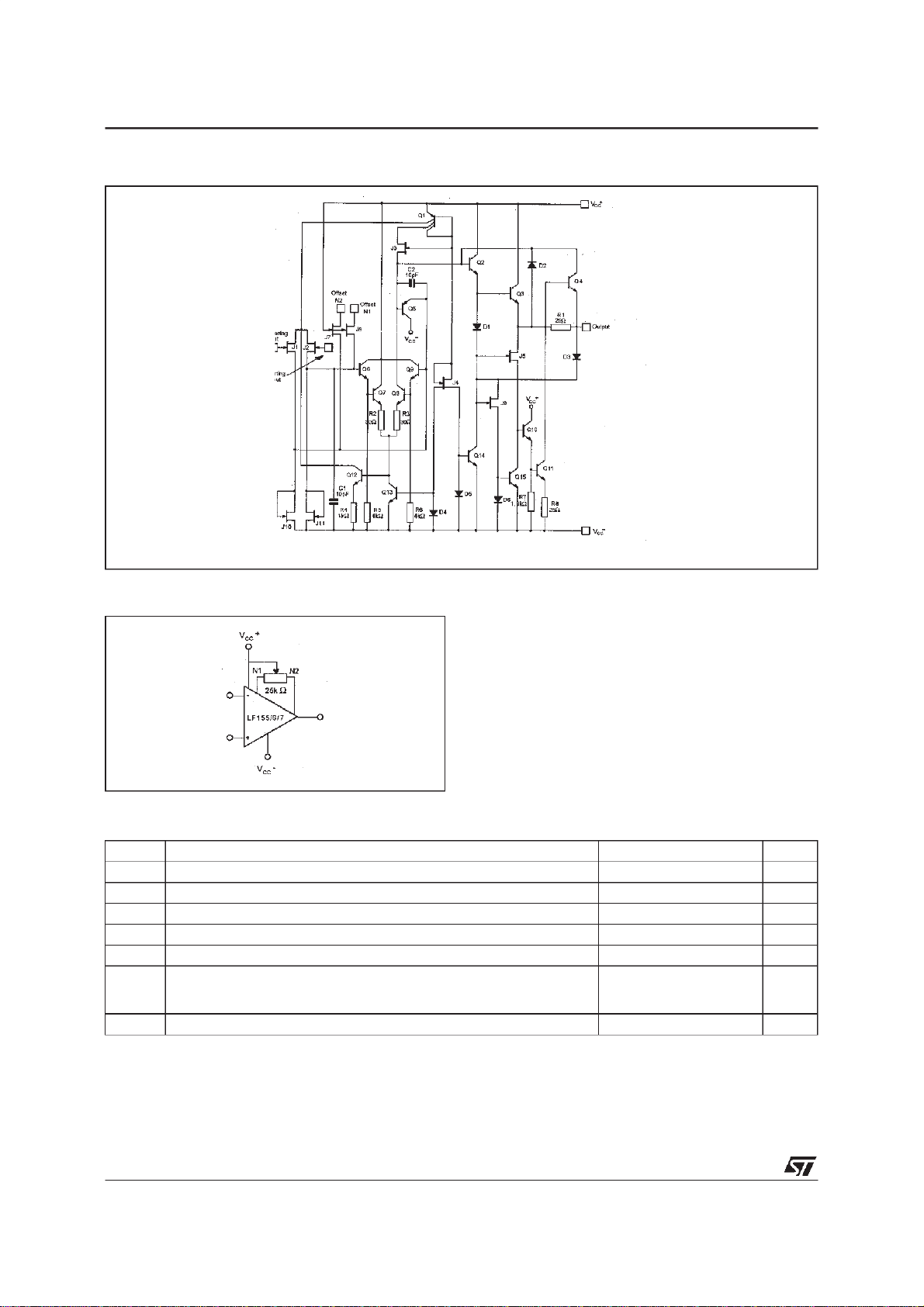
SCHE MATIC DIAGRAM
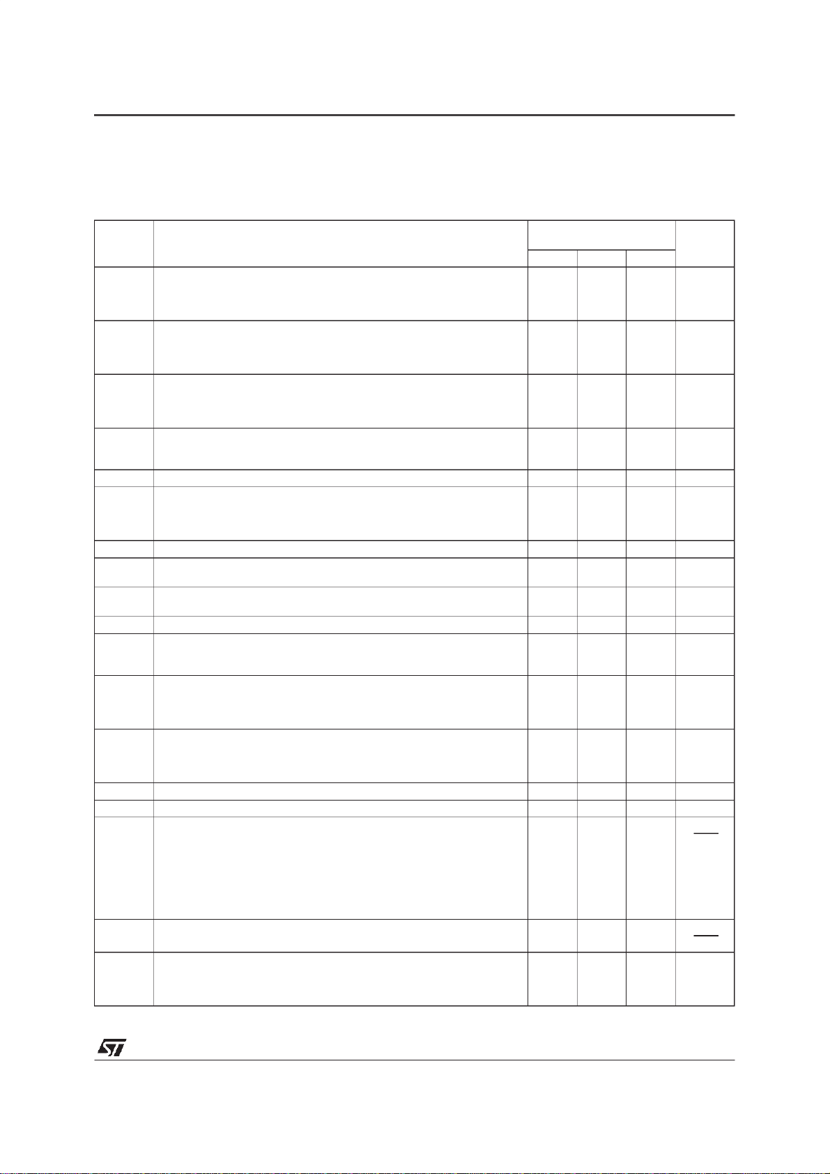
ADJUSTMENT
V
io
ABSOLUTE MAXIMUM RATINGS
Symbol Parameter Value Unit
V
P
T
T
Supply Voltage ±22 V
CC
Input Voltage - (note 1) ±20 V
V
i
Differential Input Voltage ±40 V
V
id
Power Dissipation 570 mW
tot
Output Short-circuit Duration Infinite
Operating Free Air Temperature Range LF155-LF156-LF157
oper
LF255-LF256-LF257
LF355-LF356-LF357
Storage Temperature Range –65 to 150
stg
-55 to +125
–40 to +105
0to70
o
C
o
C
2/14
LF155 - LF156 - LF157
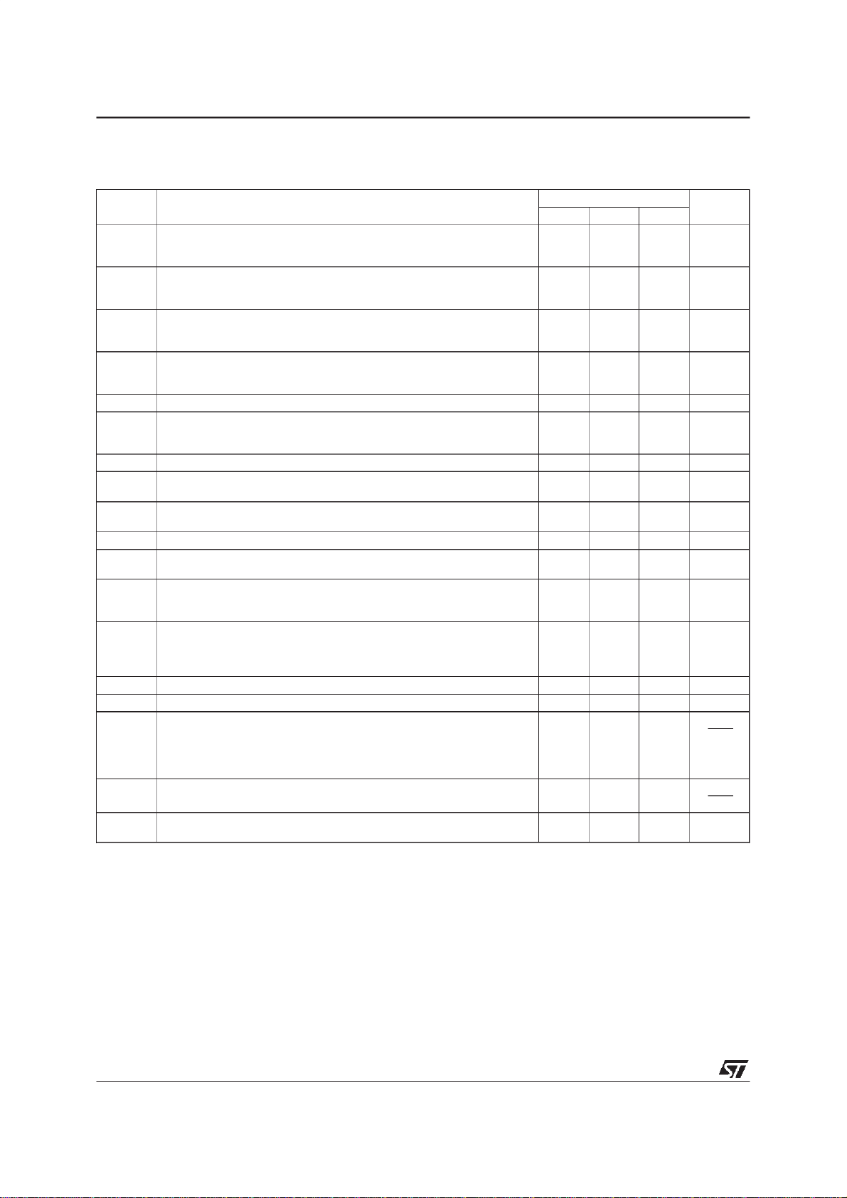
ELECTRICAL CHARACTERISTICS
LF155, LF156, LF157 -55
LF255, LF256, LF257 -40
o
C ≤ T
o
C ≤ T
≤ +125oC ±5V ≤ VCC≤ ±20V
amb
≤ +105oC ±5V ≤ VCC≤ ±20V
amb
(unless otherwise specified)
LF155 - LF156 - LF157
Symbol Parameter
V
A
Input Offset Voltage (RS=50Ω)
io
Input Offset Current - (note 3)
I
io
Input Bias Current - (note 3)
I
ib
Large Signal Voltage Gain (RL=2kΩ,VO=±10V, VCC= ±15V)
vd
T
T
T
T
T
T
T
T
amb
min.
amb
min.
amb
min.
amb
min.
=25oC
≤ T
amb
=25oC
≤ T
amb
=25oC
≤ T
amb
=25oC
≤ T
amb
≤ T
≤ T
≤ T
≤ T
max.
max.
max.
max.
LF155, LF156, LF157
LF255, LF256, LF257
LF155, LF156, LF157
LF255, LF256, LF257
LF155, LF156, LF157
LF255, LF256, LF257
SVR Supply Voltage Rejection Ratio - (note 4) 85 100 dB
I
Supply Current (VCC= ±15V, no load)
CC
=25oC LF155, LF255
T
amb
LF156, LF256
LF157, LF257
DV
DV
V
Input Offset Voltage Drift (RS=50Ω)5µV/oC
io
Change in Average Temperature Coefficient with Vioadjust
io/Vio
icm
=50Ω) - (note 2)
(R
S
Input Common Mode Voltage Range (VCC= ±15V, T
=25oC) ±11 +15.1
amb
CMR Common Mode Rejection Ratio 85 100 dB
±V
GBP Gain Bandwidth Product (V
Output Voltage Swing (VCC= ±15V)
OPP
R
L
R
L
= 10kΩ
=2kΩ
= ±15V, T
CC
=25oC)
amb
LF155, LF255
LF156, LF256
LF157, LF257
SR Slew Rate (V
= 1 LF155, LF255
A
V
= 5 LF157, LF257
A
V
Input Resistance (T
R
i
C
Input Capacitance (VCC= ±15V, T
i
e
Equivalent Input Noise Voltage
n
= ±15V, T
(V
CC
f = 1000Hz LF155, LF255
= ±15V, T
CC
amb
=25oC, RS= 100Ω)
amb
=25oC)
amb
LF156, LF256
=25oC) 10
=25oC) 3 pF
amb
LF156, LF256
LF157, LF257
f = 100Hz LF155, LF255
LF156, LF256
LF157, LF257
Equivalent Input Noise Current
i
n
t
s
(V
CC
= ±15V, T
=25oC, f = 100Hz or f = 1000Hz)
amb
Settling Time (VCC= ±15V, T
=25oC) - (note 5)
amb
LF155, LF255
LF156, LF256
LF157, LF257
LF255 - LF256 - LF257
Min. Typ. Max.
35
7
6.2
320
20
1
20 100
50
5
50
200
25
2
5
5
4
7
7
0.5 µV/
-12
±12
±10
±13
±12
2.5
5
20
5
7.5
30
12
50
12
20
12
12
25
15
15
0.01
4
1.5
1.5
Unit
mV
pA
nA
nA
pA
nA
nA
V/mV
mA
o
V
V
MHz
V/µs
Ω
nV
√Hz
pA
√Hz
µs
C
3/14
LF155 - LF156 - LF157
ELECTRICAL CHARACTERISTICS
LF355, LF356, LF357 0
Symbol Parameter
V
A
Input Offset Voltage (RS=50Ω)
io
Input Offset Current - (note 3)
I
io
Input Bias Current - (note 3)
I
ib
Large Signal Voltage Gain (RL=2kΩ,VO=±10V)
vd
T
T
T
T
T
T
T
T
amb
min.
amb
min.
amb
min.
amb
min.
=25oC
≤ T
amb
=25oC
≤ T
amb
=25oC
≤ T
amb
=25oC
≤ T
amb
≤ T
≤ T
≤ T
≤ T
max.
max.
max.
max.
o
C ≤ T
≤ +70oCV
amb
CC
= ±15V
, (unless otherwise specified)
LF355 - LF356 - LF357
Min. Typ. Max.
310
350
20 200
25
200
15
13
2pAnA
8
SVR Supply Voltage Rejection Ratio - (note 4) 80 100 dB
I
DV
DV
V
Supply Current (no load)
CC
Input Offset Voltage Drift (RS=50Ω) - (note 2) 5 µV/oC
io
Change in Average Temperature Coefficient with Vioadjust
io/Vio
(R
Input Common Mode Voltage Range (T
icm
=25oC LF355
T
amb
=50Ω)
S
LF356, LF357
=25oC) ±10 +15.1
amb
2
5
0.5 µV/
-12
4
10
CMR Common Mode Rejection Ratio 80 100 dB
±V
Output Voltage Swing RL= 10kΩ
OPP
GBP Gain Bandwidth Product T
=25oC) LF355
amb
=2kΩ
R
L
LF356
±12
±10
LF357
SR Slew Rate (T
= 1 LF355
A
V
= 5 LF357
A
V
Input Resistance (T
R
i
C
Input Capacitance (Tamb = 25oC) 3 pF
i
e
Equivalent Input Noise Voltage (T
n
f = 1000Hz LF355
amb
=25oC)
LF356
=25oC) 10
amb
=25oC, RS= 100Ω)
amb
LF356, LF357
f = 100Hz LF355
LF356, LF357
Equivalent Input Noise Current
i
n
t
s
Notes: 1. Unless otherwise specified the absolute maximumnegative inputvoltage is equaltothe negative power supply voltage.
2. The temperaturecoefficient of the adjustedinput offset voltage changes only a small amount(0.5µV/
3. The input bias currents are junctionleakage currents which approximately double for every 10
4. Supply voltage rejection is measured for both supply magnitudesincreasing or decreasing simultaneously, inaccordance with
5. Settling time is defined here,fora unitygain inverter connection using 2kΩ resistorsfor the LF155, LF156 series. It is the time
=25oC, f = 100Hz or f = 1000Hz)
(T
amb
Settling Time (T
of adjustment fromits original unadjusted value. Common-mode rejection and open loop voltagegainare alsounaffected by
offsetadjustment.
temperature T
In anormaloperation the junction temperature rises above the ambienttemperature as a result of internal powerdissipation,
P
tot-Tamb=Tamb+Rth(j-a)xPtot
f input currents areto bekept to aminimum.
common practise.
required for the errorvoltage (the voltage atthe invertinginput pinon theamplifier) to settleto within0.01%ofits final value from
the time a 10V step inputis applied to theinverter. For the LF157 seriesA
and the outputstep is 10V.
amb
=25oC) - (note 5) LF355
amb
. Dueto limited production test time, the input bias currentmeasured is correlatedto junction temperature.
where Rt
is the thermal resistance from junction to ambient. Use ofa heatsink is recommended
h(j-a)
LF356, LF357
= -5, thefeedback resistor from output to inputis 2kΩ
V
±13
±12
2.5
5
20
5
12
50
12
20
12
25
15
0.01
4
1.5
o
C typically) for each mV
o
C increase in thejunction
Unit
mV
pA
nA
V/mV
mA
o
C
per mV
V
V
MHz
V/µs
Ω
nV
√Hz
pA
√Hz
µs
4/14

APPL ICATION HINTS
The LF155, LF156,LF157seri esareopamps withJFETinputtrans i sto r s .TheseJF E Tshavelargereverse
breakdownvoltagesfr om gat etosourceor drain elim i natingtheneedofclampsacrossthe inputs.Therefore
large differ enti alinput voltagescan easily be accommodatedwithoutalargeincreaseofinputcur re nt s.The
maximumdifferentialinput voltage is independentof
thesupplyvoltage.However,neitherofthenegativ einput vol tages s houl dbe allowedto exceedthenegative
supplyas this will caus elarge curre ntsto flow which
canresultin adestroyedunit.Exceedi ngthe negat i v e
common-modelim i toneitherinp utw i l lcauseareversal
of thephasetotheoutputandforcethe ampli fi eroutput
to the correspondi nghi gh or lowstate . Exceedingthe
negativecommon-mo delimit on bothinputs will force
theamplifieroutputtoahighstate.Inneithercasedoes
a latch occur since raising the input back within the
common-moderangeagain putstheinput stageand
thustheamplifi erin anormaloperatingmode.Exceedingthepositi vecom mon-modelim i tonasingleinputwil l
not ch angethephaseoftheoutputhowever ,ifbothinputsexceedthelimi t, theoutputof theamplifier will be
forcedtoahighstate.Theseampli fi erswilloperat ewith
the common-m odeinputvoltageequal tothe positi v e
supply. In fact, the common-modevol tagec anex ceedthepositiv esupplybyapproximately100mVindependentof supply volt-age and over thefull operatingtemperatur erange.The positive suplly can thereforebeusedasa referenceonaninputas,forexam ple,
in asupplycurr entmonitorand/orlimiter .Prec auti ons shouldbetakentoensurethatthepowersupplyforthe
integratedcircuitneverbecomesre-versedin polarity
orthattheunitisnot inadvertentlyin- st al l edbackwar ds
LF155 - LF156 - LF157
in a socket as an unilim i tedcurrentsurge throu ghthe
resul ti ngforwarddiodewithi ntheIC coul dcausefusi ngoftheinternalconductors andresul tinadestroy eduni t.
Becausethese amplifi ersareJFETratherthan MOS FET inputop ampstheydo not requirespecialhandling.
AllofthebiascurrentsintheseamplifiersaresetbyFET
currentsources. The draincurrentsforthe amplifiers
are therefore essenti al l y independentof supply volt ages.
Aswithmostam pl i f i er s ,careshouldbetakenwithlead
dress,c om ponentsplacemen tandsupplydecoupling
inordertoensurestability.Forexample,resi storsfrom
theoutputtoan inputshouldbe placedwith thebody
closetothei nputtominim iz”pickup”andmaximiz ethe
frequencyof the feedbackpole bymini mizing the capacitancefromthe input to ground.
A feedbackpole is creat edw henthe feedbackaround
any amplifier is resistive. The parallel resistance and
capacitanc efromtheinput of thedevice(usual l ythe inverting input)toacgrounds etthefrequenc y ofthepole.In
many instanc es the frequency of this pole is muc h
greaterthantheexpected3dBfrequencyof the closed
loopgainandconsequentlythereisnegligi bleeffect on
stability margin. However, if the feedback pole is less
than approximately six time the expected3 dB frequencyaleadcapaci t orshouldbeplacedfromtheoutputtothe inputoftheop amp.Thevalueof that added
capacitorshouldbesuchthatthe RC tim econs tantof
thiscapacitorand theresistanceitparallelsisgreater
than or equal to theoriginal feedbackpoletime constant.
5/14
 Loading...