

Ldmos Enhanced Technology in Plastic Package
Designed for GSM / EDGE / IS-97 / WCDMA
applications
• EXCELLENT THERMAL STABILITY
• COMMON SOURCE CONFIGURATION
• P
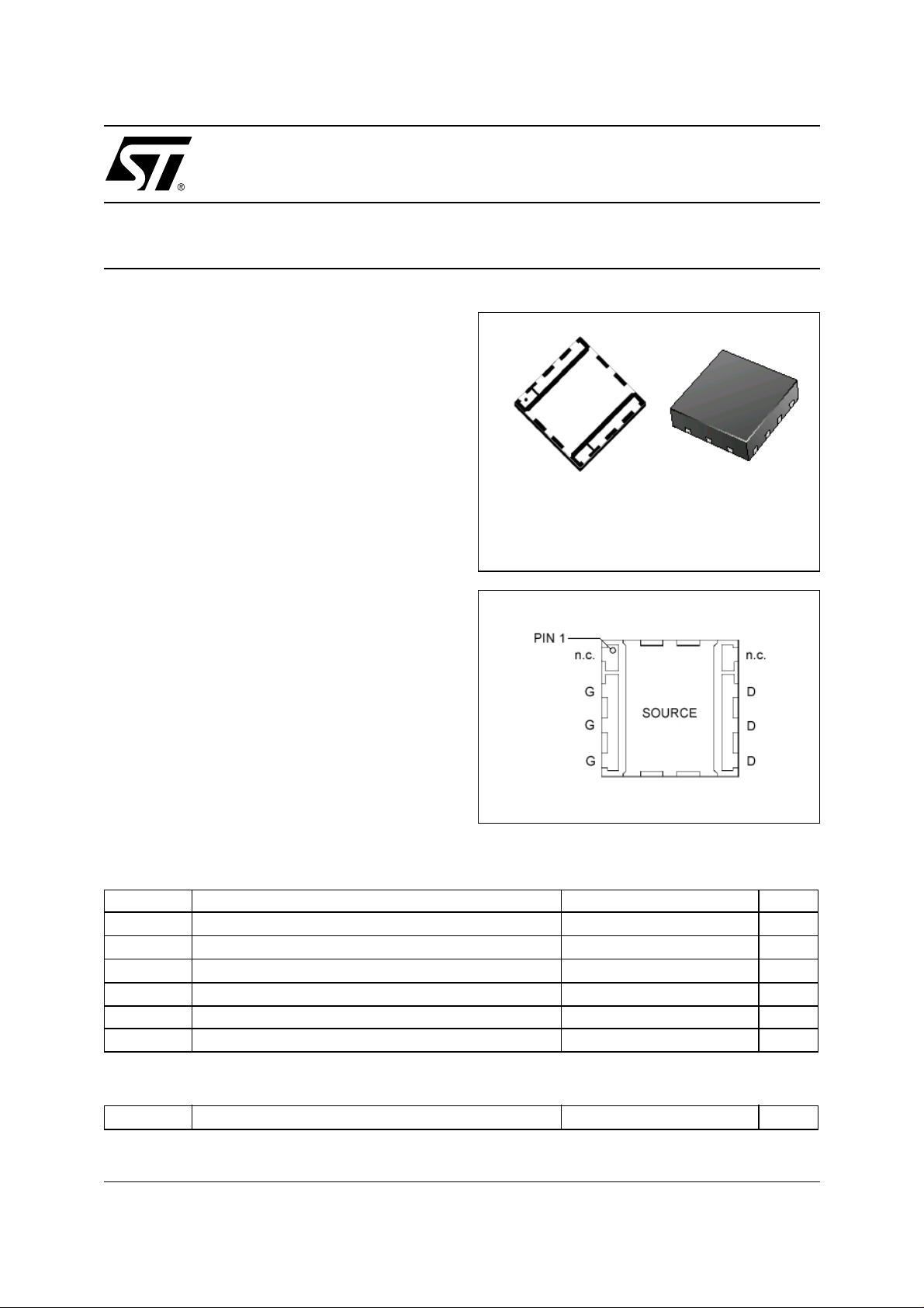
• NEW LEADLESS PLASTIC PACKAGE
• ESD PROTECTIO N
= 8 W with 11 dB gain @ 2170 MHz / 26V
OUT
LET21008
RF POWER TRANSISTORS
TARGET DATA
PowerFLAT
ORDER CODE
LET21008
™(5x5)
BRANDING
21008
DESCRIPTION
The LET21008 is a comm on source N-Channel,
enhancement-mode lateral Field-Effect RF power
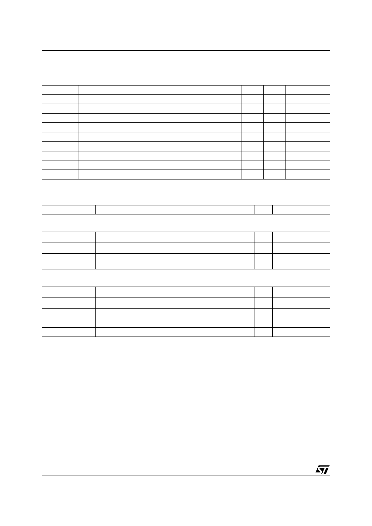
PIN CONNECTION
transistor. It is designed for high gain, broad band
commercial and industrial applications. It operates
at 26 V in common source mode at frequencies up
to 2.1 GHz. LET21008 boasts the excellent gain,
linearity and reliability of ST’s latest LDMOS
technology mounted in the innovative leadless
SMD plastic package, PowerFLAT™.
LET21008’s superior linearity performance makes
it an ideal solution for base station applica-
tions .
TOP VIEW
ABSOLUTE MAXIMUM RATINGS (T
Symbol Parameter Value Unit
V
(BR)DSS
V
GS
I
D
P
DISS
Tj Max. Operating Junction Temperature 150 °C
T
STG
Drain-Source Voltage 65 V
Gate-Source Voltage -0.5 to +15 V
Drain Current 2.0 A
Power Dissipation (@ Tc = 70°C) TBD W
Storage Temperature -65 to +150 °C
CASE
= 25 °C)
THERMA L D ATA
R
th(j-c)
April, 15 2003
Junction -Case Thermal Resistance TBD °C/W
1/4
LET21008
ELECTRICAL SPECIFICATION (T
CASE
= 25 °C)
STATIC
Symbol Test Conditions Min. Typ. Max. Unit
V
(BR)DSS
I
DSS
I
GSS
V
GS(Q)
V
DS(ON)
G
C
ISS
C
OSS
C
RSS
FS
VGS = 0 V IDS = 1 mA
VGS = 0 V VDS = 26 V
VGS = 5 V VDS = 0 V
VDS = 26 V
ID
= TBD
VGS = 10 V ID = 1 A
VDS = 10 V ID = 1 A
VGS = 0 V VDS = 26 V f = 1 MHz
VGS = 0 V VDS = 26 V f = 1 MHz
VGS = 0 V VDS = 26 V f = 1 MHz
65 V
1 µA
1 µA
2.5 5.0 V
TBD V
TBD mho
TBD pF
TBD pF
TBD pF
Symbol Test Conditions Min. Typ. Max. Unit
DYNAMIC (
mismatch
P
η
Load
OUT
D
(1)
(1)
f = 2170 MHz
VDD = 26 V IDQ = TBD
VDD = 26 V IDQ = TBD
= 26 V P
V
DD
ALL PHASE ANGLES
)
12 15 W
45 50 %
= 8 W
OUT
20:1 VSWR
DYNAMIC (
P
OUT(W-CDMA)
η
D(W-CDMA)
(1) 1 dB Compression point
f = 2110 - 2170 MHz
(1)
P
OUT
(1)
η
D
G
P
)
VDD = 26 V IDQ = TBD
VDD = 26 V IDQ = TBD
VDD = 26 V IDQ = TBD P
OUT
= 8 W
ACPR -45 dBc 2.5 W
ACPR -45 dBc 25 %
8W
40 45 %
11 13 dB
2/4
 Loading...