

SGS Thomson Microelectronics LE80CZ, LE80CD, LE60CZ, LE60CD, LE60ABZ Datasheet
...
LE00AB/C
SERIES
VERY LOW DROP
VOLTAGE REGULATORS WITH INHIBIT
September 1998
■ VERYLOWDROPOUTVOLTAGE(0.2VTYP.)
■ VERYLOW QUIESCENTCURRENT
(TYP.50µA IN OFFMODE, 0.5mAINON
MODE, NO LOAD)
■ OUTPUTCURRENT UPTO100mA
■ OUTPUTVOLTAGESOF 1.25; 1.5; 2.5; 2.7; 3;
3.3; 3.5;4;4.5; 4.7; 5;5.2; 5.5; 6; 8V
■ INTERNALCURRENT AND THERMALLIMIT
■ ONLY2.2µF FORSTABILITY
■ AVAILABLEIN ± 1% (A) OR ± 2%(C)
SELECTIONAT 25
o
C
■ SUPPLYVOLTAGEREJECTION:80 db (TYP.)
■ TEMPERATURERANGE:-40 TO 125
o
C
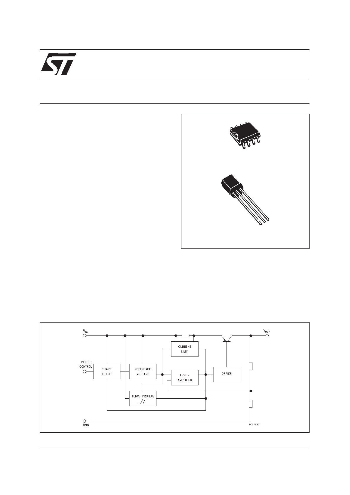
DESCRIPTION
The LE00 regulator series are very Low Drop
regulatorsavailablein SO-8and TO-92packages
and in a wide range of outputvoltages.
The very Low Drop voltage (0.2V) and the very
low quiescent current make them particularly
suitable for Low Noise Low Power applications
and speciallyin battery powered systems.
They are pin to pin compatible with the older
L78L00 series. Furthermore in the 8 pin
configuration (SO-8) they employ a Shutdown
Logic Control (pin 5, TTL compatible). This
means that when the device is used as a local
regulator, it’s possible to put in stand by a part of
the board even more decreasing the total power
consumption. In the three terminal configuration
(TO-92) the device is even in ON STATE,
mantaining the same electrical performances. It
needs only 2.2µF capacitor for stability allowing
room and cost savingeffect.
SCHEMATICDIAGRAM
SO-8
TO-92
1/25
ABSOLUTE MAXIMUM RATING
Symbol Parameter Value Unit
V
i
DC InputVoltage 20 V
I
o
OutputCurrent Internally limited (*)
P
tot
Power Dissipation Internally limited (*)
T
stg
StorageTemperature Range - 40 to 150
o
C
T
op
OperatingJunction Temperature Range - 40 to 125
o
C
(*) Our SO-8package used for Voltage Regulatorsis modified internally to have pins 2, 3, 6and 7 electricallycommoned tothe dieattach
flag.This particular frame decreases thetotal thermal resistance of the package and increases its ability to dissipatepower when an
appropriatearea of copper on the printedcircuit board is available for heatsinking. The external dimensions are the same as for the
standard SO-8
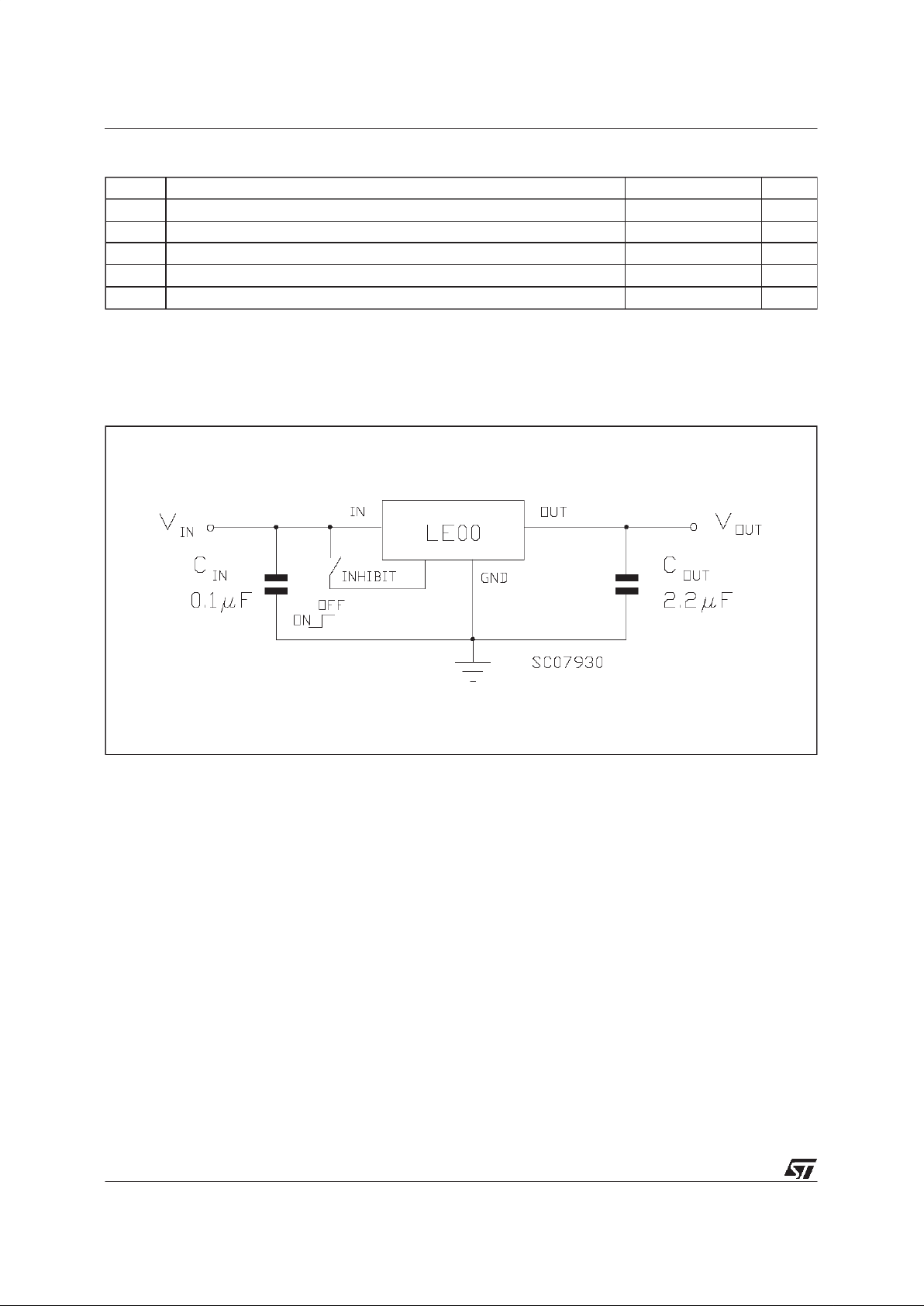
TEST CIRCUITS
Note: If theInhibit pin is left floating, the regualtor is inON mode. However, to avoid any noise picking-up, it is suggestedto ground it when
LE00AB/C
2/25
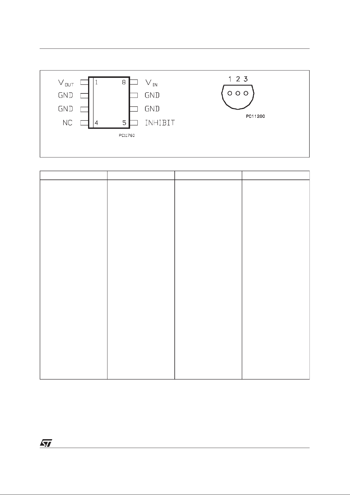
CONNECTIONDIAGRAMAND ORDERING NUMBERS (top view)
ORDERING NUMBERS
Type SO-8 TO-92 Output Voltage
LE12AB
LE12C
LE15AB
LE15C
LE25AB
LE25C
LE27AB
LE27C
LE30AB
LE30C
LE33AB
LE33C
LE35AB
LE35C
LE40AB
LE40C
LE45AB
LE45C
LE47AB
LE47C
LE50AB
LE50C
LE52AB
LE52C
LE55AB
LE55C
LE60AB(*)
LE60C(*)
LE80AB(*)
LE80C(*)
LE120AB(*)
LE120C(*)
LE12ABD
LE12CD
LE15ABD
LE15CD
LE25ABD
LE25CD
LE27ABD
LE27CD
LE30ABD
LE30CD
LE33ABD
LE33CD
LE35ABD
LE35CD
LE40ABD
LE40CD
LE45ABD
LE45CD
LE47ABD
LE47CD
LE50ABD
LE50CD
LE52ABD
LE52CD
LE55ABD
LE55CD
LE60ABD
LE60CD
LE80ABD
LE80CD
LE120ABD
LE120CD
LE12ABZ
LE12CZ
LE15ABZ
LE15CZ
LE25ABZ
LE25CZ
LE27ABZ
LE27CZ
LE30ABZ
LE30CZ
LE33ABZ
LE33CZ
LE35ABZ
LE35CZ
LE40ABZ
LE40CZ
LE45ABZ
LE45CZ
LE47ABZ
LE47CZ
LE50ABZ
LE50CZ
LE52ABZ
LE52CZ
LE55ABZ
LE55CZ
LE60ABZ
LE60CZ
LE80ABZ
LE80CZ
LE120ABZ
LE120CZ
1.25 V
1.25 V
1.5 V
1.5 V
2.5 V
2.5 V
2.7 V
2.7 V
3V
3V
3.3 V
3.3 V
3.5 V
3.5 V
4V
4V
4.5 V
4.5 V
4.7 V
4.7 V
5V
5V
5.2 V
5.2 V
5.5 V
5.5 V
6V
6V
8V
8V
12 V
12 V
(*) Available onrequest
SO-8 TO-92
pin 1 = OUT
pin 2 =GND
pin 3 = IN
BOTTOM VIEW
LE00AB/C
3/25
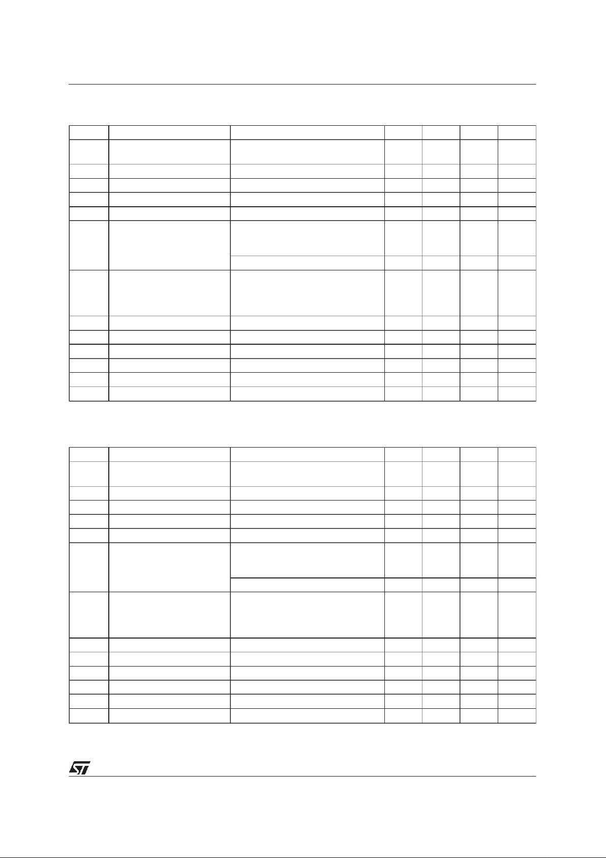
ELECTRICALCHARACTERISTICS FOR LE12AB (refer to the test circuits, Tj=25oC,
C
i
=0.1 µF, Co= 2.2 µFunlessotherwise specified)
Symbol Parameter Test Conditions Min. Typ. Max. Unit
V
o
OutputVoltage Io= 10 mA, Vi=3.3 V
I
o
= 10 mA, Vi=3.3 V -25<Ta<85oC
1.225
1.2
1.25 1.275
1.3
V
V
V
i
OperatingInputVoltage Io= 100mA 2.5 18 V
I
out
OutputCurrent Limit 150 mA
∆V
o
LineRegulation Vi=2.5to 18 V, Io=0.5 mA 3 15 mV
∆V
o
LoadRegulation Vi=2.8V Io=0.5to 100 mA 3 15 mV
I
d
Quiescent Current ON MODE
V
i
=2.5to 18 V Io=0 mA
V
i
=2.5to 18 V Io=100 mA
0.5
1.5
1
3
mA
mA
OFF MODE V
i
= 6V 50 100 µA
SVR Supply VoltageRejection
I
o
= 5mA Vi= 3.5V ± 1V
f = 120Hz
f = 1 KHz
f = 10 KHz
82
77
60
dB
dB
dB
eN OutputNoise Voltage B = 10 Hzto 100 KHz 50 µV
V
d
DropoutVoltage Io= 100mA -40< Ta< 125oC1.25V
V
il
ControlInput Logic Low -40 < Ta<125oC0.8V
V
ih
ControlInput Logic High -40 < Ta<125oC2 V
I
i
ControlInput Current Vi=6 V, Vc=6V 10 µA
C
O
OutputBypass Capacitance
ESR =0.1 to 10 Ω I
o
=0 to 100 mA
210 µF
ELECTRICALCHARACTERISTICS FOR LE12C (refer to the test circuits, Tj=25oC,
C
i
=0.1 µF, Co= 2.2 µFunlessotherwise specified)
Symbol Parameter Test Conditions Min. Typ. Max. Unit
V
o
OutputVoltage Io= 10 mA, Vi=3.3 V
I
o
= 10 mA, Vi=3.3 V -25<Ta<85oC
1.225
1.2
1.25 1.275
1.3
V
V
V
i
OperatingInputVoltage Io= 100mA 2.5 18 V
I
out
OutputCurrent Limit 150 mA
∆V
o
LineRegulation Vi=2.5to 18 V, Io=0.5 mA 3 20 mV
∆V
o
LoadRegulation Vi=2.8V Io=0.5to 100 mA 3 25 mV
I
d
Quiescent Current ON MODE
V
i
=2.5to 18 V Io=0 mA
V
i
=2.5to 18 V Io=100 mA
0.5
1.5
1
3
mA
mA
OFF MODE V
i
= 6V 50 100 µA
SVR Supply VoltageRejection
I
o
= 5mA Vi= 3.5V ± 1V
f = 120Hz
f = 1 KHz
f = 10 KHz
82
77
60
dB
dB
dB
eN OutputNoise Voltage B = 10 Hzto 100 KHz 50 µV
V
d
DropoutVoltage Io= 100mA -40< Ta< 125oC1.25V
V
il
ControlInput Logic Low -40 < Ta<125oC0.8V
V
ih
ControlInput Logic High -40 < Ta<125oC2 V
I
i
ControlInput Current Vi=6 V, Vc=6V 10 µA
C
O
OutputBypass Capacitance
ESR =0.1 to 10 Ω I
o
=0 to 100 mA
210 µF
LE00AB/C
4/25
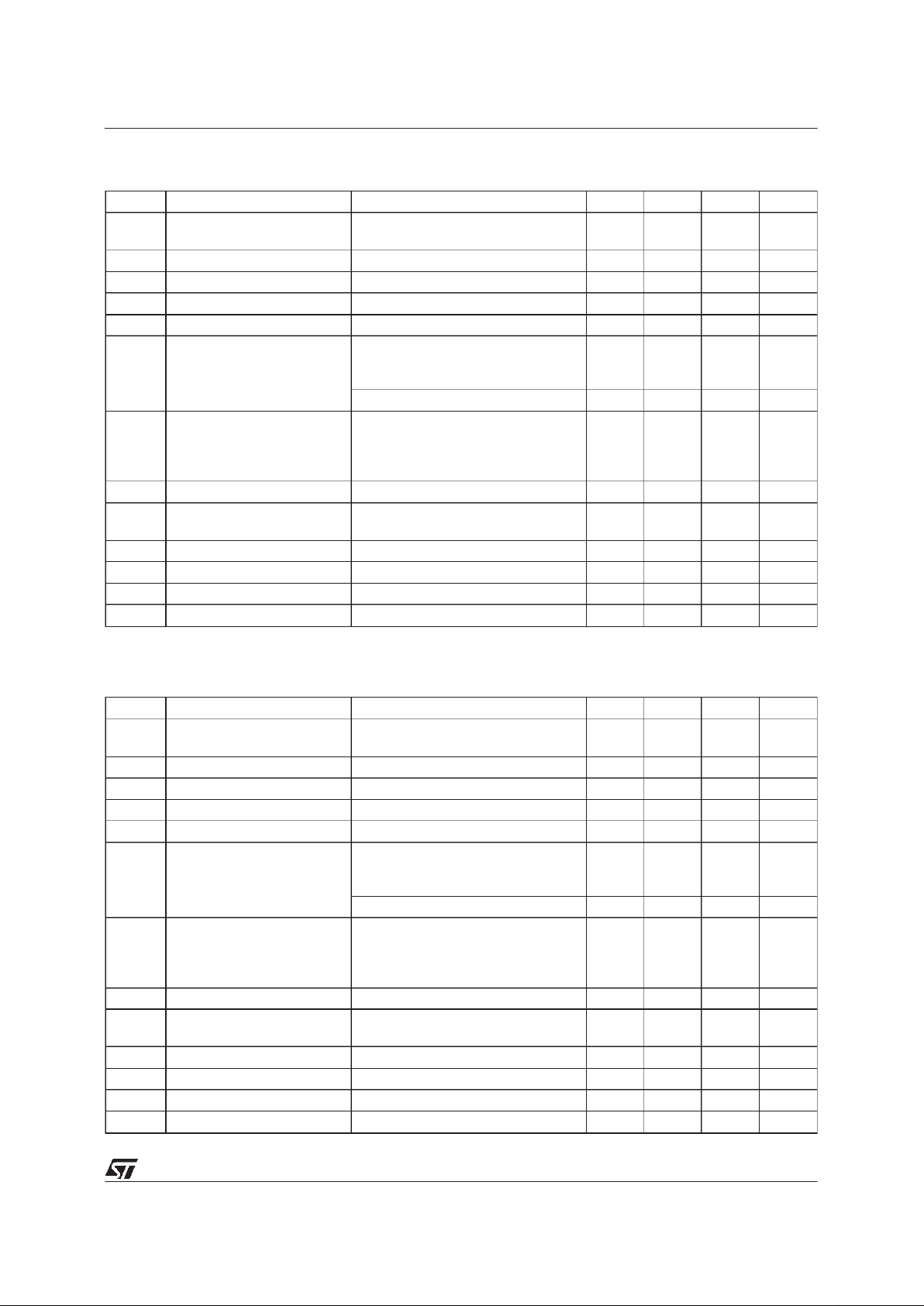
ELECTRICALCHARACTERISTICS FOR LE15AB (refer to the test circuits, Tj=25oC,
C
i
=0.1 µF, Co= 2.2 µFunlessotherwise specified)
Symbol Parameter Test Conditions Min. Typ. Max. Unit
V
o
OutputVoltage Io= 10 mA, Vi=3.5 V
I
o
= 10 mA, Vi=3.5 V -25<Ta<85oC
1.47
1.44
1.5 1.53
1.56
V
V
V
i
OperatingInputVoltage Io= 100mA 2.5 18 V
I
out
OutputCurrent Limit 150 mA
∆V
o
LineRegulation Vi=2.5to 18 V, Io=0.5 mA 3 15 mV
∆V
o
LoadRegulation Vi=2.8V Io=0.5to 100 mA 3 15 mV
I
d
Quiescent Current ON MODE
V
i
=2.5to 18 V Io=0 mA
V
i
=2.5to 18 V Io=100 mA
0.5
1.5
1
3
mA
mA
OFF MODE V
i
= 6V 50 100 µA
SVR Supply VoltageRejection
I
o
= 5mA Vi= 3.5V ± 1V
f = 120Hz
f = 1 KHz
f = 10 KHz
82
77
60
dB
dB
dB
eN OutputNoise Voltage B = 10 Hzto 100 KHz 50 µV
V
d
DropoutVoltage Io= 100mA -40< Ta< 125oC1V
V
il
ControlInput Logic Low -40 < Ta<125oC0.8V
V
ih
ControlInput Logic High -40 < Ta<125oC2 V
I
i
ControlInput Current Vi=6 V, Vc=6V 10 µA
C
O
OutputBypass Capacitance
ESR =0.1 to 10 Ω I
o
=0 to 100 mA
210 µF
ELECTRICALCHARACTERISTICS FOR LE15C (refer to the test circuits, Tj=25oC,
C
i
=0.1 µF, Co= 2.2 µFunlessotherwise specified)
Symbol Parameter Test Conditions Min. Typ. Max. Unit
V
o
OutputVoltage Io= 10 mA, Vi=3.5 V
I
o
= 10 mA, Vi=3.5 V -25<Ta<85oC
1.47
1.44
1.5 1.53
1.56
V
V
V
i
OperatingInputVoltage Io= 100mA 2.5 18 V
I
out
OutputCurrent Limit 150 mA
∆V
o
LineRegulation Vi=2.5to 18 V, Io=0.5 mA 3 20 mV
∆V
o
LoadRegulation Vi=2.8V Io=0.5to 100 mA 3 25 mV
I
d
Quiescent Current ON MODE
V
i
=2.5to 18 V Io=0 mA
V
i
=2.5to 18 V Io=100 mA
0.5
1.5
1
3
mA
mA
OFF MODE V
i
= 6V 50 100 µA
SVR Supply VoltageRejection
I
o
= 5mA Vi= 3.5V ± 1V
f = 120Hz
f = 1 KHz
f = 10 KHz
82
77
60
dB
dB
dB
eN OutputNoise Voltage B = 10 Hzto 100 KHz 50 µV
V
d
DropoutVoltage Io= 100mA -40< Ta< 125oC1V
V
il
ControlInput Logic Low -40 < Ta<125oC0.8V
V
ih
ControlInput Logic High -40 < Ta<125oC2 V
I
i
ControlInput Current Vi=6 V, Vc=6V 10 µA
C
O
OutputBypass Capacitance
ESR =0.1 to 10 Ω I
o
=0 to 100 mA
210 µF
LE00AB/C
5/25

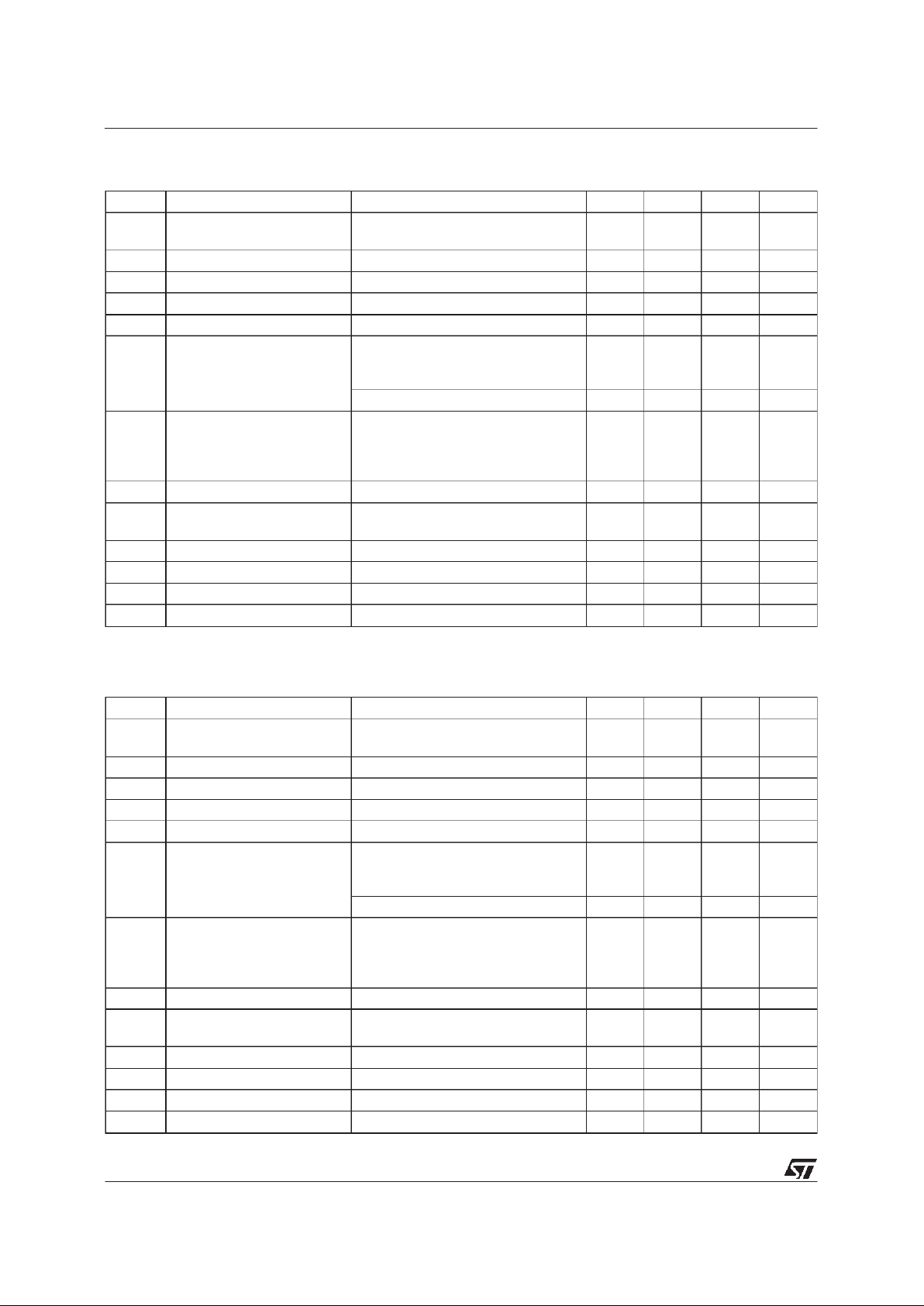
ELECTRICALCHARACTERISTICS FOR LE25AB (refer to the test circuits, Tj=25oC,
C
i
=0.1 µF, Co= 2.2 µFunlessotherwise specified)
Symbol Parameter Test Conditions Min. Typ. Max. Unit
V
o
OutputVoltage Io= 10 mA, Vi=4.5 V
I
o
= 10 mA, Vi=4.5 V -25<Ta<85oC
2.475
2.45
2.5 2. 525
2.55
V
V
V
i
OperatingInputVoltage Io= 100mA 18 V
I
out
OutputCurrent Limit 150 mA
∆V
o
LineRegulation Vi=3.2to 18 V, Io=0.5 mA 3 15 mV
∆V
o
LoadRegulation Vi=3.5V Io=0.5to 100 mA 3 15 mV
I
d
Quiescent Current ON MODE
V
i
=3.5to 18 V Io=0 mA
V
i
=3.5to 18 V Io=100 mA
0.5
1.5
1
3
mA
mA
OFF MODE V
i
= 6V 50 100 µA
SVR Supply VoltageRejection
I
o
= 5mA Vi= 4.5V ± 1V
f = 120Hz
f = 1 KHz
f = 10 KHz
82
77
60
dB
dB
dB
eN OutputNoise Voltage B = 10 Hzto 100 KHz 50 µV
V
d
DropoutVoltage Io= 100mA
I
o
= 100mA -40< Ta< 125oC
0.2 0. 4
0.5
V
V
V
il
ControlInput Logic Low -40 < Ta<125oC0.8V
V
ih
ControlInput Logic High -40 < Ta<125oC2 V
I
i
ControlInput Current Vi=6 V, Vc=6V 10 µA
C
O
OutputBypass Capacitance
ESR =0.1 to 10 Ω I
o
=0 to 100 mA
210 µF
ELECTRICALCHARACTERISTICS FOR LE25C (refer to the test circuits, Tj=25oC,
C
i
=0.1 µF, Co= 2.2 µFunlessotherwise specified)
Symbol Parameter Test Conditions Min. Typ. Max. Unit
V
o
OutputVoltage Io= 10 mA, Vi=3.3 V
I
o
= 10 mA, Vi=3.3 V -25<Ta<85oC
2.45
2.4
2.5 2.55
2.6
V
V
V
i
OperatingInputVoltage Io= 100mA 18 V
I
out
OutputCurrent Limit 150 mA
∆V
o
LineRegulation Vi=3.2to 18 V, Io=0.5 mA 3 20 mV
∆V
o
LoadRegulation Vi=3.5V Io=0.5to 100 mA 3 25 mV
I
d
Quiescent Current ON MODE
V
i
=3.5to 18 V Io=0 mA
V
i
=3.5to 18 V Io=100 mA
0.5
1.5
1
3
mA
mA
OFF MODE V
i
= 6V 50 100 µA
SVR Supply VoltageRejection
I
o
= 5mA Vi= 4.5V ± 1V
f = 120Hz
f = 1 KHz
f = 10 KHz
82
77
60
dB
dB
dB
eN OutputNoise Voltage B = 10 Hzto 100 KHz 50 µV
V
d
DropoutVoltage Io= 100mA
I
o
= 100mA -40< Ta< 125oC
0.2 0. 4
0.5
V
V
V
il
ControlInput Logic Low -40 < Ta<125oC0.8V
V
ih
ControlInput Logic High -40 < Ta<125oC2 V
I
i
ControlInput Current Vi=6 V, Vc=6V 10 µA
C
O
OutputBypass Capacitance
ESR =0.1 to 10 Ω I
o
=0 to 100 mA
210 µF
LE00AB/C
6/25
ELECTRICALCHARACTERISTICS FOR LE27AB (refer to the test circuits, Tj=25oC,
C
i
=0.1 µF, Co= 2.2 µFunlessotherwise specified)
Symbol Parameter Test Conditions Min. Typ. Max. Unit
V
o
OutputVoltage Io= 10 mA, Vi=4.7 V
I
o
= 10 mA, Vi=4.7 V -25<Ta<85oC
2.673
2.646
2.7 2. 727
2.754
V
V
V
i
OperatingInputVoltage Io= 100mA 18 V
I
out
OutputCurrent Limit 150 mA
∆V
o
LineRegulation Vi=3.4to 18 V, Io=0.5 mA 3 15 mV
∆V
o
LoadRegulation Vi=3.7V Io=0.5to 100 mA 3 15 mV
I
d
Quiescent Current ON MODE
V
i
=3.7to 18 V Io=0 mA
V
i
=3.7to 18 V Io=100 mA
0.5
1.5
1
3
mA
mA
OFF MODE V
i
= 6V 50 100 µA
SVR Supply VoltageRejection
I
o
= 5mA Vi= 4.7V ± 1V
f = 120Hz
f = 1 KHz
f = 10 KHz
82
77
60
dB
dB
dB
eN OutputNoise Voltage B = 10 Hzto 100 KHz 50 µV
V
d
DropoutVoltage Io= 100mA
I
o
= 100mA -40< Ta< 125oC
0.2 0. 4
0.5
V
V
V
il
ControlInput Logic Low -40 < Ta<125oC0.8V
V
ih
ControlInput Logic High -40 < Ta<125oC2 V
I
i
ControlInput Current Vi=6 V, Vc=6V 10 µA
C
O
OutputBypass Capacitance
ESR =0.1 to 10 Ω I
o
=0 to 100 mA
210 µF
ELECTRICALCHARACTERISTICS FOR LE27C (refer to the test circuits, Tj=25oC,
C
i
=0.1 µF, Co= 2.2 µFunlessotherwise specified)
Symbol Parameter Test Conditions Min. Typ. Max. Unit
V
o
OutputVoltage Io= 10 mA, Vi=4.7 V
I
o
= 10 mA, Vi=4.7 V -25<Ta<85oC
2.646
2.592
2.7 2. 754
2.808
V
V
V
i
OperatingInputVoltage Io= 100mA 18 V
I
out
OutputCurrent Limit 150 mA
∆V
o
LineRegulation Vi=3.4to 18 V, Io=0.5 mA 3 20 mV
∆V
o
LoadRegulation Vi=3.7V Io=0.5to 100 mA 3 25 mV
I
d
Quiescent Current ON MODE
V
i
=3.7to 18 V Io=0 mA
V
i
=3.7to 18 V Io=100 mA
0.5
1.5
1
3
mA
mA
OFF MODE V
i
= 6V 50 100 µA
SVR Supply VoltageRejection
I
o
= 5mA Vi= 4.7V ± 1V
f = 120Hz
f = 1 KHz
f = 10 KHz
82
77
60
dB
dB
dB
eN OutputNoise Voltage B = 10 Hzto 100 KHz 50 µV
V
d
DropoutVoltage Io= 100mA
I
o
= 100mA -40< Ta< 125oC
0.2 0. 4
0.5
V
V
V
il
ControlInput Logic Low -40 < Ta<125oC0.8V
V
ih
ControlInput Logic High -40 < Ta<125oC2 V
I
i
ControlInput Current Vi=6 V, Vc=6V 10 µA
C
O
OutputBypass Capacitance
ESR =0.1 to 10 Ω I
o
=0 to 100 mA
210 µF
LE00AB/C
7/25
ELECTRICALCHARACTERISTICS FOR LE30AB (refer to the test circuits, Tj=25oC,
C
i
=0.1 µF, Co= 2.2 µFunlessotherwise specified)
Symbol Parameter Test Conditions Min. Typ. Max. Unit
V
o
OutputVoltage Io= 10 mA, Vi=5 V
I
o
= 10 mA, Vi=5 V -25<Ta<85oC
2.970
2.940
3 3.030
3.060
V
V
V
i
OperatingInputVoltage Io= 100mA 18 V
I
out
OutputCurrent Limit 150 mA
∆V
o
LineRegulation Vi=3.7to 18 V, Io=0.5 mA 3 15 mV
∆V
o
LoadRegulation Vi=4V Io=0.5 to 100mA 3 15 mV
I
d
Quiescent Current ON MODE
V
i
=4to18V Io=0mA
V
i
=4to18V Io=100mA
0.5
1.5
1
3
mA
mA
OFF MODE V
i
= 6V 50 100 µA
SVR Supply VoltageRejection
I
o
= 5mA Vi=5V±1V
f = 120Hz
f = 1 KHz
f = 10 KHz
81
76
60
dB
dB
dB
eN OutputNoise Voltage B = 10 Hzto 100 KHz 50 µV
V
d
DropoutVoltage Io= 100mA
I
o
= 100mA -40< Ta< 125oC
0.2 0. 4
0.5
V
V
V
il
ControlInput Logic Low -40 < Ta<125oC0.8V
V
ih
ControlInput Logic High -40 < Ta<125oC2 V
I
i
ControlInput Current Vi=6 V, Vc=6V 10 µA
C
O
OutputBypass Capacitance
ESR =0.1 to 10 Ω I
o
=0 to 100 mA
210 µF
ELECTRICALCHARACTERISTICS FOR LE30C (refer to the test circuits, Tj=25oC,
C
i
=0.1 µF, Co= 2.2 µFunlessotherwise specified)
Symbol Parameter Test Conditions Min. Typ. Max. Unit
V
o
OutputVoltage Io= 10 mA, Vi=5 V
I
o
= 10 mA, Vi=5 V -25<Ta<85oC
2.940
2.880
3 3.060
3.120
V
V
V
i
OperatingInputVoltage Io= 100mA 18 V
I
out
OutputCurrent Limit 150 mA
∆V
o
LineRegulation Vi=3.7to 18 V, Io=0.5 mA 3 20 mV
∆V
o
LoadRegulation Vi=4V Io=0.5 to 100mA 3 25 mV
I
d
Quiescent Current ON MODE
V
i
=4to18V Io=0mA
V
i
=4to18V Io=100mA
0.5
1.5
1
3
mA
mA
OFF MODE V
i
= 6V 50 100 µA
SVR Supply VoltageRejection
I
o
= 5mA Vi=5V±1V
f = 120Hz
f = 1 KHz
f = 10 KHz
81
76
60
dB
dB
dB
eN OutputNoise Voltage B = 10 Hzto 100 KHz 50 µV
V
d
DropoutVoltage Io= 100mA
I
o
= 100mA -40< Ta< 125oC
0.2 0. 4
0.5
V
V
V
il
ControlInput Logic Low -40 < Ta<125oC0.8V
V
ih
ControlInput Logic High -40 < Ta<125oC2 V
I
i
ControlInput Current Vi=6 V, Vc=6V 10 µA
C
O
OutputBypass Capacitance
ESR =0.1 to 10 Ω I
o
=0 to 100 mA
210 µF
LE00AB/C
8/25
 Loading...