

SGS Thomson Microelectronics LDO-57 Datasheet
1/4June 2002
IP Library: High Out put Current, Low power,
400mA Low Dropout Voltage Regu lator
■
DIGITAL BASEBAND REGULATOR
■
VERY LOW DROPOUT VOLTAGE : 50mV
■
HIGH OUTPUT CURRENT : 400mA
■
LOW QUIESCENT CURRENT : 100µA
■
HIGH PSRR : 60dB
■
LOW OU TPU T VOLTAGE NOI SE
■
NO CURRENT IN POWER DOWN MODE
■
SHORT CIRCUIT PROTECTION
TYPICAL APPLICATIONS
– Cellular and Cordless phones suppli ed by 1 cell
Lithium-ion battery / 3 cells Ni-MH or Ni-Cd
battery.
– PDA (Personal Digital Assistant), Smart phone.
– Portable equipm ent.
– Supply for Digital Baseband devices for cellular
phone.
APPLICATION NOTE
An external capacitor (C
OUT
= 4.7µF) with an
equivalent serial resistance (ESR) in the range
0.02 to 0.6Ω is used for regulator stability.
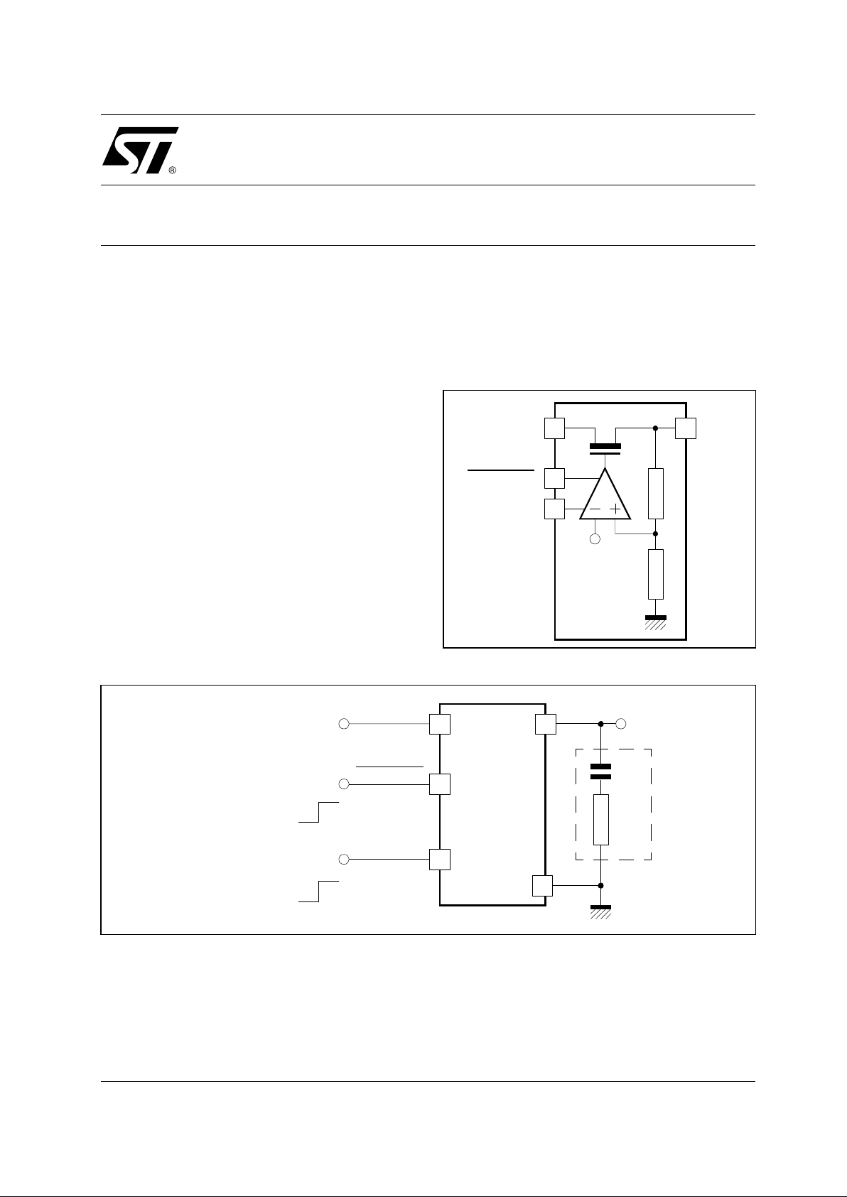
Figure 1 :
Block Diagram
?
V
REF
?
?
?
LDO_57
OUTIN
PWRDWN
STDBY
Figure 2 :
Typical Application Circuit
4.7µF
ESR
V
OUT
C
OUT
?
?
OUT
GND
?
?
?
V
IN
IN
PWRDWN
Power Down Mode
OFF
ON
Stand-by Mode
STDBY
Active Mode
LDO_57
→
→
Stand-by Mode
→
→
LDO_57
This is advance information on a new product now in development or undergoing evaluation. Details are subject to change without notice.
PRODUCT PREVIEW
LDO_57
2/4
ELECTRICAL CHARACTERISTICS
3V < V
IN
< 5.5V, -30°C < TA < +85°C, V
REF
= 2.8V, C
OUT
= 4.7µF ±20%, 20mΩ < ESR < 0.6Ω,
I
LOAD
= 400mA.
Typical case :
V
IN
= 4V, T = 25°C, C
OUT
= 4.7µF, I
LOAD
= 400mA.
Notes: 1. Above characteristics are given for 2.9V minimum input operating range voltage, but regulator
is operational with 2.7V minimum input voltage.
2. All performances of the regulator are guarenteed for a voltage drop of 170mV minimum.
Parameter Symbol Test Condition Min Typ Max Unit
Input Voltage Range (Note 1) V
IN
2,9 5,5 V
Output Voltage V
OUT
1,8 4,9 V
Output Voltage Accuracy 3 %
Output current I
OUT
400 mA
Dropout Voltage ∆V
DO
∆V
OUT
= 50mV,
I
LOAD
= 400mA,
50 mV
(Note 2) 170 mV
Quiescent current I
Q
I
LOAD
= 100µA 100 150 µA
I
LOAD
= 40mA 150 230
I
LOAD
= 400mA 350 450
Power down mode quiescent current I
QPDM
Power down active 100 nA
Power Supply Rejection Ratio PSRR DC 40 60 dB
f = 10KHz 40 55
Line Regulation Lir I
LOAD
= 400mA,
VIN = 2.9V to 5.5V
4mV
Load Regulation Ldr I
LOAD
= 100µA - 400mA 50 55 mV
Line Transient Lirt ∆V
IN
= 300mV
t
RISE
= t
FALL
= 10µs
2,5 5 mV
Load Transient Ldtr I
LOAD
= 100µA - 400mA
in 10µs
35mV
Output Noise Voltage en 100Hz 1,2
1KHz 400
10KHz 140
en
RMS
BW : 100Hz to 100KHz 35 µV
RMS
Output decoupling Capacitor C
OUT
4,7 µF
Settling time From power down
to active mode
50 µs
Short Circuit Current Limit I
SHORT
2A
µV
Hz
----------- -
nV
Hz
----------- -
 Loading...