

1/4June 2002
■
CHARGE CONTROL REGULATOR
■
VERY LOW DROPOUT VOLTAGE : 60mV
■
LARGE INPUT VOLTAGE RAN GE
■
OUTPUT CURRENT : 50mA
■
LOW QUIESCENT CURRENT : 280µA
■
HIGH PSRR : 6 0dB
■
NO CURRENT IN POWER DOWN MODE
■
SHORT CIRCUIT PROTECTION
TYPICAL APPLICATIONS
– Cellular and Cordless phones suppli ed by 1 cell
Lithium-ion battery / 3 cells Ni-MH or Ni-Cd
battery
– PDA (Personal Digital Assistant), Smart phone
– Portable equipm ent
– Supply for Charge control devices of cellular
phone
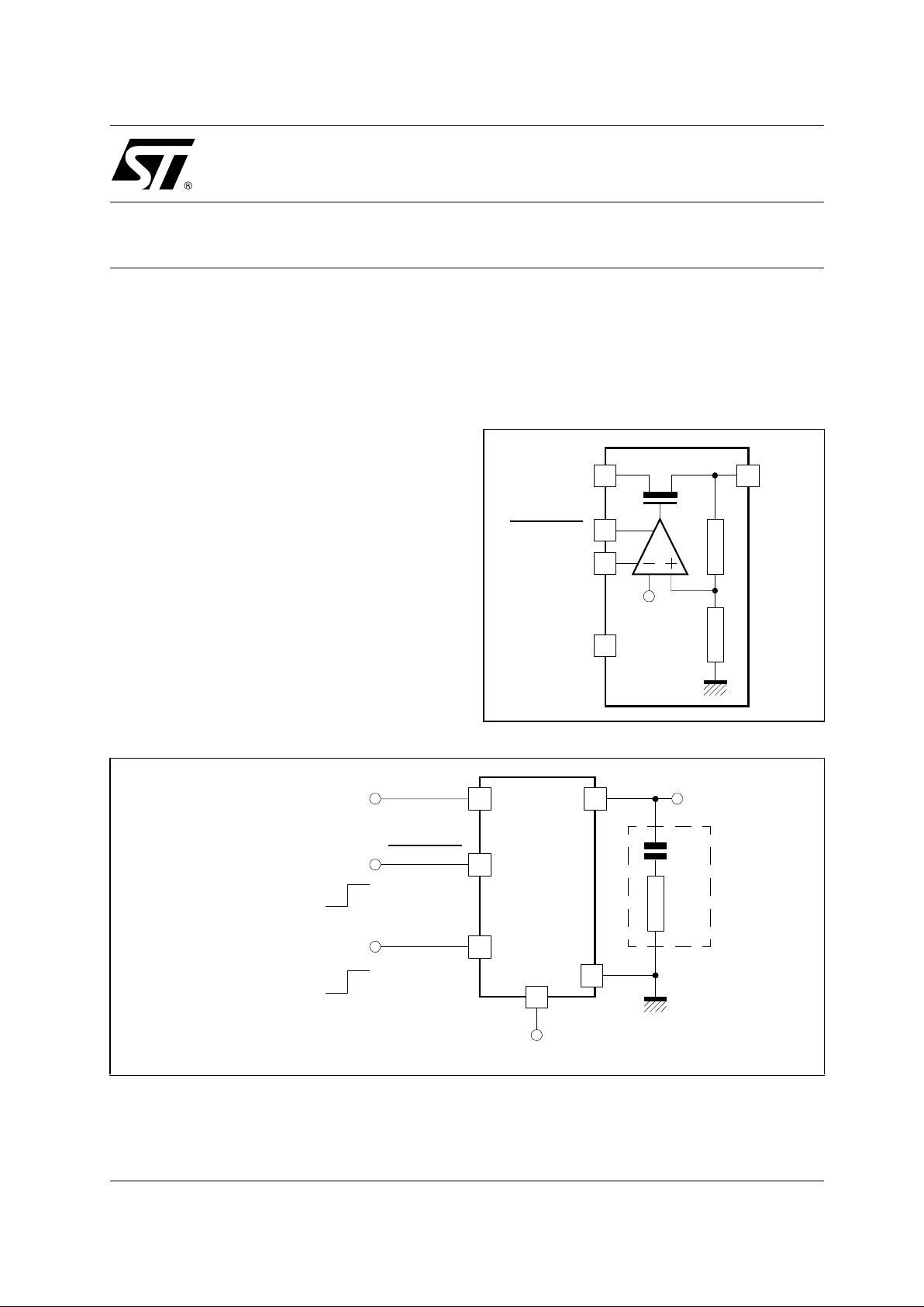
APPLICATION NOTE
An external capacitor (C
OUT
= 1µF) with an
equivalent serial resistance (ESR) in the range
0.02 to 0.6Ω is used for regulator stability.
The regulator needs two separated power
supplies, one (V
5V
) for the digital parts and
programming inputs (Stand-by and Power-down
mode) which cannot exceed 5V and one (Vin) as
the input voltage of the regulator.
Figure 1 :
Block Diagram
?
V
REF
?
?
?
LDO_513
OUTIN
PWRDWN
STDBY
?
V
5V
Figure 2 :
Typical Application Circuit
1µF
ESR
V
OUT
C
OUT
?
?
OUT
GND
?
?
?
V
IN
IN
PWRDWN
Power Down Mode
OFF
ON
Stand-by Mode
STDBY
Active Mode
LDO_513
→
→
Stand-by Mode
→
→
?
5V Power Supply
V
5V
LDO_513
This is advance informati on on a new product now in development or undergoing evaluation. Details are subject to change w ithout notice.
PRODUCT PREVIEW
IP Library: Powe r Supply Range 2.9V to 13V, Low Power,
50mA Low Dropout Volt age Regulator
LDO_513
2/4
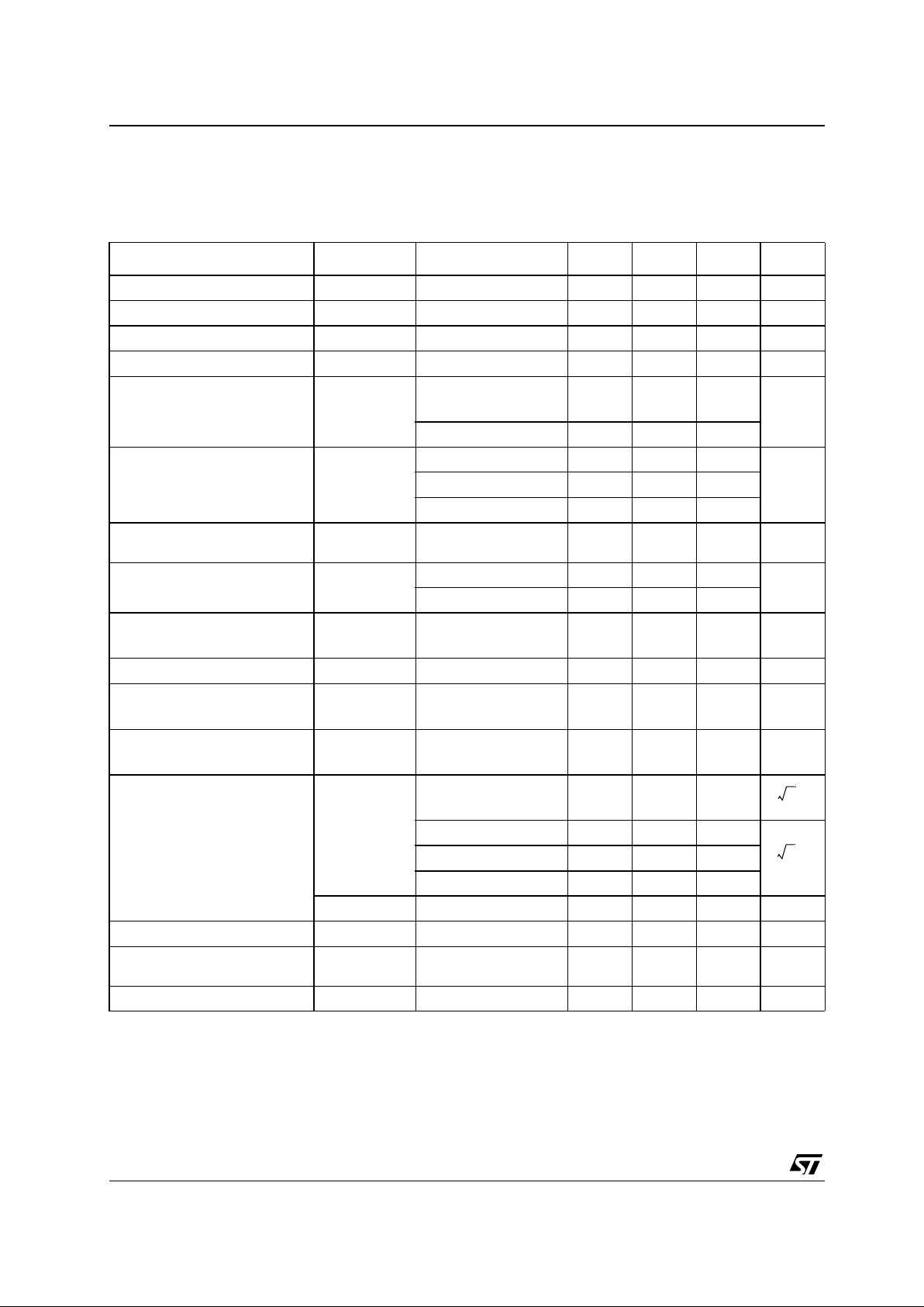
ELECTRICAL CHARACTERISTI CS
2.9V < V
IN
< 13V, -30°C < TA < +85°C, C
OUT
= 1µF ±20%, 20mΩ < ESR < 0. 6Ω, I
LOAD
= 50mA.
Typical case: V
IN
= 4V, T = 25°C, C
OUT
= 1µF.
Notes: 1. Above characteristics are given for 2.9V minimum input operating range voltage, but regulator
is operational with 2.7V minimum input voltage.
2. All parameters are guaranteed with 200mV min Dropout voltage.
Parameter Symbol Test Condition Min. Typ. Max. Unit
Input Voltage Range (Note 1) V
IN
2.9 13 V
Output Voltage Vout 1.8 5 V
Output Voltage Accuracy 3 %
Output current I
OUT
50 mA
Dropout Voltage ∆V
DO
∆V
OUT
= 50mV,
I
LOAD
= 50mA
70 mV
(Note 2) 200
Quiescent current I
Q
I
LOAD
= 100µA 40 µA
I
LOAD
= 10mA 100
I
LOAD
= 50mA 270 340
Power down mode quiescent
current
I
QPDM
Power down active 100 nA
Power Supply Rejection Ratio PSRR DC 45 60 dB
f = 10KHz 40 60
Line Regulation L
IR
I
LOAD
= 50mA,
V
IN
= 3V to 13V
3mV
Load Regulation L
DR
I
LOAD
= 100µA - 50mA 40 mV
Line Transient L
IRT
∆V
IN
= 300mV
t
RISE
= t
FALL
= 10µs
3mV
Load Transient L
DTR
I
LOAD
=100µA - 50mA
in 10µs
6mV
Output Noise Voltage en 100Hz 1.2
1KHz 400
10KHz 150
100KHz 70
en
RMS
BW : 100Hz to 100KHz 35 µV
RMS
Output decoupling Capacitor C
OUT
1µF
Settling time From power down to
active mode
120 µs
Short Circuit Current Limit I
SHORT
100 220 mA
µV
Hz
----------- -
nV
Hz
----------- -
 Loading...