

SGS Thomson Microelectronics LD2979Z50, LD2979Z38, LD2979Z33, LD2979Z32, LD2979Z30 Datasheet
...
LD2979
VOLTAGE REGULATORS WITH INHIBIT
■ VERYLOWDROPOUTVOLTAGE
(0.2VTYP.AT50mALOAD)
■ VERYLOWQUIESCENTCURRENT
(TYP.500µA AT50mALOAD)
■ OUTPUT CURRENT UP TO50 mA
■ LOGIC-CONTROLLEDELECTRONIC
SHUTDOWN
■ OUTPUT VOLTAGESOF 2.85;3.0;3.2;3.3;
3.8;5.0V
■ INTERNALCURRENT AND THERMAL LIMIT
■ SUPPLYVOLTAGEREJECTION:63dB(TYP)
■ ONLY1µF FORSTABILITY
■ SELECTIONAT 25
■ TEMPERATURERANGE:-25 TO 125
■ PACKAGEAVAILABLE:SOT23-5LANDTO-92
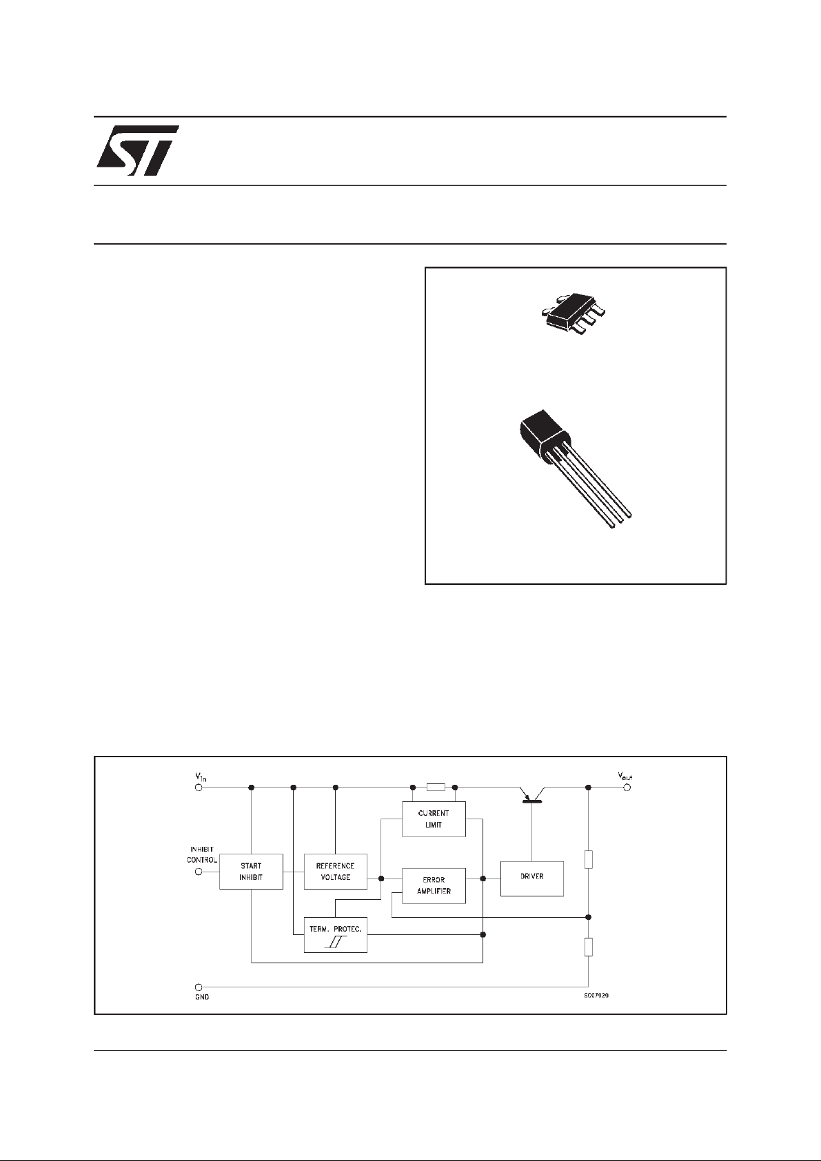
DESCRIPTION
The LD2979 series are very Low Drop regulators
availablein SOT23-5Land TO-92.
The very low drop-voltage and the very low
quiescent current make them particularlysuitable
for low noise, low power applications and in
batterypowered systems.
Shutdown Logic Control function is available on
five pin version (TTL compatible). This means
o
C
o
C
SERIES
VERY LOW DROP
SOT23-5L
TO-92
that when the device is used as local regulator, it
is possible to put a part of the board in standby,
decreasingthe total powerconsumption.
SCHEMATIC DIAGRAM
April 2000
1/9
LD2979
ABSOLUTE MAXIMUM RATING
Symbol Parameter Value Unit
DC InputVoltage 16 V
V
IN
V
DC Inhibit InputVoltage V
INH
OutputCurrent Internally limited mA
I
o
PowerDissipation Internally limited mW
P
tot
StorageTemperature Range - 40 to 150
T
stg
OperatingJunctionTemperatureRange - 25 to 125
T
op
IN
V
o
C
o
C
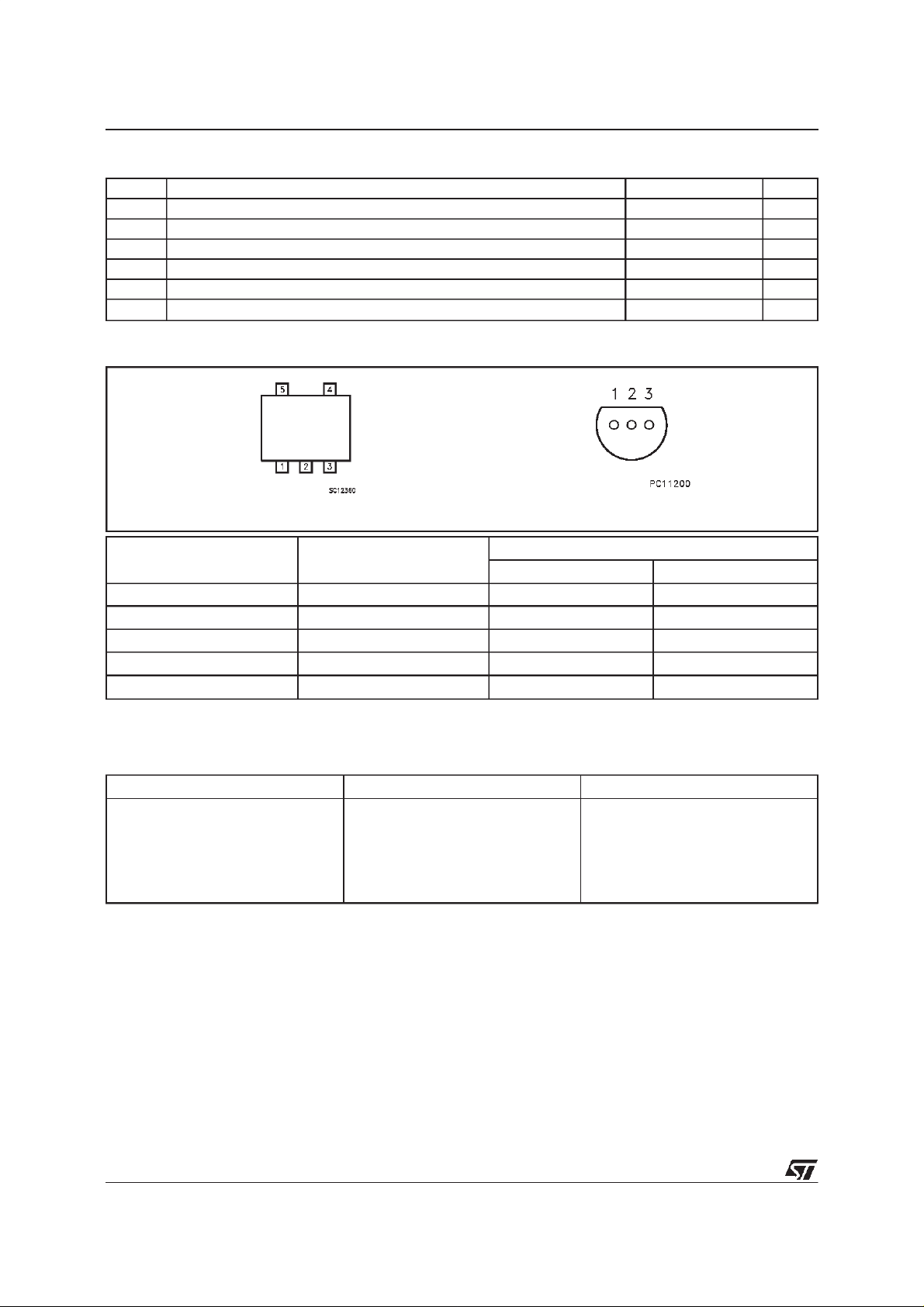
CONNECTION DIAGRAM
(topview)
BOTTOM
VIEW
SOT23-5L TO-92
SYMBOL NAME AND FUNCTION PIN NUMBER
SOT23-5L TO-92
V
IN
Input V o lt age 1 3
GND Gr ound 2 2
INHIBIT Control Switch ON/OFF (*) 3 -
NC Not to be conne c t ed 4 -
V
OUT
(*) Only for the version in SOT23-5L package: Inhibitpin is not internally pulled-up then it must not be left floating. Connect toa positive
voltage higher than 2V to able the device.
Out put Voltage 5 1
ORDERING NUMBERS
SOT23-5L TO-92 OutputVoltage
LD2979M28
LD2979M30
LD2979M32
LD2979M33
LD2979M38
LD2979M50
LD2979Z28
LD2979Z30
LD2979Z32
LD2979Z33
LD2979Z38
LD2979Z50
2.85 V
3.0 V
3.2 V
3.3 V
3.8 V
5.0 V
2/9
LD2979
ELECTRICALCHARACTERISTICS FOR LD2979 (refer to the test circuits, Ta=25oC,
V
IN=VO(NOM)
+1, CO=1µF, IO= 1mA, V
inh
(*)
=2V
) (unlessotherwise specified)
Symbol Parameter Test Conditions Min. Typ. Max. Unit
OutputVoltage VIN=3.85 V
V
o
OutputVoltage VIN=4V
V
o
OutputVoltage VIN=4.2 V
V
o
OutputVoltage VIN=4.3 V
V
o
OutputVoltage VIN=4.8 V
V
o
OutputVoltage VIN=6V
V
o
OutputCurrentLimit 100 mA
I
out
LineRegulation V
V
∆
o
I
QuiescentCurrent ON MODE
d
<50 mA, -25< Ta< 125oC
1<I
o
<50 mA, -25< Ta< 125oC
1<I
o
<50 mA, -25< Ta< 125oC
1<I
o
<50 mA, -25< Ta< 125oC
1<I
o
<50 mA, -25< Ta< 125oC
1<I
o
<50 mA, -25< Ta< 125oC
1<I
o
+1< VIN<16V, Io=1mA
O(NOM)
-25 < T
I
I
I
I
<125oC
a
=0mA
o
=0 mA -25< Ta<125oC
o
=50mA
o
=50 mA -25< Ta< 125oC
o
2.793
2.736
2.940
2.880
3.136
3.072
3.234
3.168
3.724
3.648
4.9
4.8
2.85 2.907
2.964
33.060
3.120
3.2 3. 264
3.328
3.3 3. 366
3.432
3.8 3. 876
3.952
55.1
5.2
0.028
0.064
80
110
170
500
700
1300
%/V
OFF MODE(*)
< 0.18 V
V
ihn
< 0.18 V -25< Ta<125oC
V
ihn
SVR Supply Voltage Rejection I
Dropout Voltage Io=0mA
V
d
Control InputLogicLow -25 < Ta<125oC(*) DeviceOff 0.18 V
V
il
Control InputLogicHigh -25 < Ta<125oC(*) DeviceOn 2 V
V
ih
Control InputCurrent V
I
i
=50 mA, f= 120Hz, C
o
=0 mA -25< Ta<125oC
I
o
=1mA
I
o
=1 mA -25< Ta<125oC
I
o
=10mA
I
o
=10 mA -25< Ta< 125oC
I
o
=50mA
I
o
=50 mA -25< Ta< 125oC
I
o
=0 V (*)
inhibit
=5 V, -25< Ta<125oC (*)
V
inhibit
eN OutputNoise Voltage(RMS) BW = 300Hz to50 KHz, C
(*) Note: Only for types inSOT23-5L
=10µF63 dB
out
=10µF160
out
0
6
30
100
200
0
5
1
12
18
60
90
200
300
400
600
-1
15
V
V
V
V
V
V
V
V
V
V
V
V
in
A
µ
A
µ
A
µ
A
µ
µA
A
µ
mV
mV
mV
mV
mV
mV
mV
mV
A
µ
A
µ
V
µ
3/9
 Loading...