

Datasheet LD1117VC, LD1117V50C, LD1117V50, LD1117V33, LD1117F12 Datasheet (SGS Thomson Microelectronics)
...
1/24October 2003
■ LOW DROPOUT VOLTAGE (1V TYP.)
■ 2.85V DEVICE PERFORMANCES ARE
SUITABLE FOR SCSI-2 ACTIVE
TERMINATION
■ OUTPUT CURRENT UP TO 800 mA
■ FIXED OUTPUT VOLTAGE OF: 1.2V, 1.8V,
2.5V, 2 .85V, 3.0V, 3.3V, 5.0V
■ ADJUSTABLE VERSION AVAILABILITY
(V
rel
=1.25V)
■ INTERNAL CURRENT AND THERMAL LIMIT
■ AVAILABLEIN ± 1% (AT 25°C) AND 2% IN
FULL TEMPERATURE RANGE
■ SUPPLY VOLTAGE REJECTION: 75dB (TYP.)
DESCRIPTION
The LD1117 is a LOW DROP Voltage Regulator
able to provide up to 800m A of Output Current,
available even in adjustable version (V re f= 1.25V).
Concerning fixed v ers ions, are offered t he
following Output Voltages: 1.2V,1.8V,2.5V,2.85V,
3.0V 3.3V and 5.0V. The 2.85V type is ideal for
SCSI-2 lines active termination. The device is
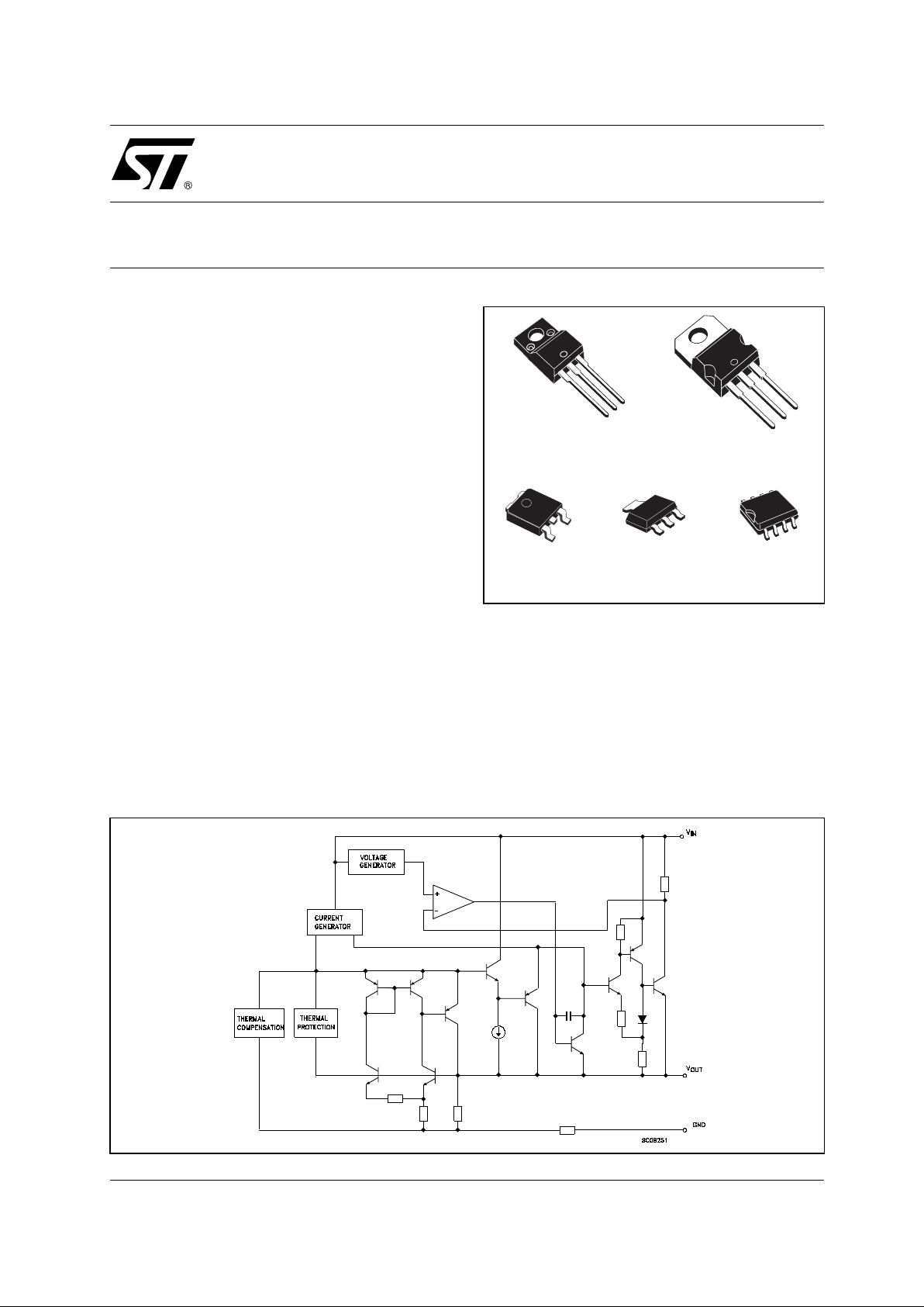
supplied in: SOT-223, DPAK, SO-8, TO -220 and
TO-220FM. The SOT-223 and DPAK surface
mount packages optimize the thermal
characteristics even offering a relevant space
saving effect. High efficiency is assured by NPN
pass transistor. In fact in this case, unlike than
PNP one, the Quiescent Current flows mostly into
the load. Only a very commo n 10µF minim um
capacitor is ne eded for stability. On chip trimming
allows the regulator to reach a very tight out put
voltage tolerance, within ± 1% at 25°C. The
ADJUSTABLE LD1117 is pin to pin compatible
with the other standard. Adjustable voltage
regulators maintainin g the better performances in
terms of D rop and Tolerance.
LD1117
SERIES
LOW DROP F IXED AND ADJUSTABLE
POSITIVE VOLTAGE REGULATORS
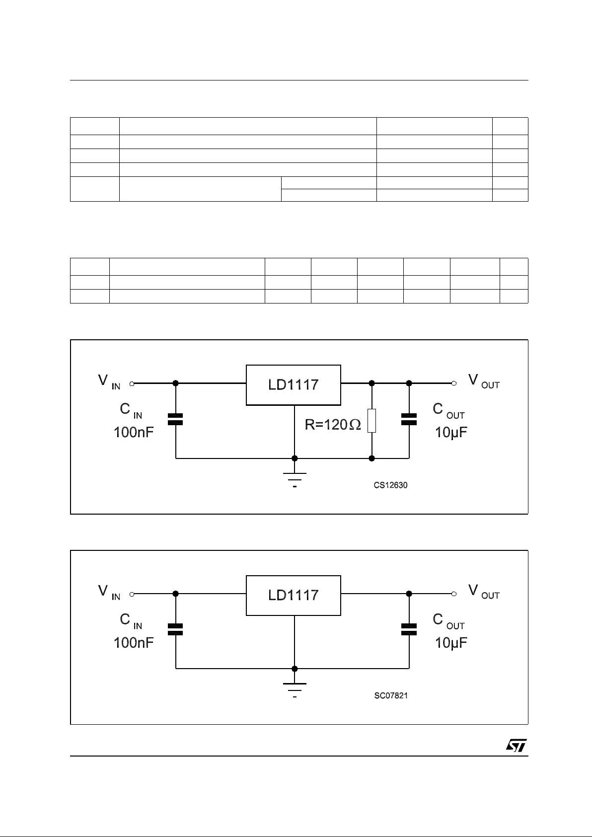
BLOCK DIAGRAM
SOT-223DPAK
TO-220FM
SO-8
TO-220
LD1117 SERIES
2/24
ABSOLUTE MAXIMUM RAT INGS
Absolute Maximum Ratings are those values beyond which damage to the device may occur. Functional operation under these condition is
not implied. Over the above suggested Max Power Dissipation a Short Circuit could definitively damage the device.
THERMAL DATA
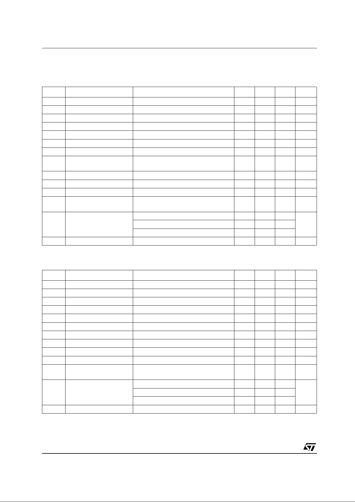
APPLICATION CIRCUIT (FOR 1.2 V)
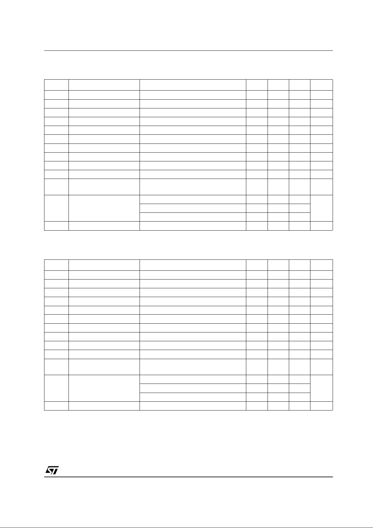
APPLICATION CIRCUIT (FOR OTHER FIXED OUTPUT VOLTAGES)
Symbol Parameter² Value Unit
V
IN
DC Input Voltage
15 V
P
tot
Power Dissipation
12 W
T
stg
Storage Temperature Range
-40 to +150 °C
T
op
Operating Junction Temperature Range for C Version -40 to +125 °C
for standard Version 0 to +125 °C
Symbol Parameter SOT-223 SO-8 DPAK TO-220 TO-220FM Unit
R
thj-case
Thermal Resistance Junction-case
15 20 8 3 4 °C/W
R
thj-amb
Thermal Resistance Junction-ambient
50 60 °C/W

LD1117 SERIES
3/24
CONNECTION DIAGRAM (top v iew)
NOTE: The TAB is connected to the V
OUT
.
ORDERING CODES
SOT-223 SO-8 DPAK TO-220 TO-220FM
OUTPUT
VOLTAGE
LD1117S12 LD1117D12 (*) LD1117DT12 LD1117V12 (*) LD1117F12 (*) 1.2 V
LD1117S18 LD1117D18 LD1117DT18 LD1117V18 LD1117F18 1.8 V
LD1117S18C LD1117D18C LD1117DT18C LD1117V18C LD1117F18C 1.8 V
LD1117S25 LD1117D25 LD1117DT25 LD1117V25 LD1117F25 2.5 V
LD1117S25C LD1117D25C LD1117DT25C LD1117V25C LD1117F25C 2.5 V
LD1117S28 LD1117D28 LD1117DT28 LD1117V28 LD1117F28 2.85 V
LD1117S30 LD1117D30 LD1117DT30 LD1117V30 LD1117F30 3 V
LD1117S30C LD1117D30C LD1117DT30C LD1117V30C LD1117F30C 3 V
LD1117S33 LD1117D33 LD1117DT33 LD1117V33 LD1117F33 3.3 V
LD1117S33C LD1117D33C LD1117DT33C LD1117V33C LD1117F33C 3.3 V
LD1117S50 LD1117D50 LD1117DT50 LD1117V50 LD1117F50 5 V
LD1117S50C LD1117D50C LD1117DT50C LD1117V50C LD1117F50C 5 V
LD1117S LD1117D LD1117DT LD1117V LD1117F ADJUSTABLE
FROM 1.25 TO
15V
LD1117SC LD1117DC LD1117DTC LD1117VC LD1117FC ADJUSTABLE
FROM 1.25 TO
15V
SOT-223 SO-8
TO-220FM
DPAK
TO-220
LD1117 SERIES
4/24
(*) Available on request
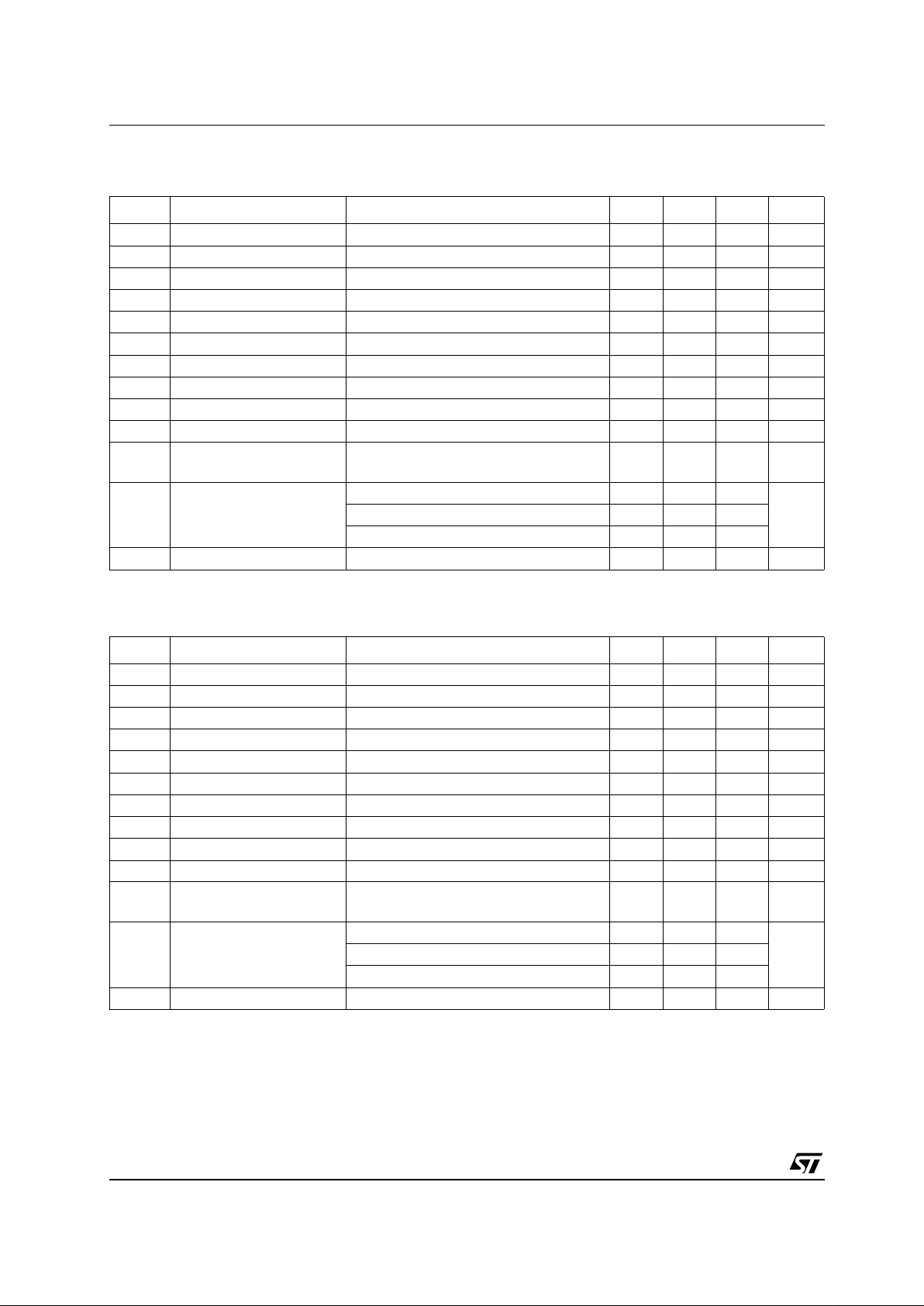
ELECTRICAL CHARACTERISTICS OF LD1117#12 (refer to the test circuits, TJ= 0 to 125° C,
C
O
= 10 µF, R = 120 Ω b etwe en GND and OUT pi ns , unless otherwise specified)
ELECTRICAL CHARACTERISTICS OF LD1117#18 (refer to the test circuits, T
J
= 0 to 125° C,
C
O
= 10 µF unless otherwise specified)
Symbol Parameter Test Conditions Min. Typ. Max. Unit
V
ref
Reference Voltage IO=10to800mA Vin-VO= 1.4 to 10 V 1.140 1.20 1.260 V
∆V
O
Line Regulation Vin-VO= 1.5 to 13.75 V IO= 10 mA 0.035 0.2 %
∆V
O
Load Regulation Vin-VO=3V IO= 10 to 800 mA 0.1 0.4 %
∆V
O
Temperature Stability 0.5 %
∆V
O
Long Term Stability 1000 hrs, TJ= 125°C 0.3 %
V
in
Operating Input Voltage 15 V
I
adj
Adjustment Pin Current Vin≤ 15 V 60 120 µA
∆I
adj
Adjustment Pin Current
Change
Vin-VO= 1.4 to 10 V
I
O
=10to800mA
15µA
I
O(min)
Minimum Load Current Vin=15V 2 5 mA
I
O
Output Current Vin-VO=5V TJ= 25°C 800 950 1300 mA
eN Output Noise (%V
O
) B =10Hz to 10KHz TJ= 25°C 0.003 %
SVR Supply Voltage Rejection I
O
= 40 mA f = 120Hz TJ= 25°C
V
in-VO
=3V V
ripple
=1V
PP
60 75 dB
V
d
Dropout Voltage IO= 100 mA 1 1.1 V
I
O
= 500 mA 1.05 1.15
I
O
= 800 mA 1.10 1.2
Thermal Regulation T
a
= 25°C 30ms Pulse 0.01 0.1 %/W
Symbol Parameter Test Conditions Min. Typ. Max. Unit
V
O
Output Voltage Vin= 3.8 V IO=10mA TJ= 25°C 1.78 1.8 1.82 V
V
O
Output Voltage IO= 0 to 800 mA Vin= 3.3 to 8 V 1.76 1.84 V
∆V
O
Line Regulation Vin= 3.3 to 8 V IO= 0 mA 1 6 mV
∆V
O
Load Regulation Vin= 3.3 V IO= 0 to 800 mA 1 10 mV
∆V
O
Temperature Stability 0.5 %
∆V
O
Long Term Stability 1000 hrs, TJ= 125°C 0.3 %
V
in
Operating Input Voltage IO= 100 mA 10 V
I
d
Quiescent Current Vin≤ 8V 5 10 mA
I
O
Output Current Vin= 6.8 V TJ= 25°C 800 950 1300 mA
eN Output Noise Voltage B =10Hz to 10KHz T
J
= 25°C 100 µV
SVR Supply Voltage Rejection I
O
= 40 mA f = 120Hz TJ= 25°C
V
in
= 5.5 V V
ripple
=1V
PP
60 75 dB
V
d
Dropout Voltage IO= 100 mA 1 1.1 V
I
O
= 500 mA 1.05 1.15
I
O
= 800 mA 1.10 1.2
Thermal Regulation T
a
= 25°C 30ms Pulse 0.01 0.1 %/W
LD1117 SERIES
5/24
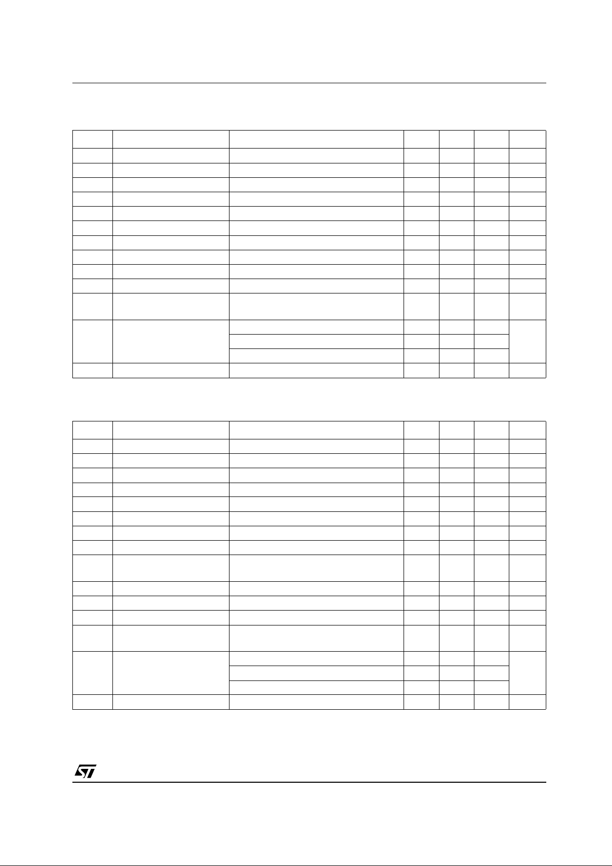
ELECTRICAL CHARACTERISTICS OF LD1117#25 (refer to the test circuits, TJ= 0 to 125° C,
C
O
= 10 µF unless otherwise specified)
ELECTRICAL CHARACTERISTICS OF LD1117#28 (refer to the test circuits, T
J
= 0 to 125° C,
C
O
= 10 µF unless otherwise specified)
Symbol Parameter Test Conditions Min. Typ. Max. Unit
V
O
Output Voltage Vin= 4.5 V IO=10mA TJ= 25°C 2.475 2.5 2.525 V
V
O
Output Voltage IO= 0 to 800 mA Vin= 3.9 to 10 V 2.45 2.55 V
∆V
O
Line Regulation Vin= 3.9 to 10 V IO= 0 mA 1 6 mV
∆V
O
Load Regulation Vin= 3.9 V IO= 0 to 800 mA 1 10 mV
∆V
O
Temperature Stability 0.5 %
∆V
O
Long Term Stability 1000 hrs, TJ= 125°C 0.3 %
V
in
Operating Input Voltage IO= 100 mA 15 V
I
d
Quiescent Current Vin≤ 10 V 5 10 mA
I
O
Output Current Vin= 7.5 V TJ= 25°C 800 950 1300 mA
eN Output Noise Voltage B =10Hz to 10KHz T
J
= 25°C 100 µV
SVR Supply Voltage Rejection I
O
= 40 mA f = 120Hz TJ= 25°C
V
in
= 5.5 V V
ripple
=1V
PP
60 75 dB
V
d
Dropout Voltage IO= 100 mA 1 1.1 V
I
O
= 500 mA 1.05 1.15
I
O
= 800 mA 1.10 1.2
Thermal Regulation T
a
= 25°C 30ms Pulse 0.01 0.1 %/W
Symbol Parameter Test Conditions Min. Typ. Max. Unit
V
O
Output Voltage Vin= 4.85 V IO=10mA TJ= 25°C 2.82 2.85 2.88 V
V
O
Output Voltage IO= 0 to 800 mA Vin= 4.25 to 10 V 2.79 2.91 V
∆V
O
Line Regulation Vin= 4.25 to 10 V IO= 0 mA 1 6 mV
∆V
O
Load Regulation Vin= 4.25 V IO= 0 to 800 mA 1 10 mV
∆V
O
Temperature Stability 0.5 %
∆V
O
Long Term Stability 1000 hrs, TJ= 125°C 0.3 %
V
in
Operating Input Voltage IO= 100 mA 15 V
I
d
Quiescent Current Vin≤ 10 V 5 10 mA
I
O
Output Current Vin= 7.85 V TJ= 25°C 800 950 1300 mA
eN Output Noise Voltage B =10Hz to 10KHz T
J
= 25°C 100 µV
SVR Supply Voltage Rejection I
O
= 40 mA f = 120Hz TJ= 25°C
V
in
= 5.85 V V
ripple
=1V
PP
60 75 dB
V
d
Dropout Voltage IO= 100 mA 1 1.1 V
I
O
= 500 mA 1.05 1.15
I
O
= 800 mA 1.10 1.2
Thermal Regulation T
a
= 25°C 30ms Pulse 0.01 0.1 %/W
LD1117 SERIES
6/24
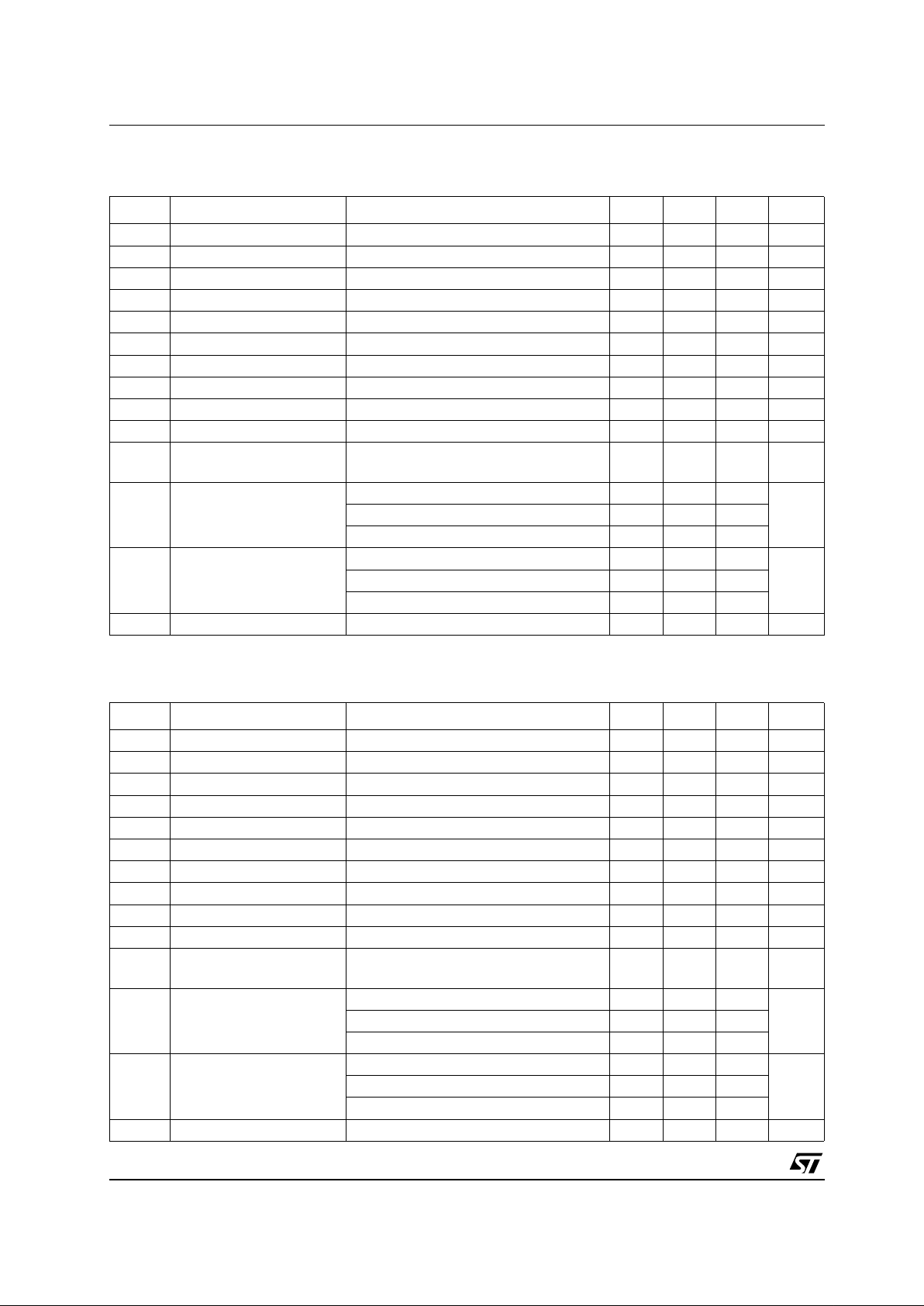
ELECTRICAL CHARACTERISTICS OF LD1117#30 (refer to the test circuits, TJ= 0 to 125° C,
C
O
= 10 µF unless otherwise specified)
ELECTRICAL CHARACTERISTICS OF LD1117#33 (refer to the test circuits, T
J
= 0 to 125° C,
C
O
= 10 µF unless otherwise specified)
Symbol Parameter Test Conditions Min. Typ. Max. Unit
V
O
Output Voltage Vin=5V IO=10mA TJ= 25°C 2.97 3 3.03 V
V
O
Output Voltage IO= 0 to 800 mA Vin= 4.5 to 10 V 2.94 3.06 V
∆V
O
Line Regulation Vin= 4.5 to 12 V IO= 0 mA 1 6 mV
∆V
O
Load Regulation Vin= 4.5 V IO= 0 to 800 mA 1 10 mV
∆V
O
Temperature Stability 0.5 %
∆V
O
Long Term Stability 1000 hrs, TJ= 125°C 0.3 %
V
in
Operating Input Voltage IO= 100 mA 15 V
I
d
Quiescent Current Vin≤ 12 V 5 10 mA
I
O
Output Current Vin=8V TJ= 25°C 800 950 1300 mA
eN Output Noise Voltage B =10Hz to 10KHz T
J
= 25°C 100 µV
SVR Supply Voltage Rejection I
O
= 40 mA f = 120Hz TJ= 25°C
V
in
=6V V
ripple
=1V
PP
60 75 dB
V
d
Dropout Voltage IO= 100 mA 1 1.1 V
I
O
= 500 mA 1.05 1.15
I
O
= 800 mA 1.10 1.2
Thermal Regulation T
a
= 25°C 30ms Pulse 0.01 0.1 %/W
Symbol Parameter Test Conditions Min. Typ. Max. Unit
V
O
Output Voltage Vin= 5.3 V IO=10mA TJ= 25°C 3.267 3.3 3.333 V
V
O
Output Voltage IO= 0 to 800 mA Vin= 4.75 to 10 V 3.235 3.365 V
∆V
O
Line Regulation Vin= 4.75 to 15 V IO= 0 mA 1 6 mV
∆V
O
Load Regulation Vin= 4.75 V IO= 0 to 800 mA 1 10 mV
∆V
O
Temperature Stability 0.5 %
∆V
O
Long Term Stability 1000 hrs, TJ= 125°C 0.3 %
V
in
Operating Input Voltage IO= 100 mA 15 V
I
d
Quiescent Current Vin≤ 15 V 5 10 mA
I
O
Output Current Vin= 8.3 V TJ= 25°C 800 950 1300 mA
eN Output Noise Voltage B =10Hz to 10KHz T
J
= 25°C 100 µV
SVR Supply Voltage Rejection I
O
= 40 mA f = 120Hz TJ= 25°C
V
in
= 6.3 V V
ripple
=1V
PP
60 75 dB
V
d
Dropout Voltage IO= 100 mA 1 1.1 V
I
O
= 500 mA 1.05 1.15
I
O
= 800 mA 1.10 1.2
Thermal Regulation T
a
= 25°C 30ms Pulse 0.01 0.1 %/W
LD1117 SERIES
7/24
ELECTRICAL CHARACTERISTICS OF LD1117#50 (refer to the test circuits, TJ= 0 to 125° C,
C
O
= 10 µF unless otherwise specified)
ELECTRICAL CHARACTERISTICS OF LD1117 (ADJ USTABLE) (refer to the tes t circuits,
T
J
= 0 to 125° C, CO= 10 µF unless otherwise specified)
Symbol Parameter Test Conditions Min. Typ. Max. Unit
V
O
Output Voltage Vin=7V IO=10mA TJ= 25°C 4.95 5 5.05 V
V
O
Output Voltage IO= 0 to 800 mA Vin= 6.5 to 15 V 4.9 5.1 V
∆V
O
Line Regulation Vin= 6.5 to 15 V IO= 0 mA 1 10 mV
∆V
O
Load Regulation Vin= 6.5 V IO= 0 to 800 mA 1 15 mV
∆V
O
Temperature Stability 0.5 %
∆V
O
Long Term Stability 1000 hrs, TJ= 125°C 0.3 %
V
in
Operating Input Voltage IO= 100 mA 15 V
I
d
Quiescent Current Vin≤ 15 V 5 10 mA
I
O
Output Current Vin=10V TJ= 25°C 800 950 1300 mA
eN Output Noise Voltage B =10Hz to 10KHz T
J
= 25°C 100 µV
SVR Supply Voltage Rejection I
O
= 40 mA f = 120Hz TJ= 25°C
V
in
=8V V
ripple
=1V
PP
60 75 dB
V
d
Dropout Voltage IO= 100 mA 1 1.1 V
I
O
= 500 mA 1.05 1.15
I
O
= 800 mA 1.10 1.2
Thermal Regulation T
a
= 25°C 30ms Pulse 0.01 0.1 %/W
Symbol Parameter Test Conditions Min. Typ. Max. Unit
V
ref
Reference Voltage Vin-VO=2V IO=10mA TJ= 25°C 1.238 1.25 1.262 V
V
ref
Reference Voltage IO=10to800mA Vin-VO= 1.4 to 10 V 1.225 1.275 V
∆V
O
Line Regulation Vin-VO= 1.5 to 13.75 V IO= 10 mA 0.035 0.2 %
∆V
O
Load Regulation Vin-VO=3V IO= 10 to 800 mA 0.1 0.4 %
∆V
O
Temperature Stability 0.5 %
∆V
O
Long Term Stability 1000 hrs, TJ= 125°C 0.3 %
V
in
Operating Input Voltage 15 V
I
adj
Adjustment Pin Current Vin≤ 15 V 60 120 µA
∆I
adj
Adjustment Pin Current
Change
Vin-VO= 1.4 to 10 V
I
O
=10to800mA
15µA
I
O(min)
Minimum Load Current Vin=15V 2 5 mA
I
O
Output Current Vin-VO=5V TJ= 25°C 800 950 1300 mA
eN Output Noise (%V
O
) B =10Hz to 10KHz TJ= 25°C 0.003 %
SVR Supply Voltage Rejection I
O
= 40 mA f = 120Hz TJ= 25°C
V
in-VO
=3V V
ripple
=1V
PP
60 75 dB
V
d
Dropout Voltage IO= 100 mA 1 1.1 V
I
O
= 500 mA 1.05 1.15
I
O
= 800 mA 1.10 1.2
Thermal Regulation T
a
= 25°C 30ms Pulse 0.01 0.1 %/W
LD1117 SERIES
8/24
ELECTRICAL CHARACTERISTICS OF LD1117#18C (refer to the test circuits, TJ= -40 to 125°C,
C
O
= 10 µF unless otherwise specified)
ELECTRICAL CHARACTERISTICS OF LD1117#25C (refer to the test circuits, T
J
= -40 to 125°C,
C
O
= 10 µF unless otherwise specified)
Symbol Parameter Test Conditions Min. Typ. Max. Unit
V
O
Output Voltage Vin= 3.8 V IO=10mA TJ= 25°C 1.76 1.8 1.84 V
V
O
Output Voltage IO= 0 to 800 mA Vin= 3.9 to 10 V 1.73 1.87 V
∆V
O
Line Regulation Vin= 3.3 to 8 V IO= 0 mA 1 30 mV
∆V
O
Load Regulation Vin= 3.3 V IO= 0 to 800 mA 1 30 mV
∆V
O
Temperature Stability 0.5 %
∆V
O
Long Term Stability 1000 hrs, TJ= 125°C 0.3 %
V
in
Operating Input Voltage IO= 100 mA 10 V
I
d
Quiescent Current Vin≤ 8V 5 10 mA
I
O
Output Current Vin= 6.8 V TJ= 25°C 800 950 1300 mA
eN Output Noise Voltage B =10Hz to 10KHz T
J
= 25°C 100 µV
SVR Supply Voltage Rejection I
O
= 40 mA f = 120Hz TJ= 25°C
V
in
= 5.5 V V
ripple
=1V
PP
60 75 dB
V
d
Dropout Voltage IO= 100 mA TJ= 0 to 125°C 1 1.1 V
I
O
= 500 mA TJ= 0 to 125°C 1.05 1.15
I
O
= 800 mA TJ= 0 to 125°C 1.10 1.2
V
d
Dropout Voltage IO= 100 mA 1.1 V
I
O
= 500 mA 1.2
I
O
= 800 mA 1.3
Thermal Regulation T
a
= 25°C 30ms Pulse 0.01 0.1 %/W
Symbol Parameter Test Conditions Min. Typ. Max. Unit
V
O
Output Voltage Vin= 4.5 V IO=10mA TJ= 25°C 2.45 2.5 2.55 V
V
O
Output Voltage IO= 0 to 800 mA Vin= 3.9 to 10 V 2.4 2.6 V
∆V
O
Line Regulation Vin= 3.9 to 10 V IO= 0 mA 1 30 mV
∆V
O
Load Regulation Vin= 3.9 V IO= 0 to 800 mA 1 30 mV
∆V
O
Temperature Stability 0.5 %
∆V
O
Long Term Stability 1000 hrs, TJ= 125°C 0.3 %
V
in
Operating Input Voltage IO= 100 mA 15 V
I
d
Quiescent Current Vin≤ 10 V 5 10 mA
I
O
Output Current Vin= 7.5 V TJ= 25°C 800 950 1300 mA
eN Output Noise Voltage B =10Hz to 10KHz T
J
= 25°C 100 µV
SVR Supply Voltage Rejection I
O
= 40 mA f = 120Hz TJ= 25°C
V
in
= 5.5 V V
ripple
=1V
PP
60 75 dB
V
d
Dropout Voltage IO= 100 mA TJ= 0 to 125°C 1 1.1 V
I
O
= 500 mA TJ= 0 to 125°C 1.05 1.15
I
O
= 800 mA TJ= 0 to 125°C 1.10 1.2
V
d
Dropout Voltage IO= 100 mA 1.1 V
I
O
= 500 mA 1.2
I
O
= 800 mA 1.3
Thermal Regulation T
a
= 25°C 30ms Pulse 0.01 0.1 %/W

LD1117 SERIES
9/24
ELECTRICAL CHARACTERISTICS OF LD1117#30C (refer to the test circuits, TJ= -40 to 125°C,
C
O
= 10 µF unless otherwise specified)
ELECTRICAL CHARACTERISTICS OF LD1117#33C (refer to the test circuits, T
J
= -40 to 125°C,
C
O
= 10 µF unless otherwise specified)
Symbol Parameter Test Conditions Min. Typ. Max. Unit
V
O
Output Voltage Vin=5V IO=10mA TJ= 25°C 2.94 3 3.06 V
V
O
Output Voltage IO= 0 to 800 mA Vin= 4.5 to 10 V 2.88 3.12 V
∆V
O
Line Regulation Vin= 4.5 to 12 V IO= 0 mA 1 30 mV
∆V
O
Load Regulation Vin= 4.5 V IO= 0 to 800 mA 1 30 mV
∆V
O
Temperature Stability 0.5 %
∆V
O
Long Term Stability 1000 hrs, TJ= 125°C 0.3 %
V
in
Operating Input Voltage IO= 100 mA 15 V
I
d
Quiescent Current Vin≤ 12 V 5 10 mA
I
O
Output Current Vin=8V TJ= 25°C 800 950 1300 mA
eN Output Noise Voltage B =10Hz to 10KHz T
J
= 25°C 100 µV
SVR Supply Voltage Rejection I
O
= 40 mA f = 120Hz TJ= 25°C
V
in
=6V V
ripple
=1V
PP
60 75 dB
V
d
Dropout Voltage IO= 100 mA TJ= 0 to 125°C 1 1.1 V
I
O
= 500 mA TJ= 0 to 125°C 1.05 1.15
I
O
= 800 mA TJ= 0 to 125°C 1.10 1.2
V
d
Dropout Voltage IO= 100 mA 1.1 V
I
O
= 500 mA 1.2
I
O
= 800 mA 1.3
Thermal Regulation T
a
= 25°C 30ms Pulse 0.01 0.1 %/W
Symbol Parameter Test Conditions Min. Typ. Max. Unit
V
O
Output Voltage Vin= 5.3 V IO=10mA TJ= 25°C 3.24 3.3 3.36 V
V
O
Output Voltage IO= 0 to 800 mA Vin= 4.75 to 10 V 3.16 3.44 V
∆V
O
Line Regulation Vin= 4.75 to 15 V IO= 0 mA 1 30 mV
∆V
O
Load Regulation Vin= 4.75 V IO= 0 to 800 mA 1 30 mV
∆V
O
Temperature Stability 0.5 %
∆V
O
Long Term Stability 1000 hrs, TJ= 125°C 0.3 %
V
in
Operating Input Voltage IO= 100 mA 15 V
I
d
Quiescent Current Vin≤ 15 V 5 10 mA
I
O
Output Current Vin= 8.3 V TJ= 25°C 800 950 1300 mA
eN Output Noise Voltage B =10Hz to 10KHz T
J
= 25°C 100 µV
SVR Supply Voltage Rejection I
O
= 40 mA f = 120Hz TJ= 25°C
V
in
= 6.3 V V
ripple
=1V
PP
60 75 dB
V
d
Dropout Voltage IO= 100 mA TJ= 0 to 125°C 1 1.1 V
I
O
= 500 mA TJ= 0 to 125°C 1.05 1.15
I
O
= 800 mA TJ= 0 to 125°C 1.10 1.2
V
d
Dropout Voltage IO= 100 mA 1.1 V
I
O
= 500 mA 1.2
I
O
= 800 mA 1.3
Thermal Regulation T
a
= 25°C 30ms Pulse 0.01 0.1 %/W

LD1117 SERIES
10/24
ELECTRICAL CHARACTERISTICS OF LD1117#50C (refer to the test circuits, TJ= -40 to 125°C,
C
O
= 10 µF unless otherwise specified)
Symbol Parameter Test Conditions Min. Typ. Max. Unit
V
O
Output Voltage Vin=7V IO=10mA TJ= 25°C 4.9 5 5.1 V
V
O
Output Voltage IO= 0 to 800 mA Vin= 6.5 to 15 V 4.8 5.2 V
∆V
O
Line Regulation Vin= 6.5 to 15 V IO= 0 mA 1 50 mV
∆V
O
Load Regulation Vin= 6.5 V IO= 0 to 800 mA 1 50 mV
∆V
O
Temperature Stability 0.5 %
∆V
O
Long Term Stability 1000 hrs, TJ= 125°C 0.3 %
V
in
Operating Input Voltage IO= 100 mA 15 V
I
d
Quiescent Current Vin≤ 15 V 5 10 mA
I
O
Output Current Vin=10V TJ= 25°C 800 950 1300 mA
eN Output Noise Voltage B =10Hz to 10KHz T
J
= 25°C 100 µV
SVR Supply Voltage Rejection I
O
= 40 mA f = 120Hz TJ= 25°C
V
in
=8V V
ripple
=1V
PP
60 75 dB
V
d
Dropout Voltage IO= 100 mA TJ= 0 to 125°C 1 1.1 V
I
O
= 500 mA TJ= 0 to 125°C 1.05 1.15
I
O
= 800 mA TJ= 0 to 125°C 1.10 1.2
V
d
Dropout Voltage IO= 100 mA 1.1 V
I
O
= 500 mA 1.2
I
O
= 800 mA 1.3
Thermal Regulation T
a
= 25°C 30ms Pulse 0.01 0.1 %/W

LD1117 SERIES
11/24
ELECTRICAL CHARACTERISTICS OF LD1117C (ADJ USTABLE) (refer to the test circuits ,
T
J
= -40 to 125°C, CO= 10 µF unless otherwise specified)
Symbol Parameter Test Conditions Min. Typ. Max. Unit
V
ref
Reference Voltage Vin-VO=2V IO=10mA TJ= 25°C 1.225 1.25 1.275 V
V
ref
Reference Voltage IO=10to800mA Vin-VO= 1.4 to 10 V 1.2 1.3 V
∆V
O
Line Regulation Vin-VO= 1.5 to 13.75 V IO=10mA 1 %
∆V
O
Load Regulation Vin-VO=3V IO= 10 to 800 mA 1 %
∆V
O
Temperature Stability 0.5 %
∆V
O
Long Term Stability 1000 hrs, TJ= 125°C 0.3 %
V
in
Operating Input Voltage 15 V
I
adj
Adjustment Pin Current Vin≤ 15 V 60 120 µA
∆I
adj
Adjustment Pin Current
Change
Vin-VO= 1.4 to 10 V
I
O
=10to800mA
110µA
I
O(min)
Minimum Load Current Vin=15V 2 5 mA
I
O
Output Current Vin-VO=5V TJ= 25°C 800 950 1300 mA
eN Output Noise (%V
O
) B =10Hz to 10KHz TJ= 25°C 0.003 %
SVR Supply Voltage Rejection I
O
= 40 mA f = 120Hz TJ= 25°C
V
in-VO
=3V V
ripple
=1V
PP
60 75 dB
V
d
Dropout Voltage IO= 100 mA TJ= 0 to 125°C 1 1.1 V
I
O
= 500 mA TJ= 0 to 125°C 1.05 1.15
I
O
= 800 mA TJ= 0 to 125°C 1.10 1.2
V
d
Dropout Voltage IO= 100 mA 1.1 V
I
O
= 500 mA 1.2
I
O
= 800 mA 1.3
Thermal Regulation T
a
= 25°C 30ms Pulse 0.01 0.1 %/W

LD1117 SERIES
12/24
TYPICAL APPLICATIONS
Figure1 : Negative Supply
Figure2 : Active Terminator for SCSI-2 BUS
Figure3 : Circuit for Increasing Output Voltage

LD1117 SERIES
13/24
Figure4 : Voltage Regulator With Reference
Figure5 : Battery Backed-up Regulated Supply

LD1117 SERIES
14/24
Figure6 : Post-Regulated Dual Supply
LD1117 ADJUSTABLE: APPLICATION NOTE
The LD1117 ADJU S TA BLE has a thermal stabilized 1. 25±0.012V ref erenc e voltage between the OUT
and ADJ pins. I
ADJ
is 60µA typ. (120µA max.) and ∆I
ADJ
is 1µA typ. (5µA max.).
R1 is normally fixed to 120Ω. From figure 7 we obtain:
V
OUT=VREF
+R2(I
ADJ+IR1
)=V
REF
+R2(I
ADJ+VREF
/R1) = V
REF
(1 + R2 / R1) + R2 x I
ADJ
.
In normal application R2 v alue is in the range of fe w Kohm, so t he R2 x I
DJ
product coul d not be
considered in the V
OUT
calculation; then the above expression becomes:
V
OUT=VREF
(1 + R2 / R1).
In order to have the better load regulation it is important to realize a good Kelvin connection of R1 and R2
resistors. In particular R1 c onnection must be rea lized very close to OUT and ADJ pin, while R2 grou nd
connection must be placed as near as possible to the negative Load pin. Ripple rejection can be improved
by introducing a 10µF electrolytic capacitor placed in parallel to the R2 resistor (s ee Fig.8).

LD1117 SERIES
15/24
Figure7 : Adjustable Output Voltage Applicat ion
Figure8 : Adjustable Output Voltage Applicat ion with improved Ripple Rejection

LD1117 SERIES
16/24
DIM.
mm. mils
MIN. TYP MAX. MIN. TYP. MAX.
A 1.8 70.9
A1 0.02 0.1 0.8 3.9
B 0.6 0.7 0.8523.627.633.5
B1 2.9 3 3.15 114.2 118.1 124.0
c 0.24 0.26 0.35 9.4 10.2 13.8
D 6.3 6.5 6.7 248.0 255.9 263.8
e 2.3 90.6
e1 4.6 181.1
E 3.3 3.5 3.7 129.9 137.8 145.7
H 6.7 7 7.3 129.9 137.8 145.7
V 10˚
SOT-223 MECHANICAL DATA
0046067/H
10˚

LD1117 SERIES
17/24
DIM.
mm. inch
MIN. TYP MAX. MIN. TYP. MAX.
A 1.35 1.75 0.053 0.069
A1 0.10 0.25 0.04 0.010
A2 1.10 1.65 0.043 0.065
B 0.33 0.51 0.013 0.020
C 0.19 0.25 0.007 0.010
D 4.80 5.00 0.189 0.197
E 3.80 4.00 0.150 0.157
e 1.27 0.050
H 5.80 6.20 0.228 0.244
h 0.25 0.50 0.010 0.020
L 0.40 1.27 0.016 0.050
k ˚ (max.)
ddd 0.1 0.04
SO-8 MECHANICAL DATA
0016023/C
8

LD1117 SERIES
18/24
DIM.
mm. inch
MIN. TYP MAX. MIN. TYP. MAX.
A 2.2 2.4 0.086 0.094
A1 0.9 1.1 0.035 0.043
A2 0.03 0.23 0.001 0.009
B 0.64 0.9 0.025 0.035
B2 5.2 5.4 0.204 0.212
C 0.45 0.6 0.017 0.023
C2 0.48 0.6 0.019 0.023
D 6 6.2 0.236 0.244
E 6.4 6.6 0.252 0.260
G 4.4 4.6 0.173 0.181
H 9.35 10.1 0.368 0.397
L2 0.8 0.031
L4 0.6 1 0.023 0.039
DPAK MECHANI
CAL DATA
0068772-B

LD1117 SERIES
19/24
DIM.
mm. inch
MIN. TYP MAX. MIN. TYP. MAX.
A 4.40 4.60 0.173 0.181
C 1.23 1.32 0.048 0.051
D 2.40 2.72 0.094 0.107
D1 1.27 0.050
E 0.49 0.70 0.019 0.027
F 0.61 0.88 0.024 0.034
F1 1.14 1.70 0.044 0.067
F2 1.14 1.70 0.044 0.067
G 4.95 5.15 0.194 0.203
G1 2.4 2.7 0.094 0.106
H2 10.0 10.40 0.393 0.409
L2 16.4 0.645
L4 13.0 14.0 0.511 0.551
L5 2.65 2.95 0.104 0.116
L6 15.25 15.75 0.600 0.620
L7 6.2 6.6 0.244 0.260
L9 3.5 3.93 0.137 0.154
DIA. 3.75 3.85 0.147 0.151
TO-220 MECHANICAL DAT
A
P011C

LD1117 SERIES
20/24
DIM.
mm. inch
MIN. TYP MAX. MIN. TYP. MAX.
A 4.50 4.90 0.177 0.193
B 3.04 3.44 0.120 0.135
D 2.56 2.96 0.101 0.117
E 0.45 0.50 0.60 0.018 0.020 0.024
F 0.70 0.90 0.028 0.035
F1 1.47 0.058
G 5.08 0.200
G1 2.34 2.54 2.74 0.092 0.100 0.108
H 9.96 10.36 0.392 0.408
L2 15.8 0.622
L4 9.45 10.05 0.372 0.396
L6 15.67 16.07 0.617 0.633
L7 8.99 9.39 0.354 0.370
L8 3.30 0.130
DIA. 3.08 3.28 0.121 0.129
TO-220FM MECHANICAL DATA
7012510C/G

LD1117 SERIES
21/24
DIM.
mm. inch
MIN. TYP MAX. MIN. TYP. MAX.
A 180 7.086
C 12.8 13.0 13.2 0.504 0.512 0.519
D 20.2 0.795
N 60 2.362
T 14.4 0.567
Ao 6.73 6.83 6.93 0.265 0.269 0.273
Bo 7.32 7.42 7.52 0.288 0.292 0.296
Ko 1.78 2 0.070 0.078
Po 3.9 4.0 4.1 0.153 0.157 0.161
P 7.9 8.0 8.1 0.311 0.315 0.319
Tape & Reel SOT223 MECHANICAL DATA

LD1117 SERIES
22/24
DIM.
mm. inch
MIN. TYP MAX. MIN. TYP. MAX.
A 330 12.992
C 12.8 13.2 0.504 0.519
D 20.2 0.795
N 60 2.362
T 22.4 0.882
Ao 8.1 8.5 0.319 0.335
Bo 5.5 5.9 0.216 0.232
Ko 2.1 2.3 0.082 0.090
Po 3.9 4.1 0.153 0.161
P 7.9 8.1 0.311 0.319
Tape & Reel SO-8 MECHANICAL DATA

LD1117 SERIES
23/24
DIM.
mm. inch
MIN. TYP MAX. MIN. TYP. MAX.
A 330 12.992
C 12.8 13.0 13.2 0.504 0.512 0.519
D 20.2 0.795
N 60 2.362
T 14.4 0.567
Ao 6.80 6.90 7.00 0.268 0.272 0.2.76
Bo 10.40 10.50 10.60 0.409 0.413 0.417
Ko 2.55 2.65 2.75 0.100 0.104 0.105
Po 3.9 4.0 4.1 0.153 0.157 0.161
P 7.9 8.0 8.1 0.311 0.315 0.319
Tape & Reel DPAK-PPAK MECHANICAL DATA

LD1117 SERIES
24/24
Information furnished is believed to be accurate and reliable. However, STMicroelectronics assumes no responsibility for the
consequences of use o f suc h info rmat ion n or for any in fring ement of paten ts or oth er ri ghts of th ird p arties which may resul t f rom
its use. No license is granted by implication or ot herwise under any patent or patent rights of STMicroelectronics. Specifications
mentioned in this publication are subject to change without notice. This publication supersedes and r eplaces all information
previously supplied. STMicroelectronics products are not authorized for use as critical components in life support devices or
systems without express written approval of STMicroelectronics.
The ST logo is a registered trademark of STMicroelectronics
All other names are the property of their respective owners
© 2003 STMicroelectronics - All Rights Reserved
STMicroelectronics GROUP OF COMPANIES
Australia - Belgium - B razil - Canada - China - Czech Republic - Finland - France - Germany - Hong Kong - India - Israel - Italy - Japan -
Malaysia - Malta - Morocco - Singapore - Spain - Sweden - Switzerland - United Kingdom - United States.
http://www.st.com
 Loading...