

Datasheet LD1085V120, LD1085V, LD1085D2T90, LD1085D2T80, LD1085D2T50 Datasheet (SGS Thomson Microelectronics)
...
LD1085
SERIES
3A LOW DROP FIXED AND ADJUSTABLE
POSITIVE VOLTAGE REGULATORS
May 2000
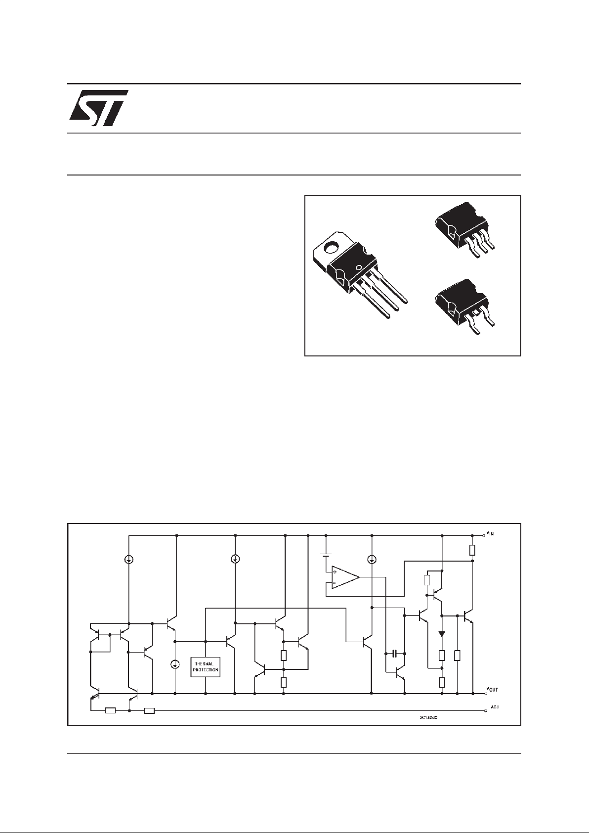
BLOCKDIAGRAM
D
2
PAK
■ TYPICALDROPOUT VOLTAGE1.3V AT3A
■ THREETERMINALADJUSTABLEOR FIXED
OUTPUTVOLATGE1.8V,2.5V,2.85V,3.3V,
3.6V,5V,8V, 9V, 12V
■ GUARANTEEDOUTPUTCURRENTUP TO
3A
■ OUTPUTTOLERANCE±1% AT 25
o
C AND
±2% IN FULLTEMPERATURERANGE
■
INTERNALPOWERAND THERMALLIMIT
■ WIDEOPERATINGTEMPERATURERANGE
-40
o
C TO 125oC
■
PACKAGEAVAILABLE:TO-220D2PAK
■ PINOUTCOMPATIBILITYWITHSTANDARD
ADJUSTABLEVOLTAGEREGULATORS
DESCRIPTION
The LD1085 is a LOW DROP Voltage Regulator
able to provide up to 3A of Output Current.
Dropout is guaranteed at a maximum of 1.5V at
the maximum output current, decreasing at
lower loads. The LD1085 is pin compatible with
older 3-terminal adjustable regulators, but has
better performances in term of drop and output
tolerance. A 2.85V output version is suitable for
SCSI-2 active termination. Unlike PNP
regulators, where a part of the output current is
wasted as quiescent current, the LD1085
quiescent current flow into the load, so increase
efficency. Only a 10µF minimum capacitor is
need for stability. The device is supplied in
TO-220, D
2
PAK and D2PAK/A packages. On
chip trimming allows the regulator to reach a
very tight output voltage tolerance, within±1%
at 25
o
C.
TO-220
D
2
PAK/A
1/15
ABSOLUTE MAXIMUM RATINGS
Symbol Parameter Value Unit
V
IN
DC InputVoltage 30 V
I
OUT
OutputCurrent Internally Limited mA
P
tot
PowerDissipation Internally Limited mW
T
stg
Storage TemperatureRange -50 to 150
o
C
T
op
OperatingJunction Temperature Range -40 to 125
o
C
Absolute Maximum Ratings are those value beyond which damage to the device may occur. Functional operation under these condition is
not implied. Over the above suggested Max Power Dissipation a ShortCircuit could definetively damage the device.
THERMALDATA
Symbol Parameter TO-220 D2PAK Unit
R
thj-cas e
R
thj-amb
Thermal Resistance Junction-case
Thermal Resistance Junction-ambient
3
50
3
62.5
o
C/W
o
C/W
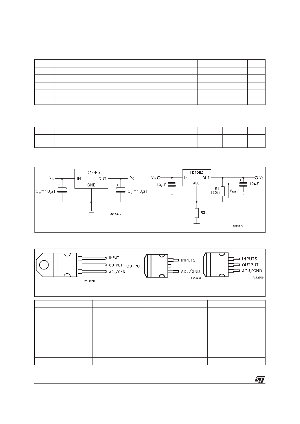
APPLICATION CIRCUIT FOR FIXED AND ADJUSTABLE VERSION
CONNECTION DIAGRAM AND ORDERING NUMBERS
(top view)
TO-220 D2PAK (**) D2PAK/A (**) Output Voltage
LD1085V18
LD1085V25
LD1085V28
LD1085V33
LD1085V36
LD1085V50
LD1085V80
LD1085V90
LD1085V120
LD1085D2T18
LD1085D2T25
LD1085D2T28
LD1085D2T33
LD1085D2T36
LD1085D2T50
LD1085D2T80
LD1085D2T90
LD1085D2T120
LD1085D2M18
LD1085D2M25
LD1085D2M28
LD1085D2M33
LD1085D2M36
LD1085D2M50
LD1085D2M80
LD1085D2M90
LD1085D2M120
1.8V
2.5V
2.85V
3.3V
3.6V
5V
8V
9V
12V
LD1085V LD1085D2T LD1085D2M 1.25 to 28V
(**)Available in Tape & Reel with the suffix ”R” for fixed version and ”-R” for adjustable version.
TO-220 D2PAK D2PAK/A
VO=
V
REF
(1 +
R
2
R
1
)
LD1085 SERIES
2/15
ELECTRICAL CHARACTERISTICS FOR LD1085#25
(refer to the test circuits,
T
j
= -40 to 125oC, VIN= 5.5 V, CIN=CO=10µF unless otherwisespecified)
Symbol Parameter Test Conditions Min. Typ. Max. Unit
V
O
OutputVoltage IO= 0 mA Tj=25oC 2.475 2.5 2.525 V
V
O
OutputVoltage(Note 1) IO= 0 to3 A Vin=4.1to 30 V 2.45 2.5 2.55 V
∆
V
O
LineRegulation Vin=4.1to 18 V IO= 0 mA Tj=25oC0.25mV
∆
V
O
LineRegulation Vin=4.1to 18 V IO=0mA 0.4 5 mV
∆
V
O
LoadRegulation IO= 0 to3 A Tj=25oC210mV
∆
V
O
LoadRegulation IO= 0 to3 A 4 20 mV
V
d
Dropout Voltage IO=3A 1.3 1.5 V
I
d
QuiescentCurrent Vin≤ 30 V 5 10 mA
I
SC
ShortCircuitCurrent VIN-VO=5V
V
IN-VO
=25V
3.2
0.2
4.5
0.5
A
Thermal Regulation T
a
=25oC 30ms Pulse 0.008 0.04 %/W
SVR Supply VoltageRejection I
O
= 3 A f= 120 Hz CO=25µF
V
in
=7.5±3V
60 72 dB
eN OutputNoise Voltage B = 10Hzto 10KHz T
a
=25oC 0.003 %
S Temperature Stability 0.5 %
S Long Term Stability 1000 hrs T
a
= 125oC0.5%
Note1: See short-circuit curve for available output current at fixed dropout.
ELECTRICAL CHARACTERISTICS FOR LD1086#18
(refer to the test circuits,
T
j
= -40 to 125oC, VIN= 4.8 V, CIN=CO=10µF unless otherwisespecified)
Symbol Parameter Test Conditions Min. Typ. Max. Unit
V
O
OutputVoltage IO= 0 mA Tj=25oC 1.782 1.8 1.818 V
V
O
OutputVoltage(Note 1) IO= 0 to3 A VIN=3.4to 30 V 1.764 1.8 1.836 V
∆
V
O
LineRegulation VIN=3.4 to18V IO= 0 mA Tj=25oC0.24mV
∆
V
O
LineRegulation VIN=3.4 to18V IO=0mA 0.4 4 mV
∆
V
O
LoadRegulation IO= 0 to3 A Tj=25oC210mV
∆
V
O
LoadRegulation IO= 0 to3 A 4 20 mV
V
d
Dropout Voltage IO=3A 1.3 1.5 V
I
d
QuiescentCurrent VIN≤ 30 V 5 10 mA
I
SC
ShortCircuitCurrent VIN-VO=5V
V
IN-VO
=25V
3.2
0.2
4.5
0.5
A
Thermal Regulation T
a
=25oC 30ms Pulse 0.008 0.04 %/W
SVR Supply VoltageRejection I
O
= 3 A f= 120 Hz CO=25µF
V
IN
=5.3±1V
60 75 dB
eN OutputNoise Voltage B = 10Hzto 10KHz T
a
=25oC 0.003 %
S Temperature Stability 0.5 %
S Long Term Stability 1000 hrs T
a
= 125oC0.5%
Note1: See short-circuit curve for available output current at fixed dropout.
LD1085 SERIES
3/15
ELECTRICAL CHARACTERISTICS FOR LD1085#285
(referto the testcircuits,
T
j
= -40 to 125oC, VIN= 5.85 V, CIN=CO=10µF unless otherwise specified)
Symbol Parameter Test Conditions Min. Typ. Max. Unit
V
O
OutputVoltage IO= 0 mA Tj=25oC 2.821 2.85 2. 879 V
V
O
OutputVoltage(Note 1) IO= 0 to3 A VIN=4.5to 30 V 2.793 2.85 2.907 V
∆
V
O
LineRegulation VIN=4.5to 18 V IO= 0 mA Tj=25oC0.26mV
∆
V
O
LineRegulation VIN=4.5to 18 V IO=0mA 0.5 6 mV
∆
V
O
LoadRegulation IO= 0 to3 A Tj=25oC315mV
∆
V
O
LoadRegulation IO= 0 to3 A 7 20 mV
V
d
Dropout Voltage IO=3A 1.3 1.5 V
I
d
QuiescentCurrent VIN≤ 30 V 5 10 mA
I
SC
ShortCircuitCurrent VIN-VO=5V
V
IN-VO
=25V
3.2
0.2
4.5
0.5
A
Thermal Regulation T
a
=25oC 30ms Pulse 0.008 0.04 %/W
SVR Supply VoltageRejection I
O
= 3 A f= 120 Hz CO=25µF
V
IN
=7.85±3V
60 72 dB
eN OutputNoise Voltage B = 10Hzto 10KHz T
a
=25oC 0.003 %
S Temperature Stability 0.5 %
S Long Term Stability 1000 hrs T
a
= 125oC0.5%
Note1: See short-circuit curve for available output current at fixed dropout.
ELECTRICAL CHARACTERISTICS FOR LD1085#33
(refer to the test circuits,
T
j
= -40 to 125oC, VIN= 6.3 V, CIN=CO=10µF unless otherwisespecified)
Symbol Parameter Test Conditions Min. Typ. Max. Unit
V
O
OutputVoltage IO= 0 mA Tj=25oC 3.267 3.3 3.333 V
V
O
OutputVoltage(Note 1) IO= 0 to3 A VIN=4.9to 30 V 3.234 3.3 3.366 V
∆
V
O
LineRegulation VIN=4.9to 18 V IO= 0 mA Tj=25oC0.56mV
∆
V
O
LineRegulation VIN=4.9to 18 V IO=0mA 1 6 mV
∆
V
O
LoadRegulation IO= 0 to3 A Tj=25oC315mV
∆
V
O
LoadRegulation IO= 0 to3 A 7 20 mV
V
d
Dropout Voltage IO=3A 1.3 1.5 V
I
d
QuiescentCurrent VIN≤ 30 V 5 10 mA
I
SC
ShortCircuitCurrent VIN-VO=5V
V
IN-VO
=25V
3.2
0.2
4.5
0.5
A
Thermal Regulation T
a
=25oC 30ms Pulse 0.008 0.04 %/W
SVR Supply VoltageRejection I
O
= 3 A f= 120 Hz CO=25µF
V
IN
=8.3±3V
60 72 dB
eN OutputNoise Voltage B = 10Hzto 10KHz T
a
=25oC 0.003 %
S Temperature Stability 0.5 %
S Long Term Stability 1000 hrs T
a
= 125oC0.5%
Note1: See short-circuit curve for available output current at fixed dropout.
LD1085 SERIES
4/15

ELECTRICAL CHARACTERISTICS FOR LD1085#36
(refer to the test circuits,
T
j
= -40 to 125oC, VIN= 5.85 V, CIN=CO=10µF unless otherwise specified)
Symbol Parameter Test Conditions Min. Typ. Max. Unit
V
O
OutputVoltage IO= 0 mA Tj=25oC 3.564 3.6 3.636 V
V
O
OutputVoltage(Note 1) IO= 0 to3 A VIN=5.2to 30 V 3.528 3.6 3.672 V
∆
V
O
LineRegulation VIN=5.2to 18 V IO= 0 mA Tj=25oC0.510mV
∆
V
O
LineRegulation VIN=5.2to 18 V IO= 0 mA 1 10 mV
∆
V
O
LoadRegulation IO= 0 to3 A Tj=25oC315mV
∆
V
O
LoadRegulation IO= 0 to3 A 7 20 mV
V
d
Dropout Voltage IO=3A 1.3 1.5 V
I
d
QuiescentCurrent VIN≤ 30 V 5 10 mA
I
SC
ShortCircuitCurrent VIN-VO=5V
V
IN-VO
=25V
3.2
0.2
4.5
0.5
A
Thermal Regulation T
a
=25oC 30ms Pulse 0.008 0.04 %/W
SVR Supply VoltageRejection I
O
= 3 A f= 120 Hz CO=25µF
V
IN
=8.6±3V
60 72 dB
eN OutputNoise Voltage B = 10Hzto 10KHz T
a
=25oC 0.003 %
S Temperature Stability 0.5 %
S Long Term Stability 1000 hrs T
a
= 125oC0.5%
Note1: See short-circuit curve for available output current at fixed dropout.
ELECTRICAL CHARACTERISTICS FOR LD1085#50
(refer to the test circuits,
T
j
= -40 to 125oC, VIN= 8 V, CIN=CO=10µF unless otherwisespecified)
Symbol Parameter Test Conditions Min. Typ. Max. Unit
V
O
OutputVoltage IO= 0 mA Tj=25oC4.9555.05V
V
O
OutputVoltage(Note 1) IO= 0 to3 A VIN=6.6to 30 V 4.9 5 5.1 V
∆
V
O
LineRegulation VIN=6.6to 20 V IO= 0 mA Tj=25oC0.510mV
∆
V
O
LineRegulation VIN=6.6to 20 V IO= 0 mA 1 10 mV
∆
V
O
LoadRegulation IO= 0 to3 A Tj=25oC520mV
∆
V
O
LoadRegulation IO= 0 to3A 10 35 m V
V
d
Dropout Voltage IO=3A 1.3 1.5 V
I
d
QuiescentCurrent VIN≤ 30 V 5 10 mA
I
SC
ShortCircuitCurrent VIN-VO=5V
V
IN-VO
=25V
3.2
0.2
4.5
0.5
A
Thermal Regulation T
a
=25oC 30ms Pulse 0.008 0.04 %/W
SVR Supply VoltageRejection I
O
= 3 A f= 120 Hz CO=25µF
V
IN
=10±3V
60 72 dB
eN OutputNoise Voltage B = 10Hzto 10KHz T
a
=25oC 0.003 %
S Temperature Stability 0.5 %
S Long Term Stability 1000 hrs T
a
= 125oC0.5%
Note1: See short-circuit curve for available output current at fixed dropout.
LD1085 SERIES
5/15

ELECTRICAL CHARACTERISTICS FOR LD1085#80
(refer to the test circuits,
T
j
= -40 to 125oC, VIN=11V, CIN=CO=10µF unlessotherwisespecified)
Symbol Parameter Test Conditions Min. Typ. Max. Unit
V
O
OutputVoltage IO= 0 mA Tj=25oC7.9288.08V
V
O
OutputVoltage(Note 1) IO= 0 to3 A VIN=9.8to 30 V 7.84 8 8.16 V
∆
V
O
LineRegulation VIN=9.8to 20 V IO= 0 mA Tj=25oC118mV
∆
V
O
LINeRegulation VIN=9.8to 20 V IO= 0 mA 2 18 mV
∆
V
O
LoadRegulation IO= 0 to3 A Tj=25oC830mV
∆
V
O
LoadRegulation IO= 0 to3A 12 60 m V
V
d
Dropout Voltage IO=3A 1.3 1.5 V
I
d
QuiescentCurrent VIN≤ 30 V 5 10 mA
I
SC
ShortCircuitCurrent VIN-VO=5V
V
IN-VO
=25V
3.2
0.2
4.5
0.5
A
Thermal Regulation T
a
=25oC 30ms Pulse 0.008 0.04 %/W
SVR Supply VoltageRejection I
O
= 3 A f= 120 Hz CO=25µF
V
IN
=13±3V
54 71 dB
eN OutputNoise Voltage B = 10Hzto 10KHz T
a
=25oC 0.003 %
S Temperature Stability 0.5 %
S Long Term Stability 1000 hrs T
a
= 125oC0.5%
Note1: See short-circuit curve for available output current at fixed dropout.
ELECTRICAL CHARACTERISTICS FOR LD1085#90
(refer to the test circuits,
T
j
= -40 to 125oC, VIN=12V, CIN=CO=10µF unlessotherwisespecified)
Symbol Parameter Test Conditions Min. Typ. Max. Unit
V
O
OutputVoltage IO= 0 mA Tj=25oC8.9199.09V
V
O
OutputVoltage(Note 1) IO= 0 to3 A VIN=11 to 30 V 8.82 9 9.18 V
∆
V
O
LineRegulation VIN=11to20V IO=0 mA Tj=25oC120mV
∆
V
O
LineRegulation VIN=11to20V IO=0 mA 2 20 mV
∆
V
O
LoadRegulation IO= 0 to3 A Tj=25oC830mV
∆
V
O
LoadRegulation IO= 0 to3A 12 60 mV
V
d
Dropout Voltage IO=3A 1.3 1.5 V
I
d
QuiescentCurrent VIN≤ 30 V 5 10 mA
I
SC
ShortCircuitCurrent VIN-VO=5V
V
IN-VO
=25V
3.2
0.2
4.5
0.5
A
Thermal Regulation T
a
=25oC 30ms Pulse 0.008 0.04 %/W
SVR Supply VoltageRejection I
O
= 3 A f= 120 Hz CO=25µF
V
IN
=14±3V
54 70 dB
eN OutputNoise Voltage B = 10Hz to 10KHz T
a
=25oC 0.003 %
S Temperature Stability 0.5 %
S Long Term Stability 1000 hrs T
a
=125oC0.5%
Note1: See short-circuit curve for available output current at fixed dropout.
LD1085 SERIES
6/15

ELECTRICAL CHARACTERISTICS FOR LD1085#120
(referto the testcircuits,
T
j
= -40 to 125oC, VIN=15V, CIN=CO=10µF unlessotherwisespecified)
Symbol Parameter Test Conditions Min. Typ. Max. Unit
V
O
OutputVoltage IO= 0 mA Tj=25oC 11.88 12 12 .1 2 V
V
O
OutputVoltage(Note 1) IO= 0 to3 A VIN=13.8to30 V 11.76 12 12.24 V
∆
V
O
LineRegulation VIN=13.8to 25 V IO= 0 mA Tj=25oC125mV
∆
V
O
LineRegulation VIN=13.8to 25 V IO= 0 mA 2 25 mV
∆
V
O
LoadRegulation IO= 0 to3 A Tj=25oC1236mV
∆
V
O
LoadRegulation IO= 0 to3A 24 72 m V
V
d
Dropout Voltage IO=3A 1.3 1.5 V
I
d
QuiescentCurrent VIN≤ 30 V 5 10 mA
I
SC
ShortCircuitCurrent VIN-VO=5V
V
IN-VO
=25V
3.2
0.2
4.5
0.5
A
Thermal Regulation T
a
=25oC 30ms Pulse 0.008 0.04 %/W
SVR Supply VoltageRejection I
O
= 3 A f= 120 Hz CO=25µF
V
IN
=17±3V
54 66 dB
eN OutputNoise Voltage B = 10Hzto 10KHz T
a
=25oC 0.003 %
S Temperature Stability 0.5 %
S Long Term Stability 1000 hrs T
a
= 125oC0.5%
Note1: See short-circuit curve for available output current at fixed dropout.
ELECTRICAL CHARACTERISTICS FOR LD1085
(refer to the test circuits,
T
j
= -40 to 125oC, VIN= 4.25 V, CIN=CO=10µF unless otherwise specified)
Symbol Parameter Test Conditions Min. Typ. Max. Unit
V
O
OutputVoltage IO=10mA Tj=25oC 1.237 1. 25 1. 263 V
V
O
OutputVoltage(Note 1) IO= 0.01 to 3 A VIN=2.8 to 30V 1.225 1.25 1.275 V
∆
V
O
LineRegulation VIN=2.75to 16.5V IO=10mA Tj=25oC 0.015 0.2 %
∆
V
O
LineRegulation VIN=2.75to 16.5V IO=10mA 0.035 0.2 %
∆
V
O
LoadRegulation IO= 0.01 to 3 A Tj=25oC0.10.3%
∆
V
O
LoadRegulation IO= 0.01 to 3 A 0.2 0.4 %
V
d
Dropout Voltage IO=3A 1.3 1.5 V
I
O(min)
MinimumLoad Current VIN=30V 3 10 mA
I
SC
ShortCircuitCurrent VIN-VO=5V
V
IN-VO
=25V
3.2
0.2
4.5
0.5
A
Thermal Regulation T
a
=25oC 30ms Pulse 0.01 0.04 %/W
SVR Supply VoltageRejection I
O
= 3 A f= 120 Hz CO=25µF
C
ADJ
=25µFVIN= 6.25±3V
60 75 dB
I
ADJ
Adjustpin Current IO=10mA VIN=4.25V 55 120 µA
∆
I
ADJ
Adjustpin Current Change VIN=2.75to 16.5 V IO=0.01to 3A 0.2 5
µ
A
eN OutputNoise Voltage B = 10Hzto 10KHz T
a
=25oC 0.003 %
S Temperature Stability 0.5 %
S Long Term Stability 1000 hrs T
a
= 125oC0.5%
Note1: See short-circuit curve for available output current at fixed dropout.
LD1085 SERIES
7/15

TYPICALCHARACTERISTICS
(unlessotherwisespecified T
J
=125oC, CIN=CO=10µF)
OutputVoltage vs Temperature OutputVoltage vs Temperature
OutputVoltage vs Temperature
Line Regulationvs Temperature
Short Circuit Current vs Dropout Voltage
LoadRegulation vs Temperature
LD1085 SERIES
8/15

DropoutVoltage vs Temperature
AdjustPin Current vs Temperature
QuiescentCurrent vs OutputCurrent
Dropout Voltage vs OutputCurrent
QuiescentCurrent vs Temperature
SupplyVoltage Rejectionvs Output Current
TYPICALCHARACTERISTICS
(Continued)
LD1085 SERIES
9/15

SupplyVoltage Rejectionvs Frequency
MinimumLoad Currentvs Temperature
Stability
SupplyVoltage Rejectionvs Temperature
Stability
TYPICALCHARACTERISTICS
(Continued)
LD1085 SERIES
10/15

Line Transient
LoadTransient
Line Transient
LoadTransient
TYPICALCHARACTERISTICS
(Continued)
LD1085 SERIES
11/15

DIM.
mm inch
MIN. TYP. MAX. MIN. TYP. MAX.
A 4.40 4.60 0.173 0.181
C 1.23 1.32 0.048 0.051
D 2.40 2.72 0.094 0.107
D1 1.27 0.050
E 0.49 0.70 0.019 0.027
F 0.61 0.88 0.024 0.034
F1 1.14 1.70 0.044 0.067
F2 1.14 1.70 0.044 0.067
G 4.95 5.15 0.194 0.203
G1 2.4 2.7 0.094 0.106
H2 10.0 10.40 0.393 0.409
L2 16.4 0.645
L4 13.0 14.0 0.511 0.551
L5 2.65 2.95 0.104 0.116
L6 15.25 15.75 0.600 0.620
L7 6.2 6.6 0.244 0.260
L9 3.5 3.93 0.137 0.154
DIA. 3.75 3.85 0.147 0.151
L6
A
C
D
E
D1
F
G
L7
L2
Dia.
F1
L5
L4
H2
L9
F2
G1
TO-220 MECHANICAL DATA
P011C
LD1085 SERIES
12/15

DIM.
mm inch
MIN. TYP. MAX. MIN. TYP. MAX.
A 4.4 4.6 0.173 0.181
A1 2.49 2.69 0.098 0.106
B 0.7 0.93 0.027 0.036
B2 1.14 1.7 0.044 0.067
C 0.45 0.6 0.017 0.023
C2 1.23 1.36 0.048 0.053
D 8.95 9.35 0.352 0.368
E 10 10.4 0.393 0.409
G 4.88 5.28 0.192 0.208
L 15 15.85 0.590 0.624
L2 1.27 1.4 0.050 0.055
L3 1.4 1.75 0.055 0.068
L2
L3
L
B2
B
G
E
A
C2
D
C
A1
DETAIL”A”
DETAIL”A”
A2
P011P6/F
TO-263 (D2PAK) MECHANICAL DATA
LD1085 SERIES
13/15

DIM.
mm inch
MIN. TYP. MAX. MIN. TYP. MAX.
A 4.4 4.6 0.173 0.181
A1 2.49 2.69 0.098 0.106
B 0.7 0.93 0.027 0.036
B2 1.14 1.7 0.044 0.067
C 0.45 0.6 0.017 0.023
C2 1.21 1.36 0.047 0.053
D 8.95 9.35 0.352 0.368
E 10 10.4 0.393 0.409
G 4.88 5.28 0.192 0.208
L 15 15.85 0.590 0.624
L2 1.27 1.4 0.050 0.055
D2PAK/A MECHANICAL DATA
LD1085 SERIES
14/15

Information furnished isbelieved tobe accurate and reliable. However, STMicroelectronics assumes no responsibility for the consequences
of use of such information nor for any infringement of patents or other rights of third parties which may result from its use. No license is
granted by implicationor otherwise under any patent or patent rights of STMicroelectronics. Specification mentioned in this publication are
subject tochange without notice. This publication supersedes and replaces all information previously supplied. STMicroelectronics products
are not authorized for use as critical components in lifesupport devices or systems withoutexpress written approval of STMicroelectronics.
The ST logo is a registeredtrademark of STMicroelectronics
2000 STMicroelectronics – Printed in Italy – All RightsReserved
STMicroelectronics GROUP OF COMPANIES
Australia - Brazil - China - Finland - France - Germany - Hong Kong - India - Italy- Japan- Malaysia - Malta - Morocco
Singapore - Spain- Sweden - Switzerland - United Kingdom - U.S.A.
http://www.st.com
.
LD1085 SERIES
15/15
 Loading...