

SGS Thomson Microelectronics LD1084V, LD1084D2T90, LD1084D2T50, LD1084D2T36, LD1084D2T33 Datasheet
...
1/18May 2003
■ TYPICAL DROPOUT 1.3V (AT 5A)
■ THREE TERMINAL ADJUSTABLE OR FIXED
OUTPUT VOLTAGE 1.5, 1.8V , 2.5V, 2.85V,
3.3V,3.6V,5V,8V,9V,12V.
■ GUARANTEED OUTPUT CURRENT UP TO
5A
■ OUPUT TOLERANCE ±1% AT 25°C AND
±2% IN FU LL TEMPERATURE RANGE
■ INTERNAL POWER AND THERMAL LIMIT
■ WIDE OPERATING TEMPERATURE RANGE
-40°C TO 125°C
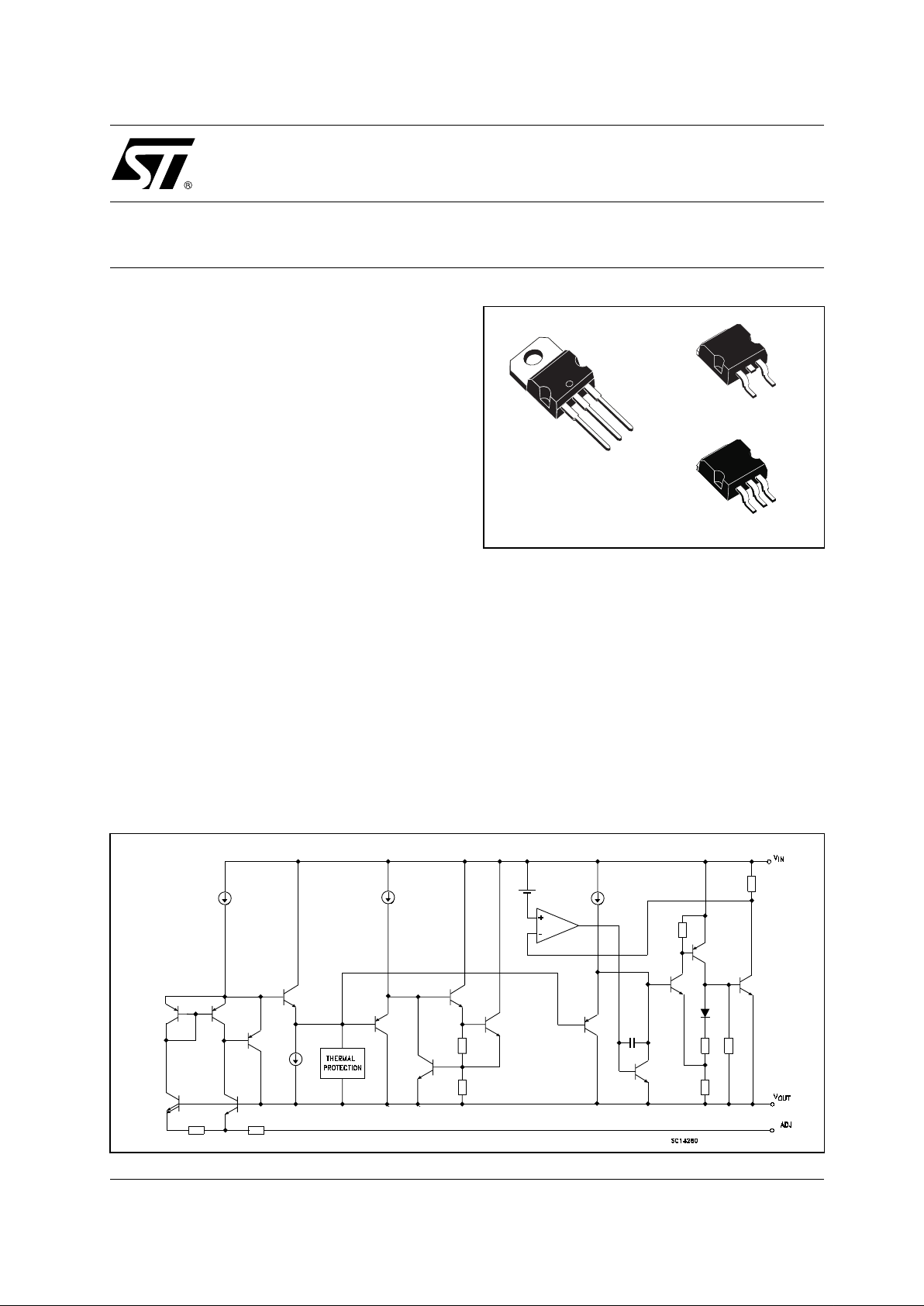
■ PACKAGE AVAILABLE : TO-220,D
2
PAK,
D
2
PAK/A
■ PINOUT COMPATIBILITY WITH STANDARD
ADJUSTABLE VREG
DESCRIPTION
The LD1084 is a LOW DROP Voltage Regulator
able to provide up to 5A of Output Current.
Dropout is guaran teed at a maxim um of 1.5V at
the maximum output current, decreasing at lower
loads. The LD1084 is pin to pin compatible with
the older 3-terminal adj us tab le regulators, but has
better performances in term of drop and output
tolerance .
A 2.85V output version is suitable for SCSI-2
active termination. Unlike PNP regulato rs, where
a part of the output current is wasted as quiescent
current, the LD1084 quiescent current flows into
the load, so increase efficiency. Only a 10µF
minimum capac it or is need for stability.
The device is supplied i n T O-220, D
2
PAK a nd
D
2
PAK/A. On chiptrimming allows the regulator to
reach a very tight output voltage tolerance, within
±1% at 25°C.
LD1084
SERIES
5A LOW DROP POSITIVE VOLTAGE
REGULATOR ADJUSTABLE AND FIXED
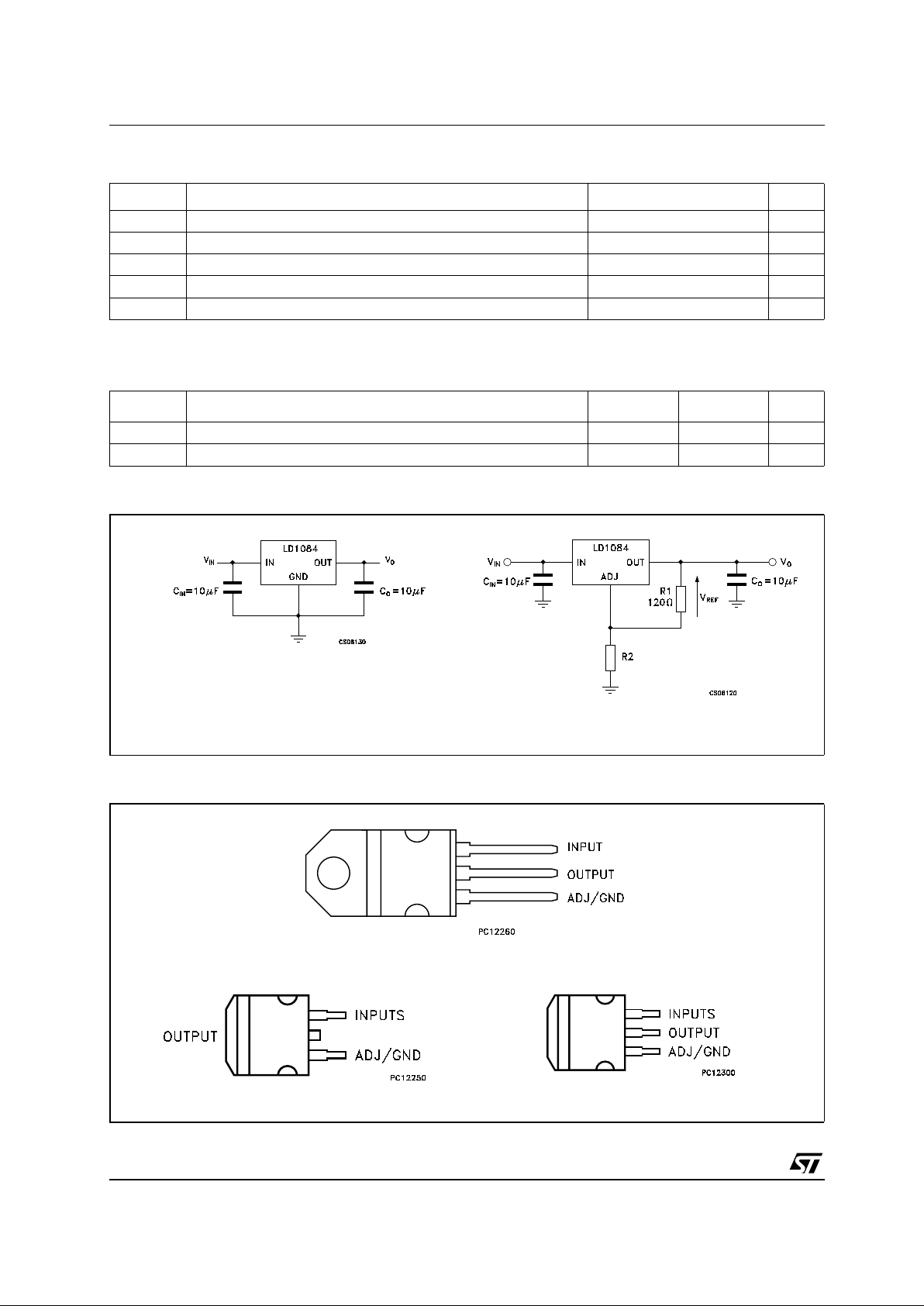
SCHEMATIC DIAGRAM
TO-220
D2PAK
D
2
PAK/A
LD1084 SERIES
2/18
ABSOLUTE MAXIMUM RATINGS
Absolute Maximum Ratings are those values beyond which damage to the device may occur. Functional operation under these condition is
not implied.
THERMAL DATA
APPLICATION CIRCUITS
CONNECTION DIAGRAM (top view)
Symbol Parameter² Value Unit
V
I
DC Input Voltage
30 V
I
O
Output Current
Internally Limited mA
P
D
Power Dissipation
Internally Limited mW
T
stg
Storage Temperature Range
-55 to +150 °C
T
op
Operating Junction Temperature Range
-40 to +125 °C
Symbol Parameter TO-220
D
2
PAK
Unit
R
thj-case
Thermal Resistance Junction-case
3 3 °C/W
R
thj-amb
Thermal Resistance Junction-ambient
50 62.5 °C/W
R
2
VO=V
REF
(1 + )
R
1
TO-220
D
2
PAK D2PAK/A
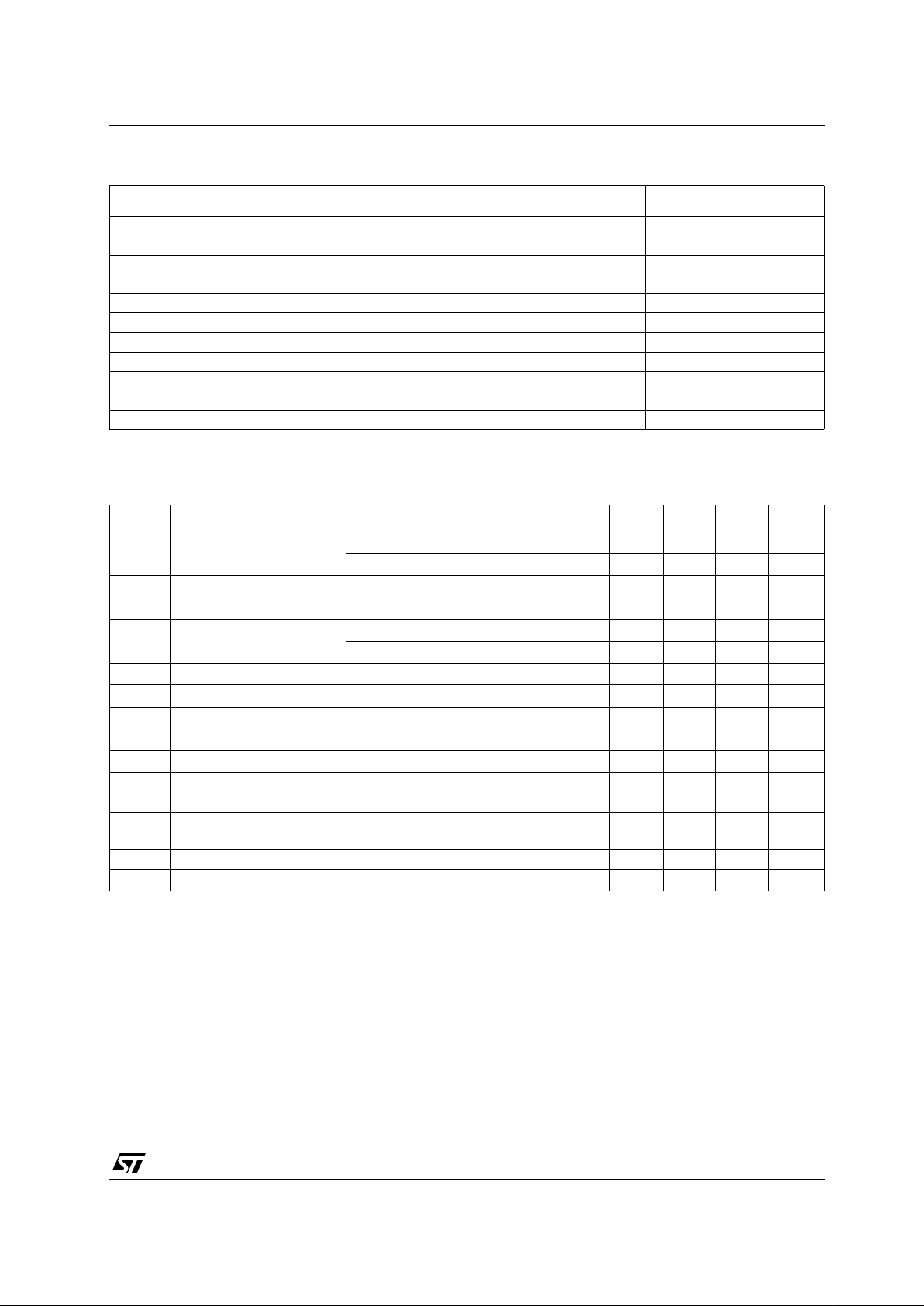
LD1084 SE RIE S
3/18
ORDERING CODES
(*) Available in Tape & Reel with the suffix "R" for fixed versions and "-R" for adjustable version
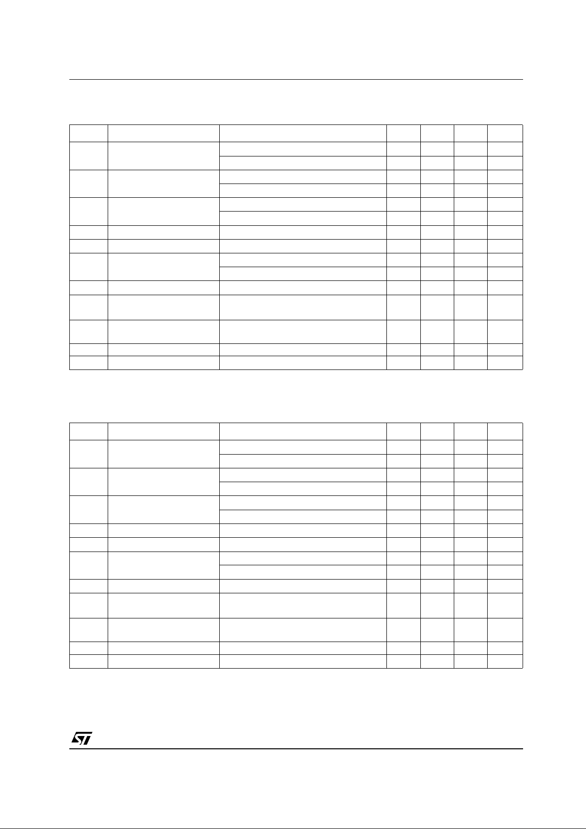
LECTRICAL CHARACTERISTICS O F L D1084#15 (VI=4.5V, CI=CO=10µF, TA= -40 to 125°C, unless
otherwise specified.)
NOTE 1: See short-circuit current curve for available output current at fixed dropout.
TYPE
D
2
PAK (*) D2PAK/A
OUTPUT VOLTAGE
LD1084V15 LD1084D2T15 LD1084D2M15 1.5 V
LD1084V18 LD1084D2T18 LD1084D2M18 1.8 V
LD1084V25 LD1084D2T25 LD1084D2M25 2.5 V
LD1084V28 LD1084D2T28 LD1084D2M28 2.85 V
LD1084V33 LD1084D2T33 LD1084D2M33 3.3 V
LD1084V36 LD1084D2T36 LD1084D2M36 3.6 V
LD1084V50 LD1084D2T50 LD1084D2M50 5.0 V
LD1084V80 LD1084D2T80 LD1084D2M80 8.0 V
LD1084V90 LD1084D2T90 LD1084D2M90 9.0 V
LD1084V120 LD1084D2T120 LD1084D2M120 12.0 V
LD1084V LD1084D2T LD1084D2M ADJ
Symbol Parameter Test Conditions Min. Typ. Max. Unit
V
O
Output Voltage IO=0mA TJ= 25°C 1.485 1.5 1.515 V
I
O
=0to5A VI= 3.1 to 30V (note 1) 1.47 1.5 1.53 V
∆V
O
Line Regulation IO=0mA VI= 3.1 to 18V TJ= 25°C 0.5 6 mV
I
O
=0mA VI= 3.1 to 15V 0.1 6 mV
∆V
O
Load Regulation IO=0to5A TJ= 25°C 3 15 mV
I
O
=0to5A 7 20 V
V
d
Dropout Voltage IO=5 A 1.3 1.5 V
I
q
Quiescent Current VI≤ 30V 5 10 mA
I
sc
Short Circuit Current VI-VO= 5V 5.5 6.5 A
V
I-VO
= 25V 0.5 0.7 A
Termal Regulation T
A
= 25°C, 30ms pulse 0.003 0.015 %/W
SVR Supply Voltage Rejection f = 120 Hz, C
O
=25µF, IO=5A
V
I
= 6.8 ± 3V
60 75 dB
eN RMS Output Noise Voltage
(% of V
O
)
T
A
= 25°C f =10Hz to 10KHz 0.003 %
S Temperature Stability 0.5 %
S Long Term Stability T
A
= 125°C 1000Hrs 0.5 %
LD1084 SERIES
4/18
ELECTRICAL CHARACTERISTICS OF LD1084#18 (VI=4.8V, CI=CO=10µF, TA= -40 to 125°C, unless
otherwise specified.)
NOTE 1: See short-circuit current curve for available output current at fixed dropout.
ELECTRICAL CHARACTERISTICS OF LD1084#25 (VI=5.5V, CI=CO=10µF, TA= -40 to 125°C, unless
otherwise specified.)
NOTE 1: See short-circuit current curve for available output current at fixed dropout.
Symbol Parameter Test Conditions Min. Typ. Max. Unit
V
O
Output Voltage IO=0mA TJ= 25°C 1.782 1.8 1.818 V
I
O
=0to5A VI= 3.4 to 30V (note 1) 1.764 1.8 1.836 V
∆V
O
Line Regulation IO=0mA VI= 3.4 to 18V TJ= 25°C 0.5 6 mV
I
O
=0mA VI= 3.4 to 15V 0.1 6 mV
∆V
O
Load Regulation IO=0to5A TJ= 25°C 3 15 mV
I
O
=0to5A 7 20 V
V
d
Dropout Voltage IO=5 A 1.3 1.5 V
I
q
Quiescent Current VI≤ 30V 5 10 mA
I
sc
Short Circuit Current VI-VO= 5V 5.5 6.5 A
V
I-VO
= 25V 0.5 0.7 A
Termal Regulation T
A
= 25°C, 30ms pulse 0.003 0.015 %/W
SVR Supply Voltage Rejection f = 120 Hz, C
O
=25µF, IO=5A
V
I
= 6.8 ± 3V
60 75 dB
eN RMS Output Noise Voltage
(% of V
O
)
T
A
= 25°C f =10Hz to 10KHz 0.003 %
S Temperature Stability 0.5 %
S Long Term Stability T
A
= 125°C 1000Hrs 0.5 %
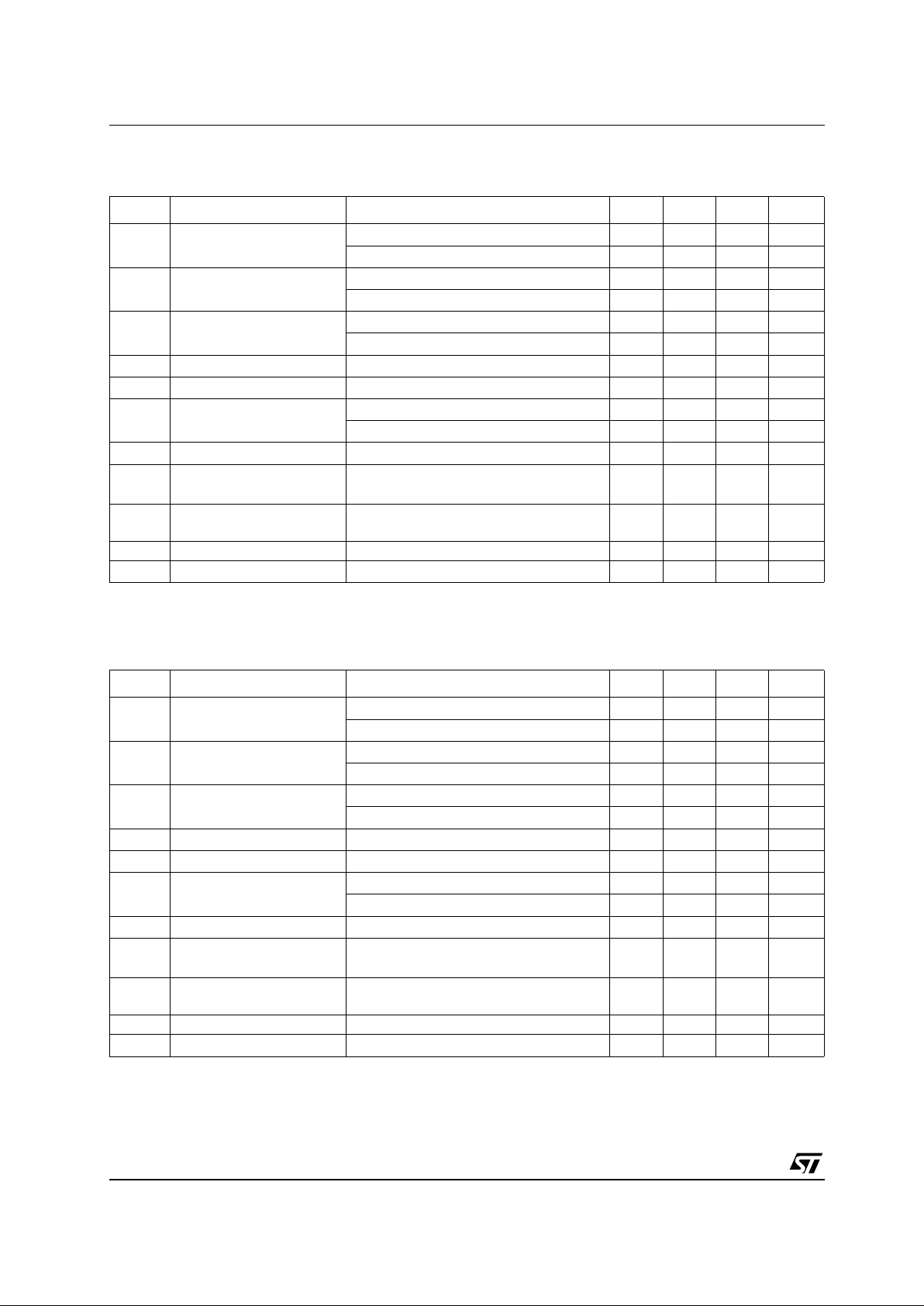
Symbol Parameter Test Conditions Min. Typ. Max. Unit
V
O
Output Voltage IO=0mA TJ= 25°C 2.475 2.5 2.525 V
I
O
=0to5A VI= 4.1 to 30V (note 1) 2.45 2.5 2.55 V
∆V
O
Line Regulation IO=0mA VI= 4.1 to 18V TJ= 25°C 0.5 6 mV
I
O
=0mA VI= 4.1 to 18V 0.1 6 mV
∆V
O
Load Regulation IO=0to5A TJ= 25°C 3 15 mV
I
O
=0to5A 7 20 V
V
d
Dropout Voltage IO=5 A 1.3 1.5 V
I
q
Quiescent Current VI≤ 30V 5 10 mA
I
sc
Short Circuit Current VI-VO= 5V 5.5 6.5 A
V
I-VO
= 25V 0.5 0.7 A
Termal Regulation T
A
= 25°C, 30ms pulse 0.003 0.015 %/W
SVR Supply Voltage Rejection f = 120 Hz, C
O
=25µF, IO=5A
V
I
= 7.5 ± 3V
60 72 dB
eN RMS Output Noise Voltage
(% of V
O
)
T
A
= 25°C f =10Hz to 10KHz 0.003 %
S Temperature Stability 0.5 %
S Long Term Stability T
A
= 125°C 1000Hrs 0.5 %
LD1084 SE RIE S
5/18
ELECTRICAL CHARACTERISTICS OF LD1084#285 (VI=5.85V, CI=CO=10µF, TA= -40 to 125°C,
unless otherwise specified. )
NOTE 1: See short-circuit current curve for available output current at fixed dropout.
ELECTRICAL CHARACTERISTICS OF LD1084#33 (VI=6.3V, CI=CO=10µF, TA= -40 to 125°C, unless
otherwise specified.)
NOTE 1: See short-circuit current curve for available output current at fixed dropout.
Symbol Parameter Test Conditions Min. Typ. Max. Unit
V
O
Output Voltage IO=0mA TJ= 25°C 2.821 2.85 2.879 V
I
O
=0to5A VI= 4.5 to 30V (note 1) 2.793 2.85 2.907 V
∆V
O
Line Regulation IO=0mA VI= 4.5 to 18V TJ= 25°C 0.5 6 mV
I
O
=0mA VI= 4.5 to 18V 0.1 6 mV
∆V
O
Load Regulation IO=0to5A TJ= 25°C 3 15 mV
I
O
=0to5A 7 20 V
V
d
Dropout Voltage IO=5 A 1.3 1.5 V
I
q
Quiescent Current VI≤ 30V 5 10 mA
I
sc
Short Circuit Current VI-VO= 5V 5.5 6.5 A
V
I-VO
= 25V 0.5 0.7 A
Termal Regulation T
A
= 25°C, 30ms pulse 0.003 0.015 %/W
SVR Supply Voltage Rejection f = 120 Hz, C
O
=25µF, IO=5A
V
I
= 7.85 ± 3V
60 72 dB
eN RMS Output Noise Voltage
(% of V
O
)
T
A
= 25°C f =10Hz to 10KHz 0.003 %
S Temperature Stability 0.5 %
S Long Term Stability T
A
= 125°C 1000Hrs 0.5 %
Symbol Parameter Test Conditions Min. Typ. Max. Unit
V
O
Output Voltage IO=0mA TJ= 25°C 3.267 3.3 3.333 V
I
O
=0to5A VI= 4.9 to 30V (note 1) 3.234 3.35 3.366 V
∆V
O
Line Regulation IO=0mA VI= 4.9 to 18V TJ= 25°C 0.5 6 mV
I
O
=0mA VI= 4.9 to 18V 0.1 6 mV
∆V
O
Load Regulation IO=0to5A TJ= 25°C 3 15 mV
I
O
=0to5A 7 20 V
V
d
Dropout Voltage IO=5 A 1.3 1.5 V
I
q
Quiescent Current VI≤ 30V 5 10 mA
I
sc
Short Circuit Current VI-VO= 5V 5.5 6.5 A
V
I-VO
= 25V 0.5 0.7 A
Termal Regulation T
A
= 25°C, 30ms pulse 0.003 0.015 %/W
SVR Supply Voltage Rejection f = 120 Hz, C
O
=25µF, IO=5A
V
I
= 8.3 ± 3V
60 72 dB
eN RMS Output Noise Voltage
(% of V
O
)
T
A
= 25°C f =10Hz to 10KHz 0.003 %
S Temperature Stability 0.5 %
S Long Term Stability T
A
= 125°C 1000Hrs 0.5 %
LD1084 SERIES
6/18
ELECTRICAL CHARACTERISTICS OF LD1084#36 (VI=6.6V, CI=CO=10µF, TA= -40 to 125°C, unless
otherwise specified.)
NOTE 1: See short-circuit current curve for available output current at fixed dropout.
ELECTRICAL CHARACTERISTICS OF LD1084#5 (VI=8V, CI=CO=10µF, TA= -40 to 125°C, unless
otherwise specified.)
NOTE 1: See short-circuit current curve for available output current at fixed dropout.
Symbol Parameter Test Conditions Min. Typ. Max. Unit
V
O
Output Voltage IO=0mA TJ= 25°C 3.564 3.6 3.636 V
I
O
=0to5A VI= 5.2 to 30V (note 1) 3.528 3.6 3.672 V
∆V
O
Line Regulation IO=0mA VI= 5.2 to 18V TJ= 25°C 0.5 10 mV
I
O
=0mA VI= 5.2 to 18V 0.1 10 mV
∆V
O
Load Regulation IO=0to5A TJ= 25°C 3 15 mV
I
O
=0to5A 7 20 V
V
d
Dropout Voltage IO=5 A 1.3 1.5 V
I
q
Quiescent Current VI≤ 30V 5 10 mA
I
sc
Short Circuit Current VI-VO= 5V 5.5 6.5 A
V
I-VO
= 25V 0.5 0.7 A
Termal Regulation T
A
= 25°C, 30ms pulse 0.003 0.015 %/W
SVR Supply Voltage Rejection f = 120 Hz, C
O
=25µF, IO=5A
V
I
= 8.6 ± 3V
60 72 dB
eN RMS Output Noise Voltage
(% of V
O
)
T
A
= 25°C f =10Hz to 10KHz 0.003 %
S Temperature Stability 0.5 %
S Long Term Stability T
A
= 125°C 1000Hrs 0.5 %
Symbol Parameter Test Conditions Min. Typ. Max. Unit
V
O
Output Voltage IO=0mA TJ= 25°C 4.95 5 5.05 V
I
O
=0to5A VI= 6.6 to 30V (note 1) 4.9 5 5.1 V
∆V
O
Line Regulation IO=0mA VI= 6.6 to 20V TJ= 25°C 0.5 10 mV
I
O
=0mA VI= 6.6 to 20V 1 10 mV
∆V
O
Load Regulation IO=0to5A TJ= 25°C 5 20 mV
I
O
=0to5A 10 35 V
V
d
Dropout Voltage IO=5 A 1.3 1.5 V
I
q
Quiescent Current VI≤ 30V 5 10 mA
I
sc
Short Circuit Current VI-VO= 5V 5.5 6.5 A
V
I-VO
= 25V 0.5 0.7 A
Termal Regulation T
A
= 25°C, 30ms pulse 0.003 0.015 %/W
SVR Supply Voltage Rejection f = 120 Hz, C
O
=25µF, IO=5A
V
I
=10± 3V
60 72 dB
eN RMS Output Noise Voltage
(% of V
O
)
T
A
= 25°C f =10Hz to 10KHz 0.003 %
S Temperature Stability 0.5 %
S Long Term Stability T
A
= 125°C 1000Hrs 0.5 %
 Loading...