

SGS Thomson Microelectronics LD1084V, LD1084D2T90, LD1084D2T50, LD1084D2T36, LD1084D2T33 Datasheet
...
1/18May 2003
■ TYPICAL DROPOUT 1.3V (AT 5A)
■ THREE TERMINAL ADJUSTABLE OR FIXED
OUTPUT VOLTAGE 1.5, 1.8V , 2.5V, 2.85V,
3.3V,3.6V,5V,8V,9V,12V.
■ GUARANTEED OUTPUT CURRENT UP TO
5A
■ OUPUT TOLERANCE ±1% AT 25°C AND
±2% IN FU LL TEMPERATURE RANGE
■ INTERNAL POWER AND THERMAL LIMIT
■ WIDE OPERATING TEMPERATURE RANGE
-40°C TO 125°C
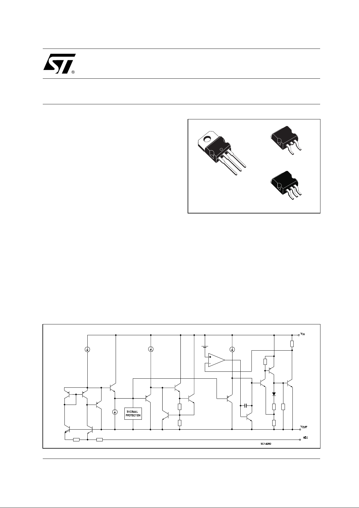
■ PACKAGE AVAILABLE : TO-220,D
2
PAK,
D
2
PAK/A
■ PINOUT COMPATIBILITY WITH STANDARD
ADJUSTABLE VREG
DESCRIPTION
The LD1084 is a LOW DROP Voltage Regulator
able to provide up to 5A of Output Current.
Dropout is guaran teed at a maxim um of 1.5V at
the maximum output current, decreasing at lower
loads. The LD1084 is pin to pin compatible with
the older 3-terminal adj us tab le regulators, but has
better performances in term of drop and output
tolerance .
A 2.85V output version is suitable for SCSI-2
active termination. Unlike PNP regulato rs, where
a part of the output current is wasted as quiescent
current, the LD1084 quiescent current flows into
the load, so increase efficiency. Only a 10µF
minimum capac it or is need for stability.
The device is supplied i n T O-220, D
2
PAK a nd
D
2
PAK/A. On chiptrimming allows the regulator to
reach a very tight output voltage tolerance, within
±1% at 25°C.
LD1084
SERIES
5A LOW DROP POSITIVE VOLTAGE
REGULATOR ADJUSTABLE AND FIXED
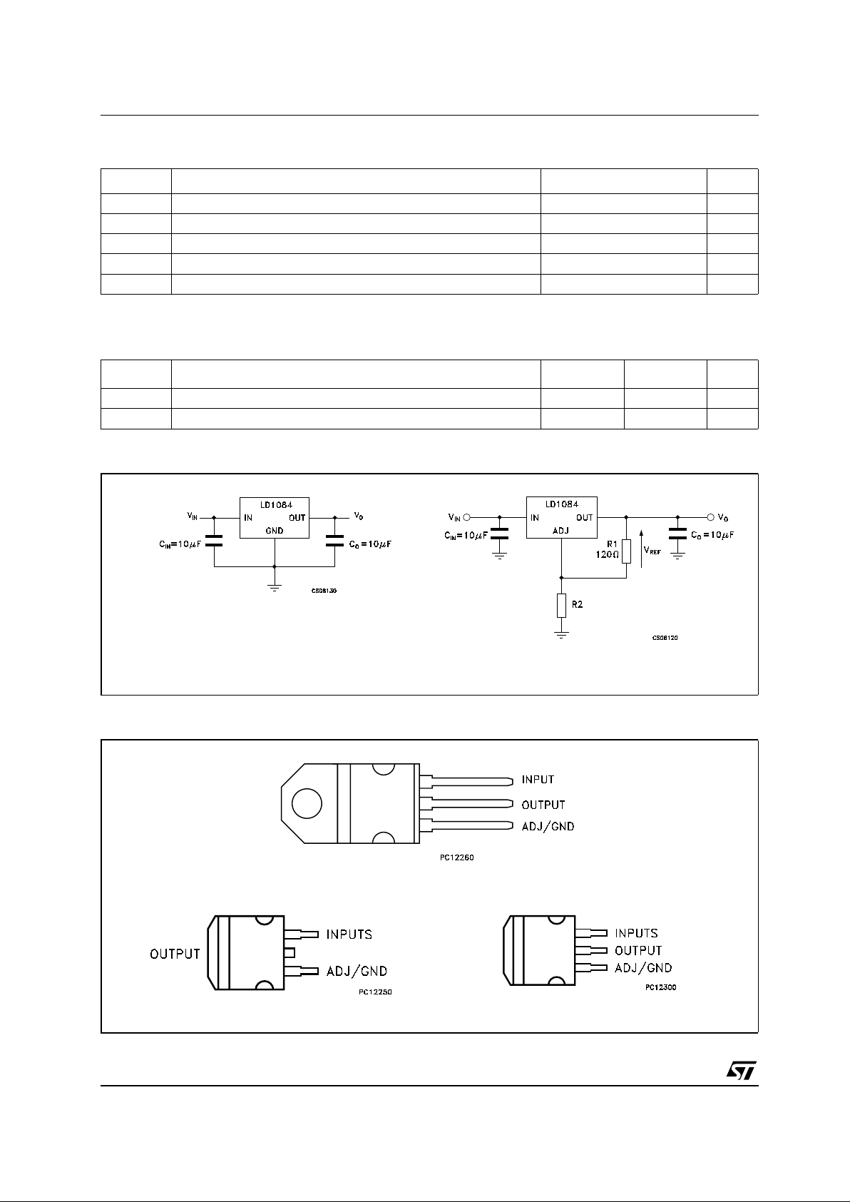
SCHEMATIC DIAGRAM
TO-220
D2PAK
D
2
PAK/A
LD1084 SERIES
2/18
ABSOLUTE MAXIMUM RATINGS
Absolute Maximum Ratings are those values beyond which damage to the device may occur. Functional operation under these condition is
not implied.
THERMAL DATA
APPLICATION CIRCUITS
CONNECTION DIAGRAM (top view)
Symbol Parameter² Value Unit
V
I
DC Input Voltage
30 V
I
O
Output Current
Internally Limited mA
P
D
Power Dissipation
Internally Limited mW
T
stg
Storage Temperature Range
-55 to +150 °C
T
op
Operating Junction Temperature Range
-40 to +125 °C
Symbol Parameter TO-220
D
2
PAK
Unit
R
thj-case
Thermal Resistance Junction-case
3 3 °C/W
R
thj-amb
Thermal Resistance Junction-ambient
50 62.5 °C/W
R
2
VO=V
REF
(1 + )
R
1
TO-220
D
2
PAK D2PAK/A
LD1084 SE RIE S
3/18
ORDERING CODES
(*) Available in Tape & Reel with the suffix "R" for fixed versions and "-R" for adjustable version
LECTRICAL CHARACTERISTICS O F L D1084#15 (VI=4.5V, CI=CO=10µF, TA= -40 to 125°C, unless
otherwise specified.)
NOTE 1: See short-circuit current curve for available output current at fixed dropout.
TYPE
D
2
PAK (*) D2PAK/A
OUTPUT VOLTAGE
LD1084V15 LD1084D2T15 LD1084D2M15 1.5 V
LD1084V18 LD1084D2T18 LD1084D2M18 1.8 V
LD1084V25 LD1084D2T25 LD1084D2M25 2.5 V
LD1084V28 LD1084D2T28 LD1084D2M28 2.85 V
LD1084V33 LD1084D2T33 LD1084D2M33 3.3 V
LD1084V36 LD1084D2T36 LD1084D2M36 3.6 V
LD1084V50 LD1084D2T50 LD1084D2M50 5.0 V
LD1084V80 LD1084D2T80 LD1084D2M80 8.0 V
LD1084V90 LD1084D2T90 LD1084D2M90 9.0 V
LD1084V120 LD1084D2T120 LD1084D2M120 12.0 V
LD1084V LD1084D2T LD1084D2M ADJ
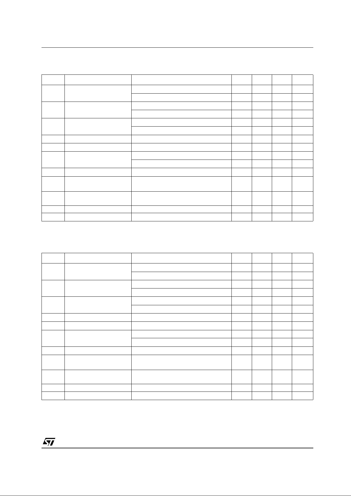
Symbol Parameter Test Conditions Min. Typ. Max. Unit
V
O
Output Voltage IO=0mA TJ= 25°C 1.485 1.5 1.515 V
I
O
=0to5A VI= 3.1 to 30V (note 1) 1.47 1.5 1.53 V
∆V
O
Line Regulation IO=0mA VI= 3.1 to 18V TJ= 25°C 0.5 6 mV
I
O
=0mA VI= 3.1 to 15V 0.1 6 mV
∆V
O
Load Regulation IO=0to5A TJ= 25°C 3 15 mV
I
O
=0to5A 7 20 V
V
d
Dropout Voltage IO=5 A 1.3 1.5 V
I
q
Quiescent Current VI≤ 30V 5 10 mA
I
sc
Short Circuit Current VI-VO= 5V 5.5 6.5 A
V
I-VO
= 25V 0.5 0.7 A
Termal Regulation T
A
= 25°C, 30ms pulse 0.003 0.015 %/W
SVR Supply Voltage Rejection f = 120 Hz, C
O
=25µF, IO=5A
V
I
= 6.8 ± 3V
60 75 dB
eN RMS Output Noise Voltage
(% of V
O
)
T
A
= 25°C f =10Hz to 10KHz 0.003 %
S Temperature Stability 0.5 %
S Long Term Stability T
A
= 125°C 1000Hrs 0.5 %
LD1084 SERIES
4/18
ELECTRICAL CHARACTERISTICS OF LD1084#18 (VI=4.8V, CI=CO=10µF, TA= -40 to 125°C, unless
otherwise specified.)
NOTE 1: See short-circuit current curve for available output current at fixed dropout.
ELECTRICAL CHARACTERISTICS OF LD1084#25 (VI=5.5V, CI=CO=10µF, TA= -40 to 125°C, unless
otherwise specified.)
NOTE 1: See short-circuit current curve for available output current at fixed dropout.
Symbol Parameter Test Conditions Min. Typ. Max. Unit
V
O
Output Voltage IO=0mA TJ= 25°C 1.782 1.8 1.818 V
I
O
=0to5A VI= 3.4 to 30V (note 1) 1.764 1.8 1.836 V
∆V
O
Line Regulation IO=0mA VI= 3.4 to 18V TJ= 25°C 0.5 6 mV
I
O
=0mA VI= 3.4 to 15V 0.1 6 mV
∆V
O
Load Regulation IO=0to5A TJ= 25°C 3 15 mV
I
O
=0to5A 7 20 V
V
d
Dropout Voltage IO=5 A 1.3 1.5 V
I
q
Quiescent Current VI≤ 30V 5 10 mA
I
sc
Short Circuit Current VI-VO= 5V 5.5 6.5 A
V
I-VO
= 25V 0.5 0.7 A
Termal Regulation T
A
= 25°C, 30ms pulse 0.003 0.015 %/W
SVR Supply Voltage Rejection f = 120 Hz, C
O
=25µF, IO=5A
V
I
= 6.8 ± 3V
60 75 dB
eN RMS Output Noise Voltage
(% of V
O
)
T
A
= 25°C f =10Hz to 10KHz 0.003 %
S Temperature Stability 0.5 %
S Long Term Stability T
A
= 125°C 1000Hrs 0.5 %
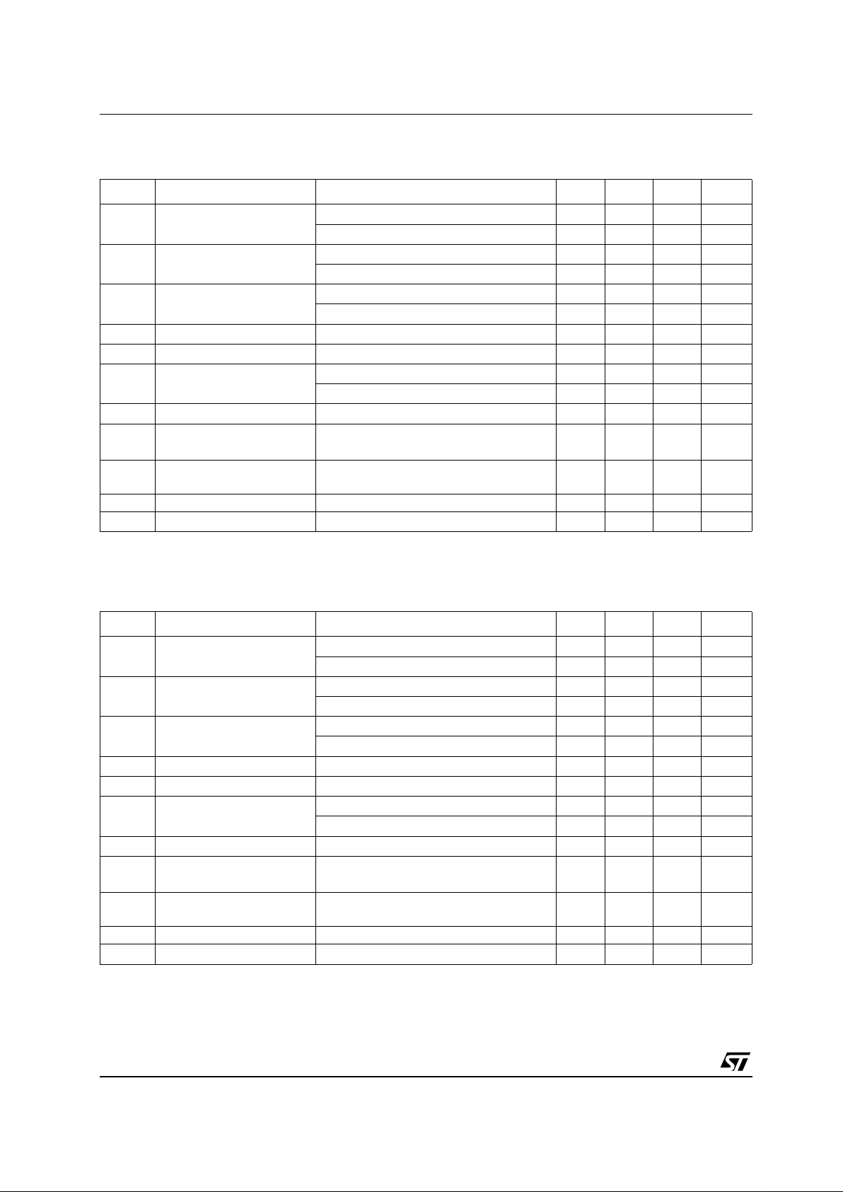
Symbol Parameter Test Conditions Min. Typ. Max. Unit
V
O
Output Voltage IO=0mA TJ= 25°C 2.475 2.5 2.525 V
I
O
=0to5A VI= 4.1 to 30V (note 1) 2.45 2.5 2.55 V
∆V
O
Line Regulation IO=0mA VI= 4.1 to 18V TJ= 25°C 0.5 6 mV
I
O
=0mA VI= 4.1 to 18V 0.1 6 mV
∆V
O
Load Regulation IO=0to5A TJ= 25°C 3 15 mV
I
O
=0to5A 7 20 V
V
d
Dropout Voltage IO=5 A 1.3 1.5 V
I
q
Quiescent Current VI≤ 30V 5 10 mA
I
sc
Short Circuit Current VI-VO= 5V 5.5 6.5 A
V
I-VO
= 25V 0.5 0.7 A
Termal Regulation T
A
= 25°C, 30ms pulse 0.003 0.015 %/W
SVR Supply Voltage Rejection f = 120 Hz, C
O
=25µF, IO=5A
V
I
= 7.5 ± 3V
60 72 dB
eN RMS Output Noise Voltage
(% of V
O
)
T
A
= 25°C f =10Hz to 10KHz 0.003 %
S Temperature Stability 0.5 %
S Long Term Stability T
A
= 125°C 1000Hrs 0.5 %
LD1084 SE RIE S
5/18
ELECTRICAL CHARACTERISTICS OF LD1084#285 (VI=5.85V, CI=CO=10µF, TA= -40 to 125°C,
unless otherwise specified. )
NOTE 1: See short-circuit current curve for available output current at fixed dropout.
ELECTRICAL CHARACTERISTICS OF LD1084#33 (VI=6.3V, CI=CO=10µF, TA= -40 to 125°C, unless
otherwise specified.)
NOTE 1: See short-circuit current curve for available output current at fixed dropout.
Symbol Parameter Test Conditions Min. Typ. Max. Unit
V
O
Output Voltage IO=0mA TJ= 25°C 2.821 2.85 2.879 V
I
O
=0to5A VI= 4.5 to 30V (note 1) 2.793 2.85 2.907 V
∆V
O
Line Regulation IO=0mA VI= 4.5 to 18V TJ= 25°C 0.5 6 mV
I
O
=0mA VI= 4.5 to 18V 0.1 6 mV
∆V
O
Load Regulation IO=0to5A TJ= 25°C 3 15 mV
I
O
=0to5A 7 20 V
V
d
Dropout Voltage IO=5 A 1.3 1.5 V
I
q
Quiescent Current VI≤ 30V 5 10 mA
I
sc
Short Circuit Current VI-VO= 5V 5.5 6.5 A
V
I-VO
= 25V 0.5 0.7 A
Termal Regulation T
A
= 25°C, 30ms pulse 0.003 0.015 %/W
SVR Supply Voltage Rejection f = 120 Hz, C
O
=25µF, IO=5A
V
I
= 7.85 ± 3V
60 72 dB
eN RMS Output Noise Voltage
(% of V
O
)
T
A
= 25°C f =10Hz to 10KHz 0.003 %
S Temperature Stability 0.5 %
S Long Term Stability T
A
= 125°C 1000Hrs 0.5 %
Symbol Parameter Test Conditions Min. Typ. Max. Unit
V
O
Output Voltage IO=0mA TJ= 25°C 3.267 3.3 3.333 V
I
O
=0to5A VI= 4.9 to 30V (note 1) 3.234 3.35 3.366 V
∆V
O
Line Regulation IO=0mA VI= 4.9 to 18V TJ= 25°C 0.5 6 mV
I
O
=0mA VI= 4.9 to 18V 0.1 6 mV
∆V
O
Load Regulation IO=0to5A TJ= 25°C 3 15 mV
I
O
=0to5A 7 20 V
V
d
Dropout Voltage IO=5 A 1.3 1.5 V
I
q
Quiescent Current VI≤ 30V 5 10 mA
I
sc
Short Circuit Current VI-VO= 5V 5.5 6.5 A
V
I-VO
= 25V 0.5 0.7 A
Termal Regulation T
A
= 25°C, 30ms pulse 0.003 0.015 %/W
SVR Supply Voltage Rejection f = 120 Hz, C
O
=25µF, IO=5A
V
I
= 8.3 ± 3V
60 72 dB
eN RMS Output Noise Voltage
(% of V
O
)
T
A
= 25°C f =10Hz to 10KHz 0.003 %
S Temperature Stability 0.5 %
S Long Term Stability T
A
= 125°C 1000Hrs 0.5 %
LD1084 SERIES
6/18
ELECTRICAL CHARACTERISTICS OF LD1084#36 (VI=6.6V, CI=CO=10µF, TA= -40 to 125°C, unless
otherwise specified.)
NOTE 1: See short-circuit current curve for available output current at fixed dropout.
ELECTRICAL CHARACTERISTICS OF LD1084#5 (VI=8V, CI=CO=10µF, TA= -40 to 125°C, unless
otherwise specified.)
NOTE 1: See short-circuit current curve for available output current at fixed dropout.
Symbol Parameter Test Conditions Min. Typ. Max. Unit
V
O
Output Voltage IO=0mA TJ= 25°C 3.564 3.6 3.636 V
I
O
=0to5A VI= 5.2 to 30V (note 1) 3.528 3.6 3.672 V
∆V
O
Line Regulation IO=0mA VI= 5.2 to 18V TJ= 25°C 0.5 10 mV
I
O
=0mA VI= 5.2 to 18V 0.1 10 mV
∆V
O
Load Regulation IO=0to5A TJ= 25°C 3 15 mV
I
O
=0to5A 7 20 V
V
d
Dropout Voltage IO=5 A 1.3 1.5 V
I
q
Quiescent Current VI≤ 30V 5 10 mA
I
sc
Short Circuit Current VI-VO= 5V 5.5 6.5 A
V
I-VO
= 25V 0.5 0.7 A
Termal Regulation T
A
= 25°C, 30ms pulse 0.003 0.015 %/W
SVR Supply Voltage Rejection f = 120 Hz, C
O
=25µF, IO=5A
V
I
= 8.6 ± 3V
60 72 dB
eN RMS Output Noise Voltage
(% of V
O
)
T
A
= 25°C f =10Hz to 10KHz 0.003 %
S Temperature Stability 0.5 %
S Long Term Stability T
A
= 125°C 1000Hrs 0.5 %
Symbol Parameter Test Conditions Min. Typ. Max. Unit
V
O
Output Voltage IO=0mA TJ= 25°C 4.95 5 5.05 V
I
O
=0to5A VI= 6.6 to 30V (note 1) 4.9 5 5.1 V
∆V
O
Line Regulation IO=0mA VI= 6.6 to 20V TJ= 25°C 0.5 10 mV
I
O
=0mA VI= 6.6 to 20V 1 10 mV
∆V
O
Load Regulation IO=0to5A TJ= 25°C 5 20 mV
I
O
=0to5A 10 35 V
V
d
Dropout Voltage IO=5 A 1.3 1.5 V
I
q
Quiescent Current VI≤ 30V 5 10 mA
I
sc
Short Circuit Current VI-VO= 5V 5.5 6.5 A
V
I-VO
= 25V 0.5 0.7 A
Termal Regulation T
A
= 25°C, 30ms pulse 0.003 0.015 %/W
SVR Supply Voltage Rejection f = 120 Hz, C
O
=25µF, IO=5A
V
I
=10± 3V
60 72 dB
eN RMS Output Noise Voltage
(% of V
O
)
T
A
= 25°C f =10Hz to 10KHz 0.003 %
S Temperature Stability 0.5 %
S Long Term Stability T
A
= 125°C 1000Hrs 0.5 %

LD1084 SE RIE S
7/18
ELECTRICAL CHARACTERISTICS OF LD1084#8 (VI=11V, CI=CO=10µF, TA= -40 to 125°C, unless
otherwise specified.)
NOTE 1: See short-circuit current curve for available output current at fixed dropout.
ELECTRICAL CHARACTERISTICS OF LD1084#9 (VI=12V, CI=CO=10µF, TA= -40 to 125°C, unless
otherwise specified.)
NOTE 1: See short-circuit current curve for available output current at fixed dropout.
Symbol Parameter Test Conditions Min. Typ. Max. Unit
V
O
Output Voltage IO=0mA TJ= 25°C 7.92 8 8.08 V
I
O
=0to5A VI= 9.6 to 30V (note 1) 7.84 8 8.16 V
∆V
O
Line Regulation IO=0mA VI= 9.6 to 20V TJ= 25°C 1 18 mV
I
O
=0mA VI= 9.6 to 20V 2 18 mV
∆V
O
Load Regulation IO=0to5A TJ= 25°C 8 30 mV
I
O
=0to5A 12 60 V
V
d
Dropout Voltage IO=5 A 1.3 1.5 V
I
q
Quiescent Current VI≤ 30V 5 10 mA
I
sc
Short Circuit Current VI-VO= 5V 5.5 6.5 A
V
I-VO
= 25V 0.5 0.7 A
Termal Regulation T
A
= 25°C, 30ms pulse 0.003 0.015 %/W
SVR Supply Voltage Rejection f = 120 Hz, C
O
=25µF, IO=5A
V
I
=13± 3V
54 71 dB
eN RMS Output Noise Voltage
(% of V
O
)
T
A
= 25°C f =10Hz to 10KHz 0.003 %
S Temperature Stability 0.5 %
S Long Term Stability T
A
= 125°C 1000Hrs 0.5 %
Symbol Parameter Test Conditions Min. Typ. Max. Unit
V
O
Output Voltage IO=0mA TJ= 25°C 8.91 9 9.09 V
I
O
=0to5A VI= 10.6 to 30V (note 1) 8.82 9 9.18 V
∆V
O
Line Regulation IO=0mA VI=10.6to20V TJ= 25°C 1 20 mV
I
O
=0mA VI=10.6to20V 2 20 mV
∆V
O
Load Regulation IO=0to5A TJ= 25°C 8 30 mV
I
O
=0to5A 12 60 V
V
d
Dropout Voltage IO=5 A 1.3 1.5 V
I
q
Quiescent Current VI≤ 30V 5 10 mA
I
sc
Short Circuit Current VI-VO= 5V 5.5 6.5 A
V
I-VO
= 25V 0.5 0.7 A
Termal Regulation T
A
= 25°C, 30ms pulse 0.003 0.015 %/W
SVR Supply Voltage Rejection f = 120 Hz, C
O
=25µF, IO=5A
V
I
=14± 3V
54 70 dB
eN RMS Output Noise Voltage
(% of V
O
)
T
A
= 25°C f =10Hz to 10KHz 0.003 %
S Temperature Stability 0.5 %
S Long Term Stability T
A
= 125°C 1000Hrs 0.5 %

LD1084 SERIES
8/18
ELECTRICAL CHARACT E R ISTICS OF LD1084# 120 (VI=15V, CI=CO=10µF,TA= -40 to125°C, unless
otherwise specified.)
NOTE 1: See short-circuit current curve for available output current at fixed dropout.
ELECTRICAL CHARACTERISTICS OF LD1084 (VI=4.25V, CI=CO=10µF, TA= -40 to 125°C, unless
otherwise specified.)
NOTE 1: See short-circuit current curve for available output current at fixed dropout.
Symbol Parameter Test Conditions Min. Typ. Max. Unit
V
O
Output Voltage IO=0mA TJ= 25°C 11.88 12 12.12 V
I
O
=0to5A VI= 13.6 to 30V (note 1) 11.76 12 12.24 V
∆V
O
Line Regulation IO=0mA VI=13.6to25V TJ= 25°C 2 25 mV
I
O
=0mA VI=13.6to25V 4 25 mV
∆V
O
Load Regulation IO=0to5A TJ= 25°C 12 36 mV
I
O
=0to5A 24 72 V
V
d
Dropout Voltage IO=5 A 1.3 1.5 V
I
q
Quiescent Current VI≤ 30V 5 10 mA
I
sc
Short Circuit Current VI-VO= 5V 5.5 6.5 A
V
I-VO
= 25V 0.5 0.7 A
Termal Regulation T
A
= 25°C, 30ms pulse 0.003 0.015 %/W
SVR Supply Voltage Rejection f = 120 Hz, C
O
=25µF, IO=5A
V
I
=17± 3V
54 66 dB
eN RMS Output Noise Voltage
(% of V
O
)
T
A
= 25°C f =10Hz to 10KHz 0.003 %
S Temperature Stability 0.5 %
S Long Term Stability T
A
= 125°C 1000Hrs 0.5 %
Symbol Parameter Test Conditions Min. Typ. Max. Unit
V
O
Output Voltage IO= 10mA TJ= 25°C 1.237 1.25 1.263 V
I
O
= 10mA to 5A VI= 2.85 to 30V
(note 1)
1.225 1.25 1.275 V
∆V
O
Line Regulation IO= 10mA VI= 2.85 to 16.5V TJ= 25°C 0.015 0.2 %
I
O
= 10mA VI= 2.85 to 16.5V 0.035 0.2 %
∆V
O
Load Regulation IO= 10mA to 5A TJ= 25°C 0.1 0.3 %
I
O
= 10mA to 5A 0.2 0.4 %
V
d
Dropout Voltage IO= 5A 1.3 1.5 V
I
O(min)
Minimum Load Current VI= 30V 3 10 mA
I
sc
Short Circuit Current VI-VO= 5V 5.5 6.5 A
V
I-VO
= 25V 0.5 0.7 A
Termal Regulation T
A
= 25°C, 30ms pulse 0.003 0.015 %/W
SVR Supply Voltage Rejection f = 120 Hz, C
O
=25µF, C
ADJ
=25µF,
I
O
=5A VI= 6.25 ± 3V
60 72 dB
I
ADJ
Adjust Pin Current VI= 4.25V IO=10mA 55 120 µA
∆I
ADJ
Adjust Pin Current Change IO= 10mA to 5A VI= 2.85 to 16.5V
(note 1)
0.2 5 µA
eN RMS Output Noise Voltage
(% of V
O
)
T
A
= 25°C f =10Hz to 10KHz 0.003 %
S Temperature Stability 0.5 %
S Long Term Stability T
A
= 125°C 1000Hrs 0.5 %

LD1084 SE RIE S
9/18
TYPICAL CHARACTERISTICS
(unless otherwise specified Tj= 25°C, CI=10µF (tant.), CO=22µF (tant.)
Figure1 : S hort Circuit Current vs Dropout
Voltage
Figure2 : Line Regulation vs Temperat ure
Figure3 : Quiescent Current vs Temp eratu re
Figure4 : Output Voltage vs Temperature
Figure5 : Load Regulation vs Tem perat ure
Figure6 : Quiescent Current vs Outpu t Voltage

LD1084 SERIES
10/18
Figure7 : Quiescent Current vs Input V oltage
Figure8 : Dropout Voltage vs Outpu t Current
Figure9 : S upply V oltage Rejection vs Output
Current
Figure10 : Dropout Voltage vs Temperature
Figure11 : Supply Vol tag e Rejection v s
Temperature
Figure12 : Supply Vol tag e Rejection v s
Frequency

LD1084 SE RIE S
11/18
Figure13 : Adjust Pin Current vs Output Current
Figure14 : Reference Voltage vs Temperature
Figure15 : Load Regulation vs Temperature
Figure16 : Adjust Pin Current vs Temperature
Figure17 : Line Regul ation vs Temperature
Figure18 : Minimum Load Currennt vs
Temperature

LD1084 SERIES
12/18
Figure19 : Supply Vol tag e Rejection v s
Temperature
Figure20 : Supply Vol tag e Rejection v s
Frequency
Figure21 : Stability
Figure22 : Supply Vol tag e Rejection v s Output
Current
Figure23 : Stability
Figure24 : Line Transient
V
I
=14to15V,
I
O
=
200mA,C
I
=1µF(tant),
C
O
=10µF(tant),ts=tf=5µs

LD1084 SE RIE S
13/18
Figure25 : Line Transient
Figure26 : Load Trans ient
Figure27 : Load Trans ient
Figure28 : Line Transient
Figure29 : Load Trans ient
V
I
=12to
13V,I
O
=
200mA,C
I
=1µF(tant),
C
O
=10µF(tant),No
C
ADJ
ts=tf=5µs
V
I
=15V,
I
O
=0.1to 5A,
C
I
=1µF(tant),
C
O
=10µF(tant
)
V
I
=
15 V,I
O
=0.1to5A,
C
I
=1µ
F(tant),C
O
=10µ
F(tant),NoC
ADJ
V
I
=12to
13V,I
O
=
200mA,C
I
=1µF(tant),
C
O
=10µF(tant),
C
ADJ
=1µFts=tf=5µs
V
I
=
13 V,I
O
=0.1to5A,
C
I
=1µ
F(tant),C
O
=10µ
F(tant)

LD1084 SERIES
14/18
DIM.
mm. inch
MIN. TYP MAX. MIN. TYP. MAX.
A 4.40 4.60 0.173 0.181
C 1.23 1.32 0.048 0.051
D 2.40 2.72 0.094 0.107
D1 1.27 0.050
E 0.49 0.70 0.019 0.027
F 0.61 0.88 0.024 0.034
F1 1.14 1.70 0.044 0.067
F2 1.14 1.70 0.044 0.067
G 4.95 5.15 0.194 0.203
G1 2.4 2.7 0.094 0.106
H2 10.0 10.40 0.393 0.409
L2 16.4 0.645
L4 13.0 14.0 0.511 0.551
L5 2.65 2.95 0.104 0.116
L6 15.25 15.75 0.600 0.620
L7 6.2 6.6 0.244 0.260
L9 3.5 3.93 0.137 0.154
DIA. 3.75 3.85 0.147 0.151
TO-220 MECHANICAL DAT
A
P011C

LD1084 SE RIE S
15/18
DIM.
mm. inch
MIN. TYP MAX. MIN. TYP. MAX.
A 4.4 4.6 0.173 0.181
A1 2.49 2.69 0.098 0.106
A2 0.03 0.23 0.001 0.009
B 0.7 0.93 0.027 0.036
B2 1.14 1.7 0.044 0.067
C 0.45 0.6 0.017 0.023
C2 1.23 1.36 0.048 0.053
D 8.95 9.35 0.352 0.368
D1 8 0.315
E 10 10.4 0.393 0.409
E1 8.5 0.335
G 4.88 5.28 0.192 0.208
L 15 15.85 0.590 0.624
L2 1.27 1.4 0.050 0.055
L3 1.4 1.75 0.055 0.068
M 2.4 3.2 0.094 0.126
R 0.4 0.016
V2 0˚ 8˚ 0˚ 8˚
D2PAK MEC
HANICAL DATA
P011P6G

LD1084 SERIES
16/18
DIM.
mm. inch
MIN. TYP MAX. MIN. TYP. MAX.
A 4.40 4.60 0.173 0.181
A1 2.49 2.69 0.098 0.106
B 0.7 0.93 0.027 0.036
B2 1.14 1.7 0.044 0.067
C 0.45 0.60 0.017 0.023
C2 1.21 1.36 0.047 0.053
D 8.95 9.35 0.352 0.368
E 10 10.4 0.393 0.409
G 4.88 5.28 0.192 0.208
L 15 15.85 0.590 0.106
L2 1.27 1.4 0.050 0.055
D2PAK/A MECHA
NICAL DATA

LD1084 SERIES
17/18
DIM.
mm. inch
MIN. TYP MAX. MIN. TYP. MAX.
A 180 7.086
C 12.8 13.0 13.2 0.504 0.512 0.519
D 20.2 0.795
N 60 2.362
T 14.4 0.567
Ao 10.50 10.6 10.70 0.413 0.417 0.421
Bo 15.70 15.80 15.90 0.618 0.622 0.626
Ko 4.80 4.90 5.00 0.189 0.193 0.197
Po 3.9 4.0 4.1 0.153 0.157 0.161
P 11.9 12.0 12.1 0.468 0.472 0.476
Tape & Reel D
2
PAK-P2PAK-D2PAK/A-P2PAK/A MECHANICAL DATA

LD1084 SERIES
18/18
Information furnished is believed to be accurate and reliable. However, STMicroelectronics assumes no responsibility for the
consequences of use o f suc h inf ormat ion n or f or an y infr ingeme nt of paten ts or oth er ri gh ts of third part ies whic h may resul t f rom
its use. No license is granted by implication or otherwise under any patent or patent rights of STMicroelectronics. Specifications
mentioned in this publication are subject to change without notice. This publication supersedes and replaces all information
previously supplied. STMicroelectronics products are not authorized for use as critical components in life support devices or
systems without express written approval of STMicroelectronics.
© The ST logo is a registered trademark of STMicroelectronics
© 2003 STMicroelectronics - Printed in Italy - All Rights Reserved
STMicroelectronics GROUP OF COMPANIES
Australia - Brazil - Canada - China - Finland - France - Germany - Hong Kong - India - Israel - Italy - Japan - Malaysia - Malta - Morocco
Singapore - Spain - Sweden - Switzerland - United Kingdom - United States.
© http://www.st.com
 Loading...