

®
LCP1521
Appl icat ion Sp ecif ic Dis cret es
A.S.D.
FEATURES
Dual programmable transient suppressor
Wide negative firing voltage range:
V
= -150 V max.
MGL
Low dynamic switching voltages: VFP and V
Low gate triggering current: IGT = 2 mA max
Peak pulse current: IPP = 30 A (10/1000 µs)
Holding current: IH = 150 mA
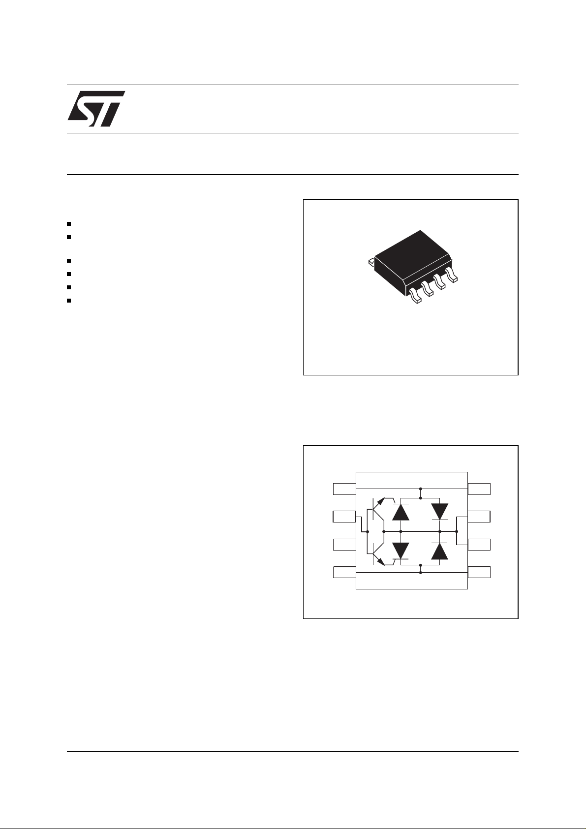
DESCRIPTION
This device has been especially designed to protect new high voltage, as well as classical SLICs,
against transient overvoltages.
Positive overvoltages are clipped with 2 diodes.
Negative surges are suppressed by 2 thyristors, their breakdown voltage being referenced
to -V
This component presents a very low gate triggering current (I
sumption on printed circuit board during the firing
phase.
A particular attention has been given to the internal
wire bonding. The K elvin method c onfiguration ensures reliable protection, reducing the overvoltage
introduced by the parasitic inductances of the wiring L x(dI/dt), especially for very fast transients.
through the gate.
BAT
) in order to reduce the current con-
GT
TM
DGL
PROGRAMMABLE TRANSIENT VOLTAGE
SUPPRESSOR FOR SLIC PROTECTION
SO-8
FUNCTIONAL DIAGRAM
TIP
GA TE
NC
RING
TIP
GND
GND
RING
September 1999 - Ed: 2A
1/9
LCP1521
COMPLIES WITH THE
FOLLOWING STANDARDS:
ITU-T K20
VDE0433
VDE0878
IEC1000-4-5
FCC Part 68
lightning surge type A
FCC Part 68
Peak Surge
Voltage
(V)
4000
1000
Voltage
Waveform
(µs)
10/700
10/700
Current
Waveform
(µs)
5/310
5/310
Admissible
Ipp
(A)
40
25
2000 10/700 5/310 40 10
2000 1.2/50 1/20 50 2
level 3
level 4
1500
800
10/700
1.2/50
10/160
10/560
5/310
8/20
10/160
10/560
40
100
50
35
1000 9/720 5/320 25 -
Necessary
Resistor
(Ω)
lightning surge type B
BELLCORE:
NWT-001089-CORE
2500
1000
2/10
10/1000
2/10
10/1000
170
30
First level
BELLCORE:
5000 2/10 2/10 170 20
NWT-001089-CORE
Second level
Note 1:
the mentioned value of the series resistance is the minimum value needed to fulfill the standard r equirement.
ABSOL UTE M AXIMU M RA TIN GS
= 25°C, unless otherwise specified).
(T
amb
Symbol Parameter Value Unit
I
PP
I
TSM
I
GSM
V
MLG
V
MGL
T
stg
Tj
T
L
Peak pulse current (see note1)
Non repetitive surge peak on-state curr ent
(F = 50Hz)
Maximum gate current (half sine wave tp = 10ms)
Maximum voltage LINE/GND
Maximum voltage GATE/LINE
Storage temperature range
Maximum junction temperature
Maximum lead temperature for soldering d uring 10s
10/1000µs
5/310µs
2/10µs
tp = 10ms
t = 1s
-40° C < Tamb < +85°C
-40° C < Tamb < +85°C
30
40
170
20
5
2A
-150
-150
- 55 to + 150
150
260
60
10
22
15
10
24
-
-
A
A
V
°
C
°
C
Note 1 :
2/9
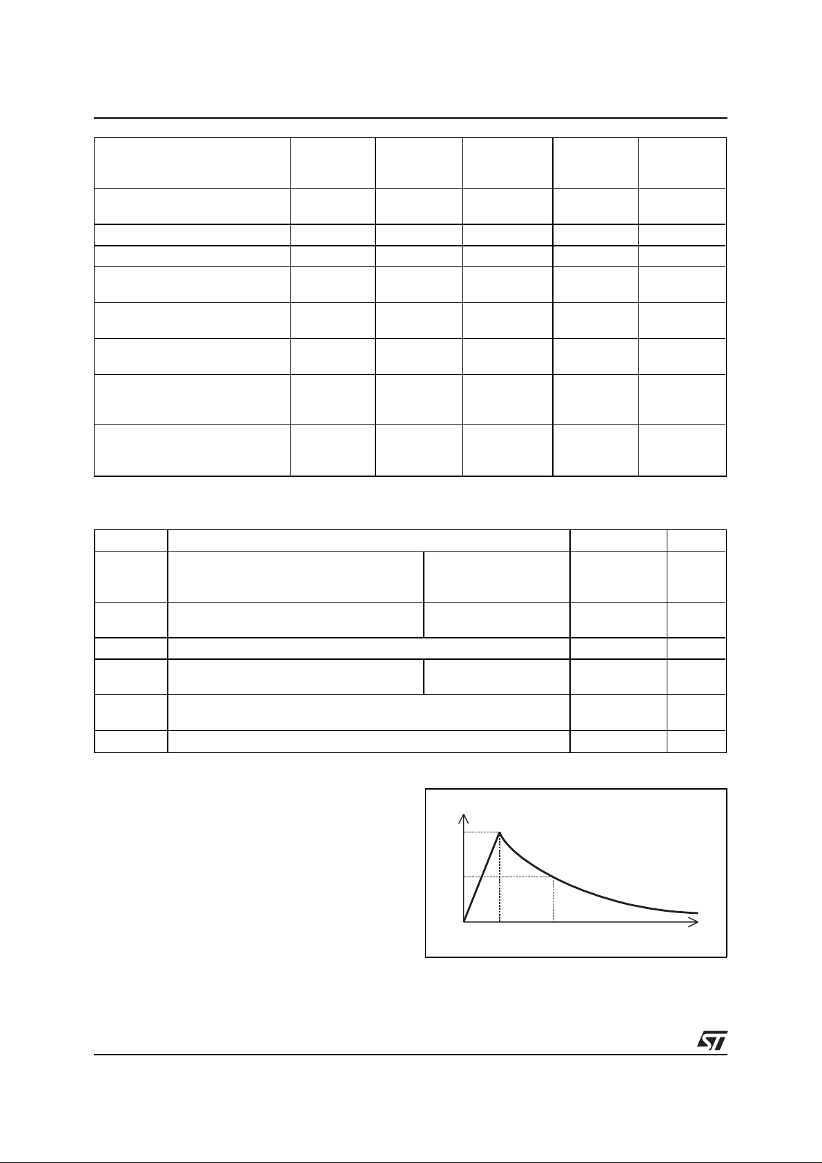
Pulse waveform
10 / 1000 µs tr = 10 µs tp = 1000 µs
5 / 310 µstr = 5
2 / 10 µstr = 2
µ
s tp = 310 µs
µ
s tp = 10 µs
100
50
%I
0
PP
t
r
t
p
t
LCP1521
THERMAL RESISTANCE
Symbol Parameter Value Unit
Rth (j-a)
Junction to ambient
170
°
C/W
ELECTRICAL CHARACTERISTICS
(T
amb
= 25°C)
Symbol Parameter
I
GT
I
H
I
RM
I
RG
V
RM
V
GT
V
V
FP
V
DGL
V
GATE
V
RG
C
1 - PARAMETERS RELATED TO THE DIODE LINE / GND
Gate triggering current
Holding current
Reverse leakage current LINE / GND
Reverse leakage current GATE / LINE
Reverse voltage LINE / GND
Gate triggering voltage
Forward drop voltage LINE / GND
F
Peak forward voltage LINE / GND
Dynamic switching voltage GATE / LINE
GATE / GND voltage
Reverse voltage GATE / LINE
Capacitance LINE / GND
(T
V
amb
DGL
V
V
R
= 25°C)
RM
V
F
I
RM
I
R
I
H
I
PP
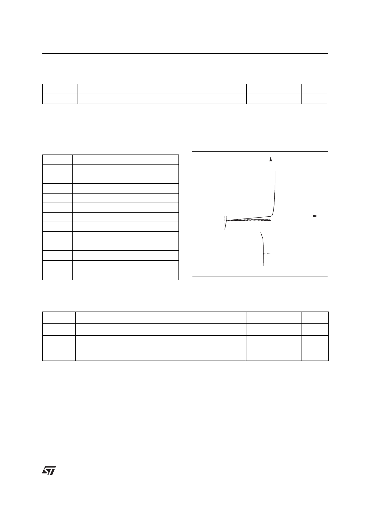
Symbol Test conditions Max Unit
V
F
V
FP
(note 1)
Note 1
: see test circuit for VFP; RP is the protection resistor located on the line card.
Square pulse : tp = 500µs IF = 5A
10/700µs
1.2/50µs
2/10µs
1.5kV
1.5kV
2.5kV
RP = 10Ω
R
= 10Ω
P
R
= 62Ω
P
2V
5
V
7
12
3/9
 Loading...