

SGS Thomson Microelectronics LCP02-150B1 Datasheet
®
LCP02-150B1
A.S.D.™
FEATURES
Protection IC recommended for ringing SLICs.
■
Wide firing voltage range: from -110V to +95V.
■
Low gate triggering current: IG= 5mA max.
■
Peak pulse current: IPP= 30A (10/1000µs) .
■
Holding current: IH= 150mA min.
■
UL497B approved (file E136224)
■
MAIN APPLICATIONS
Dual battery supply voltage SLICs
■
- negative battery supply configuration
-negative & positivebattery supply configuration
■ Central Office (CO)
■ Private Branch Exchange (PBX)
Digital Loop Carrier (DLC)
■
■ AsymmetricalDigital Subscriber Line(ADSL G.Lite)
■ Fiber in the Loop (FITL)
■ Wireless Local Loop (WLL)
■
Hybrid Fiber Coax (HFC)
■
ISDN Terminal Adapter
■
Cable modem
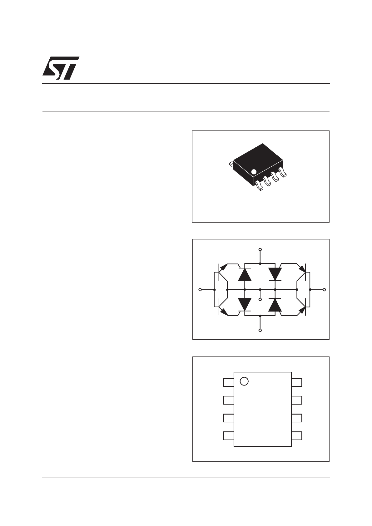
PROTECTION IC
FOR RINGING SLICS
SO-8 WIDE
FUNCTIONAL DIAGRAM
TIP
Gn
GND
Gp
DESCRIPTION
The LCP02-150B1 has been developed to protect
SLICsoperatingonboth negativeand positivebattery supplies, as well as on high voltage SLICs. It
providescrowbar modeprotection for bothTIP and
RINGlines. Thesurge suppression isassumed for
each wire by two thyristor structures, one dedicated to positive surges the second one for negative surges. Both positive and negative threshold
levels are programmable by two gates (Gn and
Gp). The use of transistors decreases the battery
currents during surge suppression.
The LCP02-150B1 has high Bellcore Core, ITU-T
and FCC Part 68 lightning surge ratings, ensuring
rugged performance in the field. In addition, it is
also specified to assist a designer to comply with
UL1950, IEC950 and CSA C22.2. It is UL 497B
approved (file E136224), and has UL94-V0resin
approved
TM: ASD is trademarks of STMicroelectronics.
September 2000 - Ed: 4A
RING
PIN-OUT CONFIGURATION
TIP
G
n
G
P
RING
NC
GND
GND
NC
1/8
LCP02-150B1
COMPLIES WITH FOLLOWING STANDARDS
ITU-T K20
ITU-T K21
VDE0433
VDE0878
IEC61000-4-5
FCC Part 68
lightning surge type A
FCC Part 68
lightning surge type B
BELLCORE
GR-1089-CORE
First level
BELLCORE
GR-1089-CORE
Second level
BELLCORE
GR-1089-CORE
Intrabuilding
Peak surge
voltage
(V)
4000
1000
4000
1500
Voltage
waveform
(µs)
10/700
10/700
10/700
10/700
Required
peak current
(A)
100
25
100
37.5
Current
waveform
(µs)
5/310
5/310
5/310
5/310
Minimum serial
resistor to meet
2000 10/700 50 5/310 5
2000 1.2/50 50 1/20 0
level 3
level 4
1500
800
10/700
1.2/50
10/160
10/560
50
100
200
100
5/310
8/20
10/160
10/560
1000 9/720 25 5/320 0
2500
1000
2/10
10/1000
500
100
2/10
10/1000
5000 2/10 500 2/10 40
800
1500
2/10
2/10
100
100
2/10
2/10
standard (
50
0
50
0
5
25
20
15
20
25
0
0
)
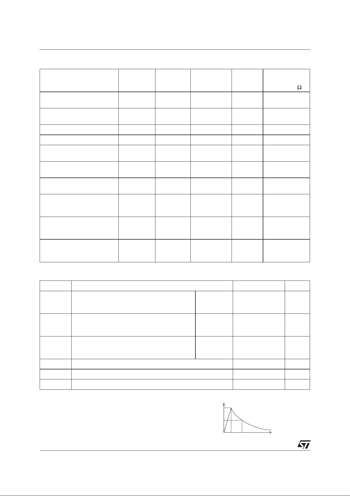
ABSOLUTE MAXIMUM RATINGS (T
amb
=25°C)
Symbol Parameter Value Unit
I
I
TSM
PP
Peak pulse current
Non repetitive surge peak on-state current
(F = 50Hz)
V
max
GN
max
V
GP
∆ V
bat
T
op
T
stg
T
L
Note 1: Within the Top range, the LCP02-150B1 keeps on operating.
The impacts of the ambient temperature are given by derating
curves.
Maximum negative battery voltage range
Maximum positive battery voltage range
Total battery supply voltage
max
Operating temperature range (see note 1)
Storage temperature range
Lead solder temperature (10s duration)
10/1000µs
5/310µs
1/20µs
= 0.2 s
t
p
=1s
t
p
=15min
t
p
30
45
65
5.5
4.2
1.5
See fig.1 -110to 0
0to+95
190
-20 to +85 °C
-55to+150 °C
260 °C
%I
PP
100
50
0
t
t
p
r
t
A
A
V
2/8
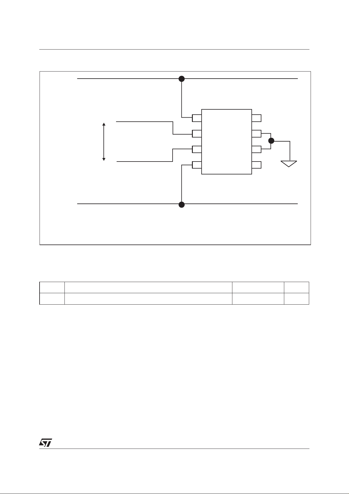
Fig. 1: Test circuit
TIP
LCP02-150B1
Gn from -110V to +0V
∆≤Vbat 190V
RING
Gn connected to negative supply voltage
Gp connected to positive supply voltage
ba GpGn
V t: differential voltage betweenV and V∆
THERMAL RESISTANCE
Gp from +0V to +95V
1
TIP
n
G
P
G
RING
NC
GND
GND
NC
Symbol Parameter Value Unit
R
th (j-a)
Junction to ambient
150 °C/W
3/8
 Loading...